Note: Descriptions are shown in the official language in which they were submitted.
CA 02501108 2005-04-O1
WO 2004/032407 PCT/US2003/030973
[0001] OPTIMUM INTERPOLATOR METHOD AND APPARATUS
FOR DIGITAL TIMING ADJUSTMENT
[0002] ~ FIELD OF INVENTION
[00M] This invention generally relates to digital timing synchronizers, and
more particularly to an efficient implementation of an interpolator to be used
in
digital timing synchronizers.
[0004] BACKGROUND
[0005] Hereafter, a wireless transmit/receive unit (WTRU) includes, but is
not limited to, a user equipment, mobile station fixed or mobile subscriber
unit,
pager, or any other type of device capable of operating in a wireless
environment.
When referred to hereafter, a base station includes, but is not limited to, a
base
station, Node B, site controller, access point or other interfacing device in
a
wireless environment.
[0006] In a wireless frequency division duplex (FDD) or time division
duplex (TDD) telecommunication system, timing synchronization between
transmitted and received signals of a base station and a WTRU is imperative
for
proper two way communication. Also, Doppler effect may contribute to the
frequency difference if the mobile receiver is in motion. To counteract the
timing
difference between the base station local oscillator and the WTRU local
oscillator,
a simple adjustment to the WTRU receiver local oscillator can correct the
error
by applying an advance or delay to the sampling rate accordingly, if there is
no
multipath processing in the receiver. However, due to multipath signal
effects,
conventional receivers of wireless communication systems employ means for
detection of the multipath signals and means for reconstructing the
transmitted
signal, such as the RAKE type receivers.
[0007] The timing for each path is estimated in two stages. First, a channel
estimator is used to find the approximate locations of each path in time for a
multi-path communication channel. Second, for each path, a dedicated code
tracker used in correlation to each R,AKF finger finds the accurate location
of the
-1-
CA 02501108 2005-04-O1
WO 2004/032407 PCT/US2003/030973
path in time and tracks it continuously thereafter. Since each path has a
unique
time location, controlling the code timing through the local oscillator alone
does
not correct the timing error in a multipath channel environment.
[0008] To address the multipath problem, code trackers may use
interpolators to perform digital timing synchronization instead of controlling
the
local oscillator. For the efficient implementation of an interpolator, a
finite
impulse response (FIR) interpolator may be used. There are different known
approaches for FIR interpolators. The simplest approach is to use a truncated
sans function as an FIR interpolator. Another option is to use a polynomial
interpolator. Also, a minimum mean square error (MMSE) interpolator can be
used. Among all of these algorithms, an MMSE interpolator provides the
minimum error compared to the infinite length ideal interpolator. It is to be
noted that without an efficient interpolator control unit that ensures that
the
interpolator is centralized with respect to the main lobe of the sync function
(i.e.,
centralized with respect to the interpolating function), the interpolator
might
result in a higher number of FIR coefficients than may be necessary for a
given
accuracy. The drawback to excessive coefficients is that the number of
interpolation computations becomes cumbersome, and at some point, a limiting
factor for the implementation. This is especially compounded as the number of
trackers employed increases in order to more effectively contend with
multipath
effects. Thus, a tradeoff exists between extending the number of RAKE finger
trackers versus the amount of time diversity gain obtained from a multi-path
channel.
[0009] SUMMARY
[0010] A digital timing synchronizer of a receiver is provided for timing
synchronization to a transmitter in a wireless communication system, wherein
the received signal has a timing error with respect to a reference code. A
channel
estimator estimates an initial code phase of the received signal. A code
generator
generates a timing reference code that is adjustable by integer increments. An
interpolation feedback circuit is configured for interpolation and correction
of the
CA 02501108 2005-04-O1
WO 2004/032407 PCT/US2003/030973
timing error, whereby the interpolation is achieved through an integer code
shift,
plus a quantized fractional delay estimate selected from a look-up table of
quantized values of fractional delay estimates associated with predetermined
interpolator coefficients, from which a time corrected version of the received
signal is produced.
[0011] Within the interpolation feedback circuit, an interpolator
normalized to a sampling rate is configured to shift the received signal in
time by
a fractional delay or advancement. A timing error estimator determines a
timing
error estimate based on the timing difference between an output signal of the
interpolation feedback circuit and the timing reference code of the code
generator.
An interpolator controller, responsive to the timing error estimate, produces
and
sends an integer code shift signal to the code generator in a direction
opposite of
the timing error estimate, and produces a fractional delay estimate, whereby
the
interpolation is controlled by maintaining fractional delay estimate within a
predetermined range. A quantizer, having the look-up table with stored
predetermined interpolator coefficients associated with quantized fractional
delay estimate values, selects a quantized fractional delay estimate that is
closest in value to the fractional delay estimate. The interpolator processes
the
coefficients associated with the quantized fractional delay estimate.
[0012] BRIEF DESCRIPTION OF THE DRAWINGS)
[0013] A more detailed understanding of the invention may be had from the
following description of a preferred embodiment, given by way of example and
to
be understood in conjunction with the accompanying drawings in which:
[0014] FIG. 1 shows a block diagram of a code tracker with optimized
interpolation;
[0015] FIG. 2 shows a block diagram of a loop filter; and
[0016] FIGS. 3A, 3B show timing diagrams of code shifting of the code
tracker.
-3-
CA 02501108 2005-04-O1
WO 2004/032407 PCT/US2003/030973
[0017] DETAILED DESCRIPTION OF THE PREFERRED EMBODIMENTS)
[0018] Although the embodiments are described in conjunction with a third
generation partnership program (3GPP) wideband code division multiple access
(W-CDMA) system utilizing the time division duplex mode, the embodiments are
applicable to any hybrid code division multiple access (CDMA)/time division
multiple access (TDMA) communication system. Additionally, the embodiments
are applicable to CDMA systems, in general, such as the proposed frequency
division duplex (FDD) mode of 3GPP W-CDMA.
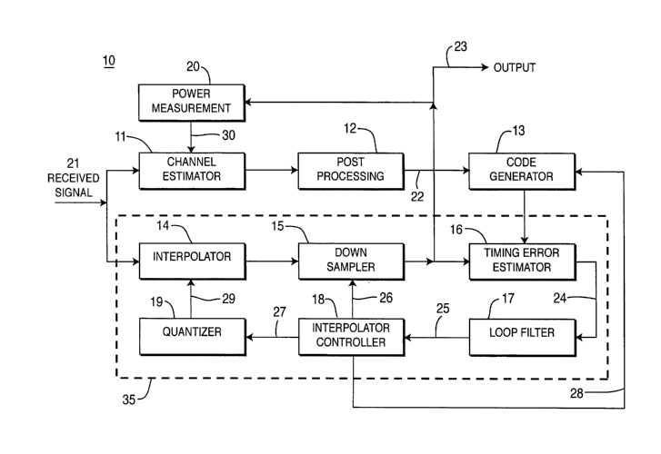
[0019] FIG. 1 shows a block diagram of the preferred embodiment of a code
tracker 10, comprising channel estimator 11, post processing unit 12, code
generator 13, interpolator 14, down-sampler 15, timing error estimator 16,
loop
filter 17, interpolator control 18, quantizer 19, and power measurement 20. A
received signal 21 becomes an input signal to both the channel estimator 11
and
the interpolator 14. Code tracker 10 performs digital timing synchronization
of a
receiver to a corresponding wireless transmitter. In a 3GPP-like system for
example, code tracker 10 is within a mobile WTRU receiver for digital timing
synchronization with a base station transmitter.
[0020] Channel estimator 11 coarsely estimates the initial code phase of
input signal 21, i.e., the code locations in time. One method for estimating
the
channel estimate includes, but is not limited to, using a sliding window
correlators. The sample period of the channel estimator 11 should be less than
or
equal to 2T~, where T~ is the duration of one chip period. For example; if an
early-
late gate synchronizer is used for timing error estimator 16, then the initial
timing error estimate should be confined to a range -T~ to T~. Otherwise, the
timing error may be out of range and the algorithm may fail to operate.
However,
this invention is not limited to early-late gate synchronizer and any other
timing
error estimator 16 may be used. In the latter case, a different sample period
for
the channel estimator can be used. By using a channel estimator 11 with a
sample period that is less than 2T~, the initial error in the path location is
limited
to the range -T~ to T~.
-4-
CA 02501108 2005-04-O1
WO 2004/032407 PCT/US2003/030973
[0021] Post-processing unit 12 estimates the signal and noise power
against a noise threshold. After the post-processing is completed, all the
paths
that have the power level above the noise threshold are identified. Location
of
these strong paths in time is called the initial code phase 22. Either the
strongest
one of these paths may be used alone, or a set of paths above a certain
threshold
may be used as in a RAKE-like receiver structure. A RAKE-like receiver is very
useful in a multipath channel environment since it makes efficient usage of
the
time diversity of the channel.
[0022] In the case having a selected strongest path, there is only one code
tracker 10, including one interpolator 14 and one interpolator control 18. For
a
RAKE-like receiver, there should be one code tracker 10 dedicated to each path
used. In that case, however, the channel estimator 11 and the post-processing
unit 12 will be common to all the code trackers used. By applying the initial
code
phase 22 for a single path from the post-processing unit 12 to the code
generator
13, the timing synchronization begins.
[0023] For each code tracker 10 of a RAKE-like receiver, a code generator
13 produces a reference code for the basic timing, functioning as a clock.
Initial
code phase 22 adjusts the initial timing offset of the code generator 13 in
multiples of chips by simply advancing or delaying in time the reference code
being generated. After the initial correction is completed, the code generator
13 is
only controlled by the code shift command 28 coming from the interpolator
control 18. The initial code phase 22 is only being applied under two
circumstances: the first time the receiver is activated, and anytime the
signal
power drops below a noise threshold. Code shift 28 is a shift command of one
chip
generated by the interpolator controller 18 in either an advance or delay
direction. After the initial correction is completed, the worst-case timing
error
estimate is confined to a period range of -T~ to T~.
[0024] The interpolation feedback loop 35 of code tracker 10, comprising
interpolator 14, down-sampler 15, timing error estimator 16, loop filter 17,
interpolator controller 18, and quantizer 19, will now be explained in detail.
Interpolation feedback loop 35 drives the timing error estimate signal 24 to a
CA 02501108 2005-04-O1
WO 2004/032407 PCT/US2003/030973
value close to zero, and drives the delay estimate 25 towards the actual delay
duration.
[0025] Interpolator 14 shifts the received signal in time mathematically
with an amount equal to the quantized fractional delay estimate 29, received
from quantizer 19. The output signal from an ideal interpolator is represented
by
Equation 1:
y(ra) = x(ya + a) = ~ x(Ta - nt)Sinc(m +a) , Equation 1
m=-m
where n is an integer time index, x(n) is the over-sampled received signal 21,
&
represents the quantized fractional delay estimate 29, and the Sinc function
is
defined as:
Sinc (x) = Sin(~x) . Equation 2
~r..e
For the initial iteration through interpolation feedback loop 35, quantized
fractional delay estimate 29 is reset to zero, which results in the received
signal
passing through the interpolator 14 unmodified. Regarding operation of
interpolator 14 and formulation the quantized fractional delay estimate 29
(i.e.,
value iz ), a description in further detail will follow in reference to the
second and
beyond iterations of interpolation feedback loop 35.
[0026] Down-sampler 15 reduces the over-sampling rate of the received
signal 21 by an over-sampling factor of L after it has been processed by
interpolator 14. Code tracker 10 with interpolator 14 can be applied to a
receiver
that operates at a sampling rate of any integer value of L greater than or
equal to
one. The optimum range for sampling rate to which code tracker 10 can perform
timing adjustment is 1 <_ L <_ 8. The case L = 1 corresponds to no over-
sampling.
If, on the other hand, the sampling rate correlates to an integer L >_ 8, the
timing
error reduces to a value on the order of 1/16T~ , whereby the contribution of
interpolator unit 14 is significantly reduced and a simple sample shift
through
the down-sampler 15 begins to be sufficient on its own. However, as high over-
sampling rates such as L >_ 8 results in extra power consumption of receiver
-6-
CA 02501108 2005-04-O1
WO 2004/032407 PCT/US2003/030973
resources, it is advantageous to operate at lower sampling rates and perform
code
tracking with code tracker 10 according to FIG. 1.
[0027] Down-sampler 15 converts the sampling rate to the chip rate, such
that at the output of down-sampler 15, the sampling rate period TS equals the
chip rate period T~. Therefore, the output of the down-sampler 15 can be
represented by z(n> as follows:
z(ra) = y(L ~ ~ + k) Equation 3
where h is an integer representing the base point 26 of the down-sampler 15.
For
example, for an over-sampled signal with sampling rate factor L=4, the period
of
the sampling rate prior to down-sampler 15 is TS = T~ lL = T~ l4, while after
the
down-sampling, it is TS = T~ . Initially, the base point 26 is reset to zero.
The
derivation of value h will be explained later in reference to Equations 6a,
6b.
[0028] The output of down-sampler 15 is the time corrected output signal
23 to be further processed by the WTRU receiver. Power measurement unit 20
processes the output 23 and sends the power measurements of the signal to
channel estimator 11 as an input for locating the approximate locations of
each
path in time for the multipath channel. For timing refinement, the output 23
of
down-sampler 15 also continues through interpolation feedback loop 35 of code
tracker 10, to timing error estimator 16, where the timing error of the input
signal is measured and sent as timing error estimate 24. Timing error
estimator
16 can operate according to a variety of known timing error estimation
algorithms. The preferred embodiment employs an early-late gate synchronizer.
[0029] Next, a loop filter 17 receives timing error estimate 24 to produce a
delay estimate 25. The selection of the type of loop filter 17 depends on the
channel conditions. However, the invention is not limited to the particular
loop
filter being used. Preferably, loop filter 17 is a first or second order
filter. As an
example, a known proportional integrator (PI) filter is used as loop filter
17.
Alternatively, a first order auto regressive (AR) filter is be used as loop
filter 17.
[0030] FIG. 2 shows a preferable configuration for loop filter 17, comprising
a second order PI filter 50, accumulator 56, and inverted multiplier 57. PI
filter
_7_
CA 02501108 2005-04-O1
WO 2004/032407 PCT/US2003/030973
50 comprises integrator 51, which includes multiplier 52 and accumulator 53,
multiplier 54 and adder 55. Multipliers 52 and 54 apply constants a and b,
respectively to the timing error estimate 24 input, which is split at the
input of
PI filter 50. The timing error estimate 24 input is integrated by integrator
51,
while multiplied by constant b in parallel with the integrator 51. The
parallel
outputs are summed by adder 55 to produce the PI filter output. Next, the PI
filter output is accumulated by accumulator 56 and processed by multiplier 57
with a constant -c. The sign reversal of constant c in multiplier 57 results
in the
timing correction in the opposite direction to compensate for the timing error
estimate 24 in the signal, useful for a negative feedback system such as shown
in
FIG. 1. Depending on the order of the loop filter 17, the code tracker 10 can
include a first, second or even higher order feedback loop. The output of
multiplier 57 is delay estimate 25.
[0031] The output delay estimate 25 of loop filter 17 is represented by Ta as
follows:
Td = - s(Te ) , Equation 4
where T~ is the timing error estimate 24 from the timing error estimator 16,
and
s(.) is a linear operator. The delay estimate 25 is passed to the interpolator
control 18 for further processing.
[0032] Interpolator controller 18 serves two main functions: regulating
delay estimate 25 range and minimizing interpolator coefficients. First, with
respect to keeping the delay estimate 25 within the operating range for the
rate
of the code tracker 10, the operating range depends on the particular
selection of
the timing error estimator 16. For example, for an early-late gate
synchronizer
type timing error estimator 16, the operating range sampling period is limited
to
-T~ to T~. There are two ways of limiting the signal timing deviation to the
working range of the timing error estimator 16. First, this can be achieved by
shifting the base point 26 of the down-sampler 15 in time proportional to the
delay estimate 25. However, this corresponds to changing the beginning of the
frame for the whole receiver. It is only realizable if there is only one
direct
_g_
CA 02501108 2005-04-O1
WO 2004/032407 PCT/US2003/030973
transmission path to the receiver. However, in a multi-path environment, it is
preferable to shift the code generator 13, of the code tracker 10 dedicated to
the
path of concern, in the opposite direction of the delay estimate 25.
[0033] Independent of the timing error estimator 16 implementation, the
timing error estimate 24 of the received signal 21 is measured with respect to
the
reference code in the receiver, which is produced by code generator 13.
Interpolator control 18 monitors the delay estimate 25 and whenever it is
outside
of a certain range, it shifts the code generator 13 in the opposite direction.
Since
the code generator 13 is working at a chip rate with period T~, the minimum
amount of shift is equal to the chip duration, i.e., T~. Therefore, it is
preferable to
perform a code shift 28 whenever delay estimate 25 becomes Td > T~ l 2 or
Td < -T~ l 2 .
[0034] In actual communication system implementations, the relative
delay of the path between the base station and the mobile WTRU receiver may
change over time. Mainly, this may occur for the following reasons. First, the
motion of a mobile WTRU receiver can result in a change of the delay estimate
25
in time. For a mobile WTRU receiver moving with a constant speed, there is a
first order change in the timing error. A second reason is the local
oscillator
frequency differences between a base station and a mobile WTRU receiver. This
also results in a first order change in the delay estimate 25. Both of these
effects
are cumulative. However, the timing error changes are not limited to first
order
changes. For code tracker 10 having N order changes, interpolator controller
18 is
able to follow N-1 order changes if necessary, and performs code shifts
whenever
necessary.
[0035] The code shift decisions by code tracker 10 are robust, not
withstanding low signal-to-noise ratio (SNR) and fading channel conditions. To
eliminate the oscillating code shift operations due to noise and interference,
simple hysteresis logic is employed. Timing diagrams of the delay estimate 25
change with respect to oscillator drift and a constant speed mobile WTRU
motion
are shown in FIGS. 3A and 3B. The time shifts result in saw-tooth waveform
-9-
CA 02501108 2005-04-O1
WO 2004/032407 PCT/US2003/030973
structure due to periodic time shifts for a linearly changing time delay. As
shown
in FIG. 3A, delay estimate 25 is linearly increasing. The peak transitions
occur at
a code shift 28, where at peak T~12 + ~ , code shift 28 is implemented in a
negative
direction to compensate for the increasing delay estimate 25. Conversely, in
FIG.
3B, a linearly decreasing delay estimate 25 is compensated by a positive code
shift 28. Although a linear change of time delay 25 is depicted in FIGS. 3A
and
3B, it should be noted that code tracker 10 is not restricted to linear
changes in
delay estimate 25, but will work for any kind of change in the delay estimate
25
updates. The code shift 28 takes place in both directions, either with delay
or
advance as before explained. As shown in FIGS. 3A and 3B, an arbitrary small
value of ~ (e.g., O.OST~ ) is used to prevent oscillatory behavior around the
code
shift 25 points.
[0036] After the code shift 28 occurs, the new delay estimate value 25 that
is used by the interpolator controller 18 is found as follows:
Td =Td -T~ sgn[Td], Equation 5a
where sgn [.] indicates the direction of code shift 28 (i.e., positive,
negative, or
none) and is defined as:
l, Td >_T~12+0
sgn[Td ] = 0,-T~ / 2 - D < Td < T~ l 2 + 0 Equation 5b
-1, Td -<-T~12-~.
[0037] Regarding the second function of interpolator controller 18 to
minimize coefficients, the actual interpolation with finite size is optimized
to
achieve minimum error. Recall that the ideal interpolator in Equation 1 has
infinite number of coefficients and as such is not realizable in an
implementation.
The optimum interpolator coefficients for a finite size interpolator are
obtained
through an optimization algorithm, such as MMSE, to minimize the
approximation error. This is described in the following paragraphs in detail.
However, the approximation error due to a finite size interpolator can be
further
-10-
CA 02501108 2005-04-O1
WO 2004/032407 PCT/US2003/030973
reduced, by minimizing the fractional delay estimate 27 as much as possible.
Interpolator controller 18 is therefore configured to achieve this. The delay
estimate 25 after code shift processing can be written as
T~ = k ~ TS + a ~ TS , Equation 6a
where h is defined as follows:
k = T Equation 6b
S
The operation Lx J represents the largest integer in x. The value of k
corresponds
to the number of over-sampled sample durations that exist in Td . Therefore, a
delay or advance of k ~ TS corresponds to a simple shift of the over-sampled
input
signal by an amount equal to k samples. This shift is easily achieved by
shifting
the base point 26 of the down-sampler by an integer k as shown in Equation 3.
After the base point 26 shift, the remaining time shift left is equal to
Td =Td -k~TS =a~TS. Equation 7
Since the interpolator 14 is normalized to the sampling rate of TS , the value
that
goes to interpolator 14 is the fractional delay estimate 27 after it is
quantized
(i.e., a ). Also, it is important to note that after decomposing delay
estimate 25
(i.e., value Td in Equation 6a and value h in Equation 6b), fractional delay
estimate 27 is limited to the range -1 < a < 1. This limiting of the range
keeps
fractional delay estimate 27 minimal and achieves the desired decreased
interpolation error.
[0038] To illustrate the operation of the interpolator controller 18, the
following example is presented. Assume that the filtered timing error estimate
25
is Td = 0.64T~ and the over-sampling rate is L=4. Therefore, the sampling rate
is
TS = T~ l L = T~ l4 . According to Equations 5a and 5b, code shift 28 is
required,
and so the code shifted delay estimate 25 is Td = 0.64T~ -T~ _ -0.36T~ . From
Equation 6b, base point 26 is h = -1 and from Equation 6a, the fractional
delay
estimate 27 is a = -0.44 .
-11-
CA 02501108 2005-04-O1
WO 2004/032407 PCT/US2003/030973
[0039] Quantizer 19 is the last remaining stage of interpolation feedback
loop 35. The fractional delay estimate 27 is quantized (i.e., discretized) by
the
quantizer 19 before being used by the interpolator. Quantizer 19 is useful for
limiting computation of the interpolator coefficients to avoid the computation
each time the delay estimate 25 is updated. Quantizer 19 comprises a look-up
table for storing pre-calculated interpolator coefficients that correlate to a
set of
available quantized fractional delay estimate values. This look-up table
decreases
the computational complexity of the interpolation and also increases the
processing speed. Quantizer 19 determines a number of levels for quantizing
the
fractional delay estimate based on the required timing accuracy and the over-
sampling rate L. The required timing accuracy for timing adjustment is T~ l Q
,
where Q is a positive integer. It follows that the quantization step size
needed is
2T~ l Q . For the over-sampling rate of L, this corresponds to Q l L
quantization
levels for the range -1 < cz < 1. For example, for Q=32 and L = 4, the
required
timing accuracy for timing adjustment is T~ / 16 , and the quantizer 19 has Q
l L =
8 levels. Then if fractional delay estimate 27 is a = -0.44 according to the
above
example, the quantized delay would be determined from selecting the nearest
equivalent value from the lookup table in quantizer 19. Since this is a level
8
quantizer, the available values are from the following set of quantized
fractional
delay estimates: [-1, -0.75, -0.5, -0.25, 0.25, 0.5, 0.75, 1] (value 0 is not
used as
it results in no interpolation at all). Since -0.44 is closest to -0.5, the
selected
quantized fractional delay estimate 29 is then a = -0.5, which is passed to
the
interpolator 14.
[0040] Following the initial iteration of the interpolation feedback loop 35,
the delay estimation and interpolation operation is continuously repeated to
track the changes in the timing error.
[0041] Returning to interpolator 14, the finite interpolation of Equation 1
will now be described, including interpolator 14 processing a quantized
fractional
delay estimate 29 where a ~ 0, unlike when interpolator 14 initially processes
the received signal 21. As seen from Equation 1, the ideal interpolation is an
-12-
CA 02501108 2005-04-O1
WO 2004/032407 PCT/US2003/030973
infinite length summation. For efficient interpolator implementation, a finite
summation of Equation 1 must be performed. Equation 8a below shows this finite
representation of output x as follows:
Mz
x (tt + a) _ ~ x(n - tn)ha (tt) Equation 8a
m=-M~
where ha (n) represents interpolator coefficients, derived as follows:
hs (tt) = Sitzc(m + a) Equation 8b
The frequency response of an ideal interpolator, which is an infinite length
filter,
is as follows:
TSe jeoaTS ~ ~~Z~I < 1 /(2TS )
S(c~, aT,~ ) = Equation 9
0, othet~wise
An output signal error E(a) is defined as the difference between the ideal
interpolator output and the finite representation of the interpolator as
follows:
E(a) = x (tt + a) - x(zz + a) Equation 10
[0042] Coefficients ha (tt) of an optimum FIR interpolator are determined
by minimizing Equation 11, below, for all possible & values for the quantized
fractional delay estimate 29. The optimization method used is a minimum mean
square error (MMSE) approach. Since the bandwidth F =c~/2n of interest is
smaller than 1/(2TS), applying Parseval's relation to Equation 10 yields:
F 2
EZ (&) = f e'°'aTS - ~ ha (rt)e-'~'"TS d~ Equation 11
-F n=-M~
Equation 11 is representative of an MMSE version of an FIR filter, which is
the
preferable type of interpolator for interpolator 14. Equation 11 has several
different solutions. As an example, the Fletcher-Powell method can be used to
solve Equation 11. It should be noted that the embodiments of the invention
are
not limited to any particular solution of Equation 11. The minimum error E(a)
is
achieved if (Ml = M) and (Ms = M-1) are selected for a total number of 2M
-13-
CA 02501108 2005-04-O1
WO 2004/032407 PCT/US2003/030973
coefficients. With coefficients found from Equation 12, optimum MMSE FIR
interpolator 14 can be represented by the following equation:
M-1
x (n + ce) _ ~ x(n - m)ha (fn) Equation 12
m=-M
As one skilled in the art knows, the interpolator coefficients are symmetrical
around a = 0.5 , which can be written as
h~t_a~ (nZ) = ha (-na -1) Equation 13
As it is not feasible to solve for Equation 11 in real-time, Equation l1 is
solved
for all the possible iz values in advance, and the predetermined coefficients
are
stored in the look-up table of quantizer 19. This results in a look-up table
of real
number entries of size M ~ ((Q l L) - 2) , where Q l L is the number of
quantizer
levels. However, as a = 0 results in no interpolation at all, it is excluded
from the
quantizer 19 look-up table. By using the symmetry property of Equation 13, the
size of the look-up table can be reduced by half to M ~ ((Q l L) - 2) l 2 real
numbers.
Alternatively, depending on the implemented interpolator structure, such as a
polynomial interpolator, a look-up table may be omitted and replaced by real
time computation.
[0043] In implementation, there are 2M number of coefficients ha (n) for
M >-1, depending on the interpolation error that can be afforded. For example,
a
code tracker design for a 3GPP-like FDD compatible mobile WTRU receiver,
including an early-late gate synchronizer, two times over-sampling (L = 2),
and a
second-order loop filter including a PI filter cascaded with an accumulator as
shown in FIG. 2, results in M = 2 or total of four coefficients per quantizer
level.
For a required accuracy of T~ / 16 , (i.e., Q = 16), the number of quantizer
levels
used is eight.
[0044] By optimizing the interpolation in accordance with the present
invention, favorable results are achieved in reducing the timing error
efficiently
despite using a limited number of coefficients. Although the invention has
been
described in reference to multi-path fading channels and R,AI~E-like
receivers, it
should not be construed as limited to these applications. Alternative
-14-
CA 02501108 2005-04-O1
WO 2004/032407 PCT/US2003/030973
embodiments of code tracker 10 include, but are not limited to, having an
interpolator among the following types: polynomial FIR interpolator, linear
interpolator, and Lagrange interpolation.
-15-