Note: Descriptions are shown in the official language in which they were submitted.
CA 02501267 2005-04-04
WO 2004/031743 PCT/GB2002/004545
1
A WAVEGUIDE STRUCTURE
The present invention relates to waveguide structures and is particularly,
although not
exclusively, directed to waveguide structures suitable for use as optical
biosensors.
The recent increase in the prevalence of antibiotic-resistant bacteria and the
escalated
risk of biological warfare or terrorism have emphasised the need for a rapid
and cost
effective determination of the presence of pathogens in both the civilian. and
military
environment. Optical sensors provide a superior method for the detection of
pathogens in that they allow real-time monitoring of an environment according
to
changes in an optical property associated with a biological sample.
Optical sensors are commonly based on layered optical waveguide structures in
which
an evanescent wave associated with an optical mode existing in the structure
extends
into a sensing layer comprising the biological sample. A change in the
refractive
index, for example, of the sample by interaction or binding to the pathogen
leads to a
change in an optical property of the mode, which can be readily detected.
Optical
waveguide structures have been used to detect pathogens such as bacteria,
viruses and
toxins in water.
One such optical evanescent sensor uses the phenomenon of surface plasmon
resonance (SPR). Here the sensor comprises a dielectric prism in which an
upper
surface is coated with a thin metal layer of gold or silver and a sensing
layer
comprising the biological sample is arranged on the metal layer. Light
incident the
upper surface of the dielectric prism at angles greater than the critical
angle for total
internal reflection is monitored by a detector. At a certain "resonant" angle
or angles,
CA 02501267 2005-04-04
WO 2004/031743 PCT/GB2002/004545
2
the incident light is coupled to oscillations of the electron cloud in the
metal layer and
is propagated at the interface of the prism and the metal layer. A drop in the
amount
of reflected light is detected at the detector. The surface optical mode
generates an
evanescent field that extends into the sensing layer and is sensitive to a
change in the
S refractive index of the biochemical sample. A pathogen binding to tie sample
is
detected at the detector by a change in the angle at which resonance is
excited.
The sensitivity of optical sensors based on surface plasmon resonance is in
general
restricted in that the range of angles at which the incident light will excite
resonance is
small. The problem is particularly acute for the detection of particles where
the
requirement for a relatively large change in the refractive index of the
biochemical
sample is compounded by poor extension of the evanescent field into the
sensing
layer. A further disadvantage of optical sensors based on surface plasmon
resona~ice
is that they require polarised light.
One approach to the problem of poor sensitivity, described in International
Patent
Application No. WO 99/44042, relies on optical sensors comprising "leaky"
waveguide structures. The basic "leaky" waveguide structure is similar to the
surface
plasmon resonance structure in that it comprises a sensing layer disposed upon
a thin
metal layer coating a transparent substrate. However, the refractive indices
of the
layers are chosen so that light incident the upper surface of the substrate is
not wholly
internally reflected but coupled through the metal layer into (and out of) an
optical
mode propagating in the sensing layer.
CA 02501267 2005-04-04
WO 2004/031743 PCT/GB2002/004545
3
WO 99/44042 describes a number of other leaky waveguide structures. One
structure
(a resonant optical waveguide, ROW) comprises a sensing layer provided on a
layer
of high refractive index, which is disposed upon a spacer layer separating it
from the
substrate. In this structure, which is similar to a resonant mirror structure,
light
S incident the upper surface of the substrate is coupled via an evanescent
field in the
spacer layer into an optical mode supported in the layer of high refractive
index. The
optical mode has itself an associated evanescent field, which extends into the
sensing
layer. A further structure (an anti-resonant reflecting optical waveguide,
ARROW)
comprises an additional spacer layer between the layer of high refractive
index and
the sensing layer. The refractive indices and thicknesses of each layer are
chosen so
as to maximise the reflection of propagated light in the leaky waveguide mode
by
constructive interference and to minimise its loss by destructive
interference.
It will be understood that because the leaky waveguide structures of WO
99/44042
support an optical mode centred on the bulk of the sensing layer (a "bulk"
optical
mode) they offer greater sensitivity than waveguides based supporting surface
modes.
A further advantage of the waveguide structures of WO 99/44042 is that they
can
provide an easily observed peak, rather than a dip, in the intensity of
reflected light.
for a large change in the refractive index of the sample.
Improved sensitivity of detection of particulate pathogens is obtainable by
examination of light scattered or emitted by interaction of particles with an
optical
mode. International patent application No. WO 01/42768 describes the use of
surface
plasmon resonance to detect particles by scattering or emission of light. The
sensitivity of the technique is limited by the fact that the extension of the
evanescent
CA 02501267 2005-04-04
WO 2004/031743 PCT/GB2002/004545
4
field in the sensing layer is low (about 100 to 250 nm) and therefore overlaps
only a
small proportion of the bulk of particles such as bacteria (about 1 ~.m in
diameter).
Further, because the intensity of scattered or emitted light is proportional
to the
intensity of the evanescent field, which diminishes exponentially in the
sensing layer,
poor extension of the field means that particles further from the interface of
the
sensing layer with the metal may not be detected.
The leaky waveguide sensors of WO 99/44042 are also limited in their ability
to
detect pathogens by scattering of light. In particular, the pore si;~es must
be
constrained in order to avoid them scattering light and thus can only admit/
particles of
diameters less than 20 nm. Consequently larger particles such as bacteria and
some
viruses cannot be detected using this method.
The present invention generally aims to overcome these problems by providing a
waveguide sensor in which an evanescent field penetrates a sensing layer to a
greater
extent and overlaps with at least a major proportion of the bulk of the
particle. The
present invention lies in the realisation that a leaky waveguide optical mode
supported
in a layer of low refractive index adjacent a sensing layer can increase the
depth of
penetration of an evanescent field in the sensing layer.
The present invention therefore provides a waveguide structure comprising a
sensing
layer of a medium disposed upon a second layer, said second layer being
disposed
upon a third layer of differing refractive index to the second layer, in which
the
structure is capable of supporting a bulk optical mode in the second layer,
the medium
is adapted to trap a target particle that results in a change in an optical
property of the
CA 02501267 2005-04-04
WO 2004/031743 PCT/GB2002/004545
S
sensing layer and the thickness and/or refractive index of the second layer is
selected
to control the depth of penetration of the optical mode into the sensing layer
and to
overlap at least a major portion of the particle.
It will be understood by those skilled in the art that the selection of
refractive index
and thickness of the second layer modulates the refractive index of the third
layer and
improves the optical mode and the depth of penetration of its evanescent field
in the
sensing layer. In general, the extent of penetration of the evanescent field
increases
with diminishing thickness and lower refractive index of the second layer.
Preferably,
the refractive index of the second layer is lower than the refractive index of
the third
layer.
The second layer also acts to increase the extent of propagation of the
evanescent field
in the sensing layer. The propagation of the mode in the sensing layer catv
reach a few
mm and is much higher than the few microns obtainable in surface plasmon
resonance
and resonant mirror waveguides. It will therefore be apparent that the second
layer
also increases the area of detection of a sensor based on the waveguide
structure.
In a preferred embodiment of the present invention, the second layer comprises
silica
in crystalline or sol gel form. However, the second layer may alternatively
comprise
other materials capable of supporting an optical mode such as agarose gel,
certain
fluorinated polymers or polyacrylates such as poly-2-
hydroxyethylmethylacrylate
(HydrogelTM).
CA 02501267 2005-04-04
WO 2004/031743 PCT/GB2002/004545
6
In a preferred embodiment of the present invention, the waveguide structure
comprises a fourth, absorbing layer, of high reflectivity, disposed between,
the second
layer and the third layer. The fourth layer may comprise a thin metal layer or
coating
provided on the upper surface of the third layer (in which case the structure
is
described as a "metal-clad" leaky waveguide, MCLW). Suitable motals include
aluminium, tantalum, zirconium, titanium or chromium. Alternatively the fourth
layer
may comprise a thin layer or coating of a crystalline dye material (in which
case the
structure is described as a "dye-clad" leaky waveguide, DCLW).
The inclusion of a fourth layer, is advantageous in that it furthers
propagation of the
optical mode in the second layer and increases the depth of penetration of the
evanescent wave in the sensing layer. The fourth layer therefore also improves
the
sensitivity of the waveguide structure. Further, when the waveguide mode is
not
excited, (i.e. it is in "off resonance" mode in which light is not coupled
into the
waveguide), almost all of the incident optical energy is deposited on the
layer in the
form of heat. Thus, at resonance, there is a sharp peak in the reflectivity of
the
MCLW or DCLW making detection of the resonant mode at a detector relatively
easy.
Suitable refractive indices n for the second layer, resulting in improved
detection of
bacteria of size 1 to 10 ,um, range from n 1.33 to 1.45 with suitable
thickT~esses for the
second layer ranging from 200 nm to 1000 nm. Preferably, the refractive index
and
thickness of the second layer is chosen so that the depth of penetration of
the
evanescent field 'overlaps the whole of the particle to be detected.
CA 02501267 2005-04-04
WO 2004/031743 PCT/GB2002/004545
7
In one embodiment of the present invention a second layer comprising silica
sol of
thickness 300 nm and a fourth layer comprising titanium of thickness ~.5 nm is
suitable to give a depth of penetration of the evanescent field of at least
1.5 ~m and
full overlap Bacillus globigii, (BG), spores (~ 1 ~,m).
S
The third, or "substrate" layer of the waveguide structure generally comprises
a light
transmitting material such as glass, Perspex~, quartz or a suitable polymer
and may
be associated with means for coupling light into and out of the second layer
of the
structure. Preferably, the substrate layer comprises an ordinary microscope
slide.
The waveguide structure of the present invention may be fabricated as a "chip"
which
can be adapted by the end user. The chip may be provided by coating a
conventional
microscope slide with a thin metal or dye layer, followed by spin coating or
vacuum
deposition of the silica layer. Whilst the thickness of the metal or dye layer
will be
1 S fixed at the time of manufacture, the present invention contemplates that
the thickness
of the silica layer or silica sol layer may be determined by subsequent
treatment of the
chip. In particular, the chip may be adapted. for the detection of one or more
particles
by, for example, etching the whole or a portion of the silica layer to give a
desired
thickness. Of course, in these circumstances the chip will be manufactured to
a
thickness of the silica or silica sol layer suitable for the detection of the
largest of
particles of potential interest. The final thickness of the silica or silica
sol layer is
determined by the end user and the disposition of the sensing layer on the
chip.
The sensing layer may comprise an antibody layer or coating, which is
chemically
deposited on the chip by standard reaction with chemical linking groups known
to the
CA 02501267 2005-04-04
WO 2004/031743 PCT/GB2002/004545
8
art. The antibody layer or coating may be continuous or partial and may, in
particular,
comprise a number of continuous or partial arrays of different antibodies each
speci~c
to a different particle to be detected. In one embodiment of the present
invention a
Bacillus globiggi antibody layer or coating is attached by sequential exposure
of the
chip to 3-aminopropyltriethoxysilane, glutaraldehyde and antibody.
It will be realised that the sensing layer of the present invention may
alternatively or
additionally comprise a fluid layer in contact with the upper surface of the
chip. The
fluid layer, which is semi-infinite, will contain the particles to be
detected. It will also
be realised that chemical or biochemical entities other than antibodies, which
are
specific to a particle to be detected, may be used in the sensing layer.
In one aspect of the present invention there is provided an optical sensor
comprising a
waveguide structure having a sensing layer of a medium disposed upon a second
layer, said second layer being disposed upon a third layer of_differing
refractive index
to the second layer, in which the structure is capable of supporting a bulk
optical
mode in the second layer, the medium is adapted to trap a target particle
resulting a
change in an optical property of the sensing layer and the thickness and/or
refractive
index of the second layer is selected to 'control the depth of penetration of
the optical
mode in the sensing layer and to overlap at least a major portion of the
target particle,
an optical source, means for coupling light from the optical source to the
optical mode
and means for detecting light scattered or emitted by the particle in, at or
adjacent the
sensing layer.
CA 02501267 2005-04-04
WO 2004/031743 PCT/GB2002/004545
9
The detecting means generally comprises a charge-coupled device (CCD) imager.
The detecting means may be associated with an imaging lens disposed between
the
sensing layer and the imager. Preferably, the imaging lens comprises two
achromatic
lenses and in conjunction with the CCD imager gives a resolution of about 4
,um per
pixel.
The detecting means is arranged above the upper surface of the chip to detect
scattered or emitted light from the particle. The emitted light may be due to
fluorescence although phosphorescence may also be used. Of course if emitted
light
is to be detected the particle must first be suitably labelled or otherwise be
a natural
emitter.
The wavelength of the incident light will be chosen not only to support
emission of
light by the particle but also to optimise the depth of penetration of the
evanescent
field in the sensing layer and provide a convenient angle of incidence of the
light at
the upper surface of the third layer.
The optical source generally comprises a source of coherent light. Where
fluorescence is to be detected the optical source may comprise an argon laser
providing light at 488 nm. A suitable filter removing scattered light is
placed in front
of the CCD imager. Where scattered light is to be detected, the filter may be
exchanged for one removing any emitted light or an optical source comprising a
semiconductor laser providing light at 635 nm wavelength may be used.
CA 02501267 2005-04-04
WO 2004/031743 PCT/GB2002/004545
The optical sensor may further include means for detecting changes in the
properties
of the optical mode by monitoring light coupled from the waveguide structure.
Although the peak of amplitude of reflected light at resonance is sharp, the
second
detector cannot detect individual particles in the way that the first detector
can, and is
5 provided solely for the purpose of maintaining the incident light at the
appropriate
resonant angle.
In a second aspect of the present invention there is provided a method of
detecting a
particle comprising the steps of i) exposing the optical sensor to the target
particle and
10 ii) detecting light scattered or emitted from the particle at the detecting
means.
In a further aspect of the present invention provides for use of a waveguide
structure
comprising a sensing layer of a medium disposed upon a second layer, said
second
layer being disposed upon a third layer of differing refractive index to the
second
layer, in which the structure is capable of supporting a bulk optical mode in
the
second layer, the medium is adapted to trap a target particle that results in
a change in
an optical property of the sensing layer and the thickness and/or refractive
index of
the second layer is selected to control the depth of penetration of the
optical mode into
the sensing layer and to overlap at least a major portion of the particle, in
a method of
detecting the particle.
It will be apparent to those skilled in the art that the invention provides a
technique
based on the collection of scattered or emitted light which improves on
surface
plasmon resonance and resonant mirror techniques by increasing the probability
and
extent of overlap of the evanescent field with the particle. Indeed the
invention makes
CA 02501267 2005-04-04
WO 2004/031743 PCT/GB2002/004545
11
possible detection of Bacillus globiggi at concentrations of 107 spores ml-1 -
an
improvement of two orders of magnitude compared to the prior art (typically
109
spores ml-1). Other advantages of the present invention include the fact that
unlike the
surface plasmon resonance technique there is no need to use plane polarised
light and
that much lower angles of incidence are used. Further, the waveguide
structures of
some embodiments of the present invention can be fabricated at room
temperature, are
cheaper to manufacture and can be disposable.
The present invention will now be described with reference to a number of
embodiments and the following drawings in which
Figure 1 is a diagram illustrating the generation of an evanescent field at
the
interface of media in which total internal reflection of light occurs;
Figure 2 is a schematic representation of a "leaky" waveguide structure;
Figure 3 is a cross sectional elevation view of a leaky waveguide structure
according to one embodiment of the present invention;
Figure 4 is a graph showing the optical mode supported in the waveguide
structure according to the embodiment of Figure 3;
Figure 5 is a graph showing the relative extent of the evanescent field in the
sensing layer for the embodiment of Figure 2 and for SPR and resonant mirror
waveguide structures;
Figure 6 is a schematic illustration of an optical sensor according to the
present invention;
Figure 7 is a graph illustrating the peak in reflectivity of the optical
sensor of
Figure 6;
CA 02501267 2005-04-04
WO 2004/031743 PCT/GB2002/004545
12
Figures ~ a) to c) show scattering of light before and during exposure of the
chip to latex beads
Figures 9 a) and b) illustrate fluorescence and scattering of light during
exposure of the chip to fluorescein labelled 5 ~.m latex beads for different
optical
sources;
Figures 10 a) to d) illustrate fluorescence during exposure of the chip to
100%
and 10% fluorescein labelled 5 ,um latex beads;
Figures 11 a) and b) illustrate fluorescence during exposure of the chip to
yeast cells expressing the protein GFP; and
Figure 12 shows scattering of light from of BG spores captured an antibody
coated chip.
Referring now to Figure 1, wherever light 11 is incident an interface 12 of
media of
differing refractive indices nl and na at an angle greater than a critical
angle 6° for total
internal reflection within the optically denser medium, it generates an
evanescent field
13, by conservation of momentum and energy. The evanescent field or wave 13
propagates in parallel to the interface 12 within the optically less dense
medium with
an intensity, represented as the curve, which can be expressed
IeV =I° exp (-z/dp)
where I° is the intensity of the evanescent wave at the point of
reflection, z is the
distance of the wave from the point of reflection, and dp is the depth of
penetration of
the wave in the optically less dense medium.
The depth of penetration of the wave dp is a function of the wavelength A and
angle B;
of the incident light and governed by the relationship:
CA 02501267 2005-04-04
WO 2004/031743 PCT/GB2002/004545
13
~.~1
~7L' 'sit ~~ ~~ - ~1'2 I~ ~1i ~~
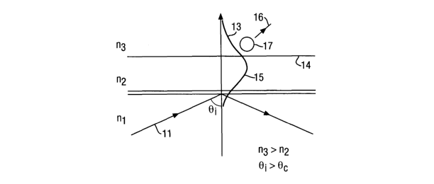
Referring now to Figure 2, a "leaky" waveguide structure is based an a similar
arrangement in which the refractive indices nl and n2 of the media are
"snatched" so
that at a certain angle or angles B; not all the incident light is reflected.
Total internal
reflection is now "frustrated" and a proportion of the light is coupled,
without
generating an evanescent field, from the optically denser medium to the
optically less
dense medium.
Where the optically less dense medium is in contact with a fiuther medium of
lower
refractive index n3 the coupled light will be returned by total internal
reflection at the
interface 14 between the two media. It will be apparent therefore, that
because only a
proportion of light is coupled back to the optically denser medium, an optical
mode 15
is propagated within the optically less dense medium. It will further be
realised that
the optical mode 15 includes an associated evanescent field 13, which
propagates in
the medium of lower refractive index.
The optical mode 15 and its associated evanescent field 13 are sensitive to
changes in
the refractive index of the medium of lower refractive index and can excite
scattering
or emission of light 16 by particles 17 in the vicinity. It will be apparent
that, because
the intensity of scattered or emitted light is dependent on the intensity of
the
evanescent field, the particle 17 is more strongly illuminated the greater the
depth of
penetration of the evanescent field 13.
CA 02501267 2005-04-04
WO 2004/031743 PCT/GB2002/004545
14
Referring now to Figure 3 a leaky waveguide structure according to the present
invention comprises a chip, generally designated 18 comprising an upper
surface of a
300 nm silica sol layer 19 (n = 1.43) provided on a thin layer (8.5 nm) of
titanium 20
coating a 1 mm glass substrate layer 21 (n = 1.5). The thickness and
refractive index
of the silica sol layer 19 is chosen to support a single sharp-guided optical
mode 15 at
a wavelength of incident light of 685 nm or 488 nm and to optimise the depth
of
penetration (about 1.5 -2.0 Vim) of the evanescent field.
The sensing layer 22 can comprise a layer of a biochemical sample to be
analysed.
Alternatively or in addition, the sensing layer 22 can comprise an aa~.tibody
layer
deposited on the silica sol layer 19 of the chip 18 by soaking in 10% 3-
aminopropyltriethoxysilane (APTS) for 4 h, washing with ethanol and drying at
110°C for 2h. The chip 18 is then activated for detection of Bacillus
globigii by
soaking with 5% aqueous glutaraldehyde for 30 min followed by cxposure with
suitable antibody solution of concentration 300 ,ug ml-1 in 10 mM phosphate
buffer
(pH 7.4) for 30 min. Finally, unreacted sites on the chip 18 are blocked by
exposure
of the chip 18 within the flow cell to 5 mg ml-1 aqueous bovine serum albumin
(BSA).
Figure 4 shows the optical mode supported in the silica sol layer 19 of the
chip 18
including its associated evanescent field 13. As may be seen, the mode 15 is a
single
sharp guided mode in which the depth of penetration of the evanescent field 13
extends to overlap a particle in the sensing layer 22.
Referring now to Figure 5, the change in reflectivity of the waveguide as a
function of
the distance between the upper surface of the chip 18 and the bound bacterium
is
CA 02501267 2005-04-04
WO 2004/031743 PCT/GB2002/004545
compared with change in the reflectivity of commonly used SPR and resonant
mirror
structures. As may be seen the change in reflectivity of the waveguide
structure is far
greater for the MCLW structure compared to SPR and resonant mirror structures,
suggesting a greater extension of the evanescent field 13 and better detection
of large
5 particles 19 such as bacteria.
Refernng now to Figure 6, an optical sensor 23 suitable for detection of
particles 19
by fluorescence comprises an air-cooled argon ion laser 24 (162LGL, Laser
Graphics
GmbH, Germany) with an emission wavelength of 488 nm at 10 mW power. A 488
10 +/- 5 nm filter 25 (Glen Spectra, UK) is mounted in front of the laser to
remove
unwanted emissions at different wavelengths. The light is directed to a BK7
prism 26
where a proportion is coupled into the chip 18 by adjustment of mirrors 27.
The chip 18 is associated with or placed within a Perspex~ flow cell (not
shown) of
15 internal diameter of about 15 mm and inlet ports diametrically opposed. A
peristaltic
pump (MlI~IIPLUS-3, MP4, Canada) pumps a fluid containing particles to be
analysed
to the flow cell at a rate S00 ~,l miri 1. The pump and the chip 18 are
arranged so that
the direction of propagation of the leaky wave mode opposes the direction of
flow of
the fluid.
Light 16 emitted from the particles 17 by interaction with the evanescent
field 13 is
collected by a very high-resolution digital camera 28 (PULNIXTM-IOOl, USA)
comprising a 1" monochrome progressive scanning 1024 (H) x 1024(V) interline
transfer CCI~ imager. An emission filter 29 is provided above the chip to
filter
scattered light from emitted light (a 505 nm long pass filter, Comar UK) or to
filter
CA 02501267 2005-04-04
WO 2004/031743 PCT/GB2002/004545
16
emitted light from scattered light (interference band pass filter for 488 nm,
Comar,
UK). The intensity of fluorescence of a particular particle 19 is calculated
by
summation of all pixels belonging to that particle whose value exceeds a
predetermined threshold value.
The proportion of light reflected by the chip is collected at a second
detector (not
shown) which can be used to monitor the reflectivity of the chip so as to
maintain the
incident light at the resonant angle. Figure 7 illustrates the peak in the
reflectivity of
the waveguide structure of Figure 3, which occurs at an angle of incidence of
about
63°.
Scattering and fluorescence observations were investigated using the sensor of
Figure
6 for a number of particles, including latex beads, yeast cells, and Bacillus
globiggi
spores:
Figure 8 a) shows a background image of the MCLW chip. As may be seen the
MCLW chip has a smooth surface with no significant imperfections such as pits
or
scratches that could cause scattering of light and confuse the detection of
particles.
The smooth surface of the MCLW chip 18 is particularly advantageous in that
the
necessity for a subtraction of the background image from the test image is
obviated.
Figures 8 b) and c) show scattering of light observed from latex beads of
diameter
1.09 lCm at a concentration 10~ beads ml-1 in respectively full flow or a stop-
start flow
mode. As may be seen, the scattering of light from the beads is improved in
the stop-
CA 02501267 2005-04-04
WO 2004/031743 PCT/GB2002/004545
17
start flow mode suggesting that the particles as settle downwards onto the
sensing
layer the greater their overlap of the evanescent field. -
Figures 9 a) and b) show respectively fluorescence and scattering images
obtained
from 100% fluorescein labelled 5 ,um latex beads (Sigma, LTK) at the same
concentration and conditions as for Figure 8. However, for fluorescence the
laser is
operated at 10 mW power and for scattering the laser is operated at 4 mW power
with
a simple blue filter place in front of the camera .
Figures 10 a) to d) show images comparing scattering and fluorescence
observations
for 100% and 10% fluorescein labelled 2.5 ~,m latex beads (Sigma, Ul~) at 10
mW
power. As may be seen from figures b) and d) the fact that the scattering
images from
the beads are approximately the same whilst the fluorescence images (C~gures
a) and
c)) are markedly different suggests a low level of cross talk interference
between the
types of images.
Figures 11 a) and b) show respectively the fluorescence and scattering images
from
labelled yeast cells. The yeast cells, SacclZaYOmyces cerevisiae (UM:1'ST,
11I~) are
genetically modified to express GFP, a green fluorescent protein obtained from
Aequorea victoria, during repair of DNA damage and have a peak excitation
wavelength of 490 nm and a peak emission wavelength of 517 nm. The cells were
activated to express GFP by exposure to methyl methanesulphonate - a known DNA
damaging compound. As may be seen the fluorescence images are inferior, even
at
10 mW power, to the scattering images suggesting that the only yeast cells
producing
levels of GFP are detected. Further comparison of Figure 11 a) with Figure 10
a)
CA 02501267 2005-04-04
WO 2004/031743 PCT/GB2002/004545
18
suggests that the percentage of yeast cells expressing high levels of
fluorescein is
lower than 2.5%. Further the images of the yeast obtained suggest that they
varyrhi
size between 3 to 8 ~.m according to their stage in the cell cycle. Comparison
of
Figure 11 b) with Figure 10 b) clearly shows that detection of yeast cells by
scattering
of light is also more difficult than detection of latex beads. This may be
attributable to
the fact that latex beads have a higher refractive index than yeast cells arid
so scatter
light more strongly.
Exposure of the sensor to Bacillus globiggi spores (CAMR, UI~) revealed the
spores
as areas of diffuse light moving across the surface of the chip. Where the
spores
appeared to move close to the surface of the chip they were observed ot~
occasion to
come to an instantaneous stop being presumably captured by an antibody. Such
behaviour was not observed when the sensor was coated with a surface
comprising
BSA rather than antibody. Again the stop start flow mode appeared to allow
settling
of the spores onto the chip where the images became brighter and more well
defined .
Figure 12 shows the scattering image obtained after exposure of the chip to
Bacillus
globiggi spores at a concentration of 107 spores ml-t for 1 h. It will be
realised that
the response of the MCLW sensor compares favourably with SPR sensors, which
generally require concentrations of Bacillus globiggi of 109 spores per ml-t
for
adequate detection.
The scattering intensity was compared with the scattering intensity when the
spores
are exposed to an SPR sensor. The results are summarised in Table 1. As may be
seen, the scattering intensity from the MCLW chip is about three times as
strong as
the scattering intensity from the SPR chip. The standard deviation in the
experimental
CA 02501267 2005-04-04
WO 2004/031743 PCT/GB2002/004545
19
results is higher in the case of the MCLW chip since the depth of penetration
of the
evanescent field is higher and although the probability of overlap with the
particles
higher they are also detectable at larger distances from the chip surface.
Type of chip Intensity of Scattering Intensity of Scattering
(before settling) (after settling)
SPR 45 +/- 9% 73 +/- 2%
MCLW 125 +/-15% 192 +/- 4%
Table 1
These results show that a MCLW sensor has been developed, based on flue
scattering
or emission of light, which is capable of detecting particles and more
sensitive than
other currently used sensors. The sensor increases the depth of penetration of
an
evanescent field from the sensor surface into the sample and the extent o ('
propagation
of the mode thus providing an effective interrogation for the detection of
particles.