Note: Descriptions are shown in the official language in which they were submitted.
CA 02501358 2005-03-18
IMAGE FORMING APPARATUS AND PROCESS CARTRIDGE
BACKGROUND OF THE INVENTION
Field of the invention
This invention is related to image forming apparatuses and process
cartridges.
Description of the related art
The electrophotography is used in electrophotographic apparatuses such
as copy machines and laser beam printers since the electrophotography enables
high-speed, high-quality printing.
In general, the photoreceptors used in the electrophotographic
apparatuses have been organic photoreceptors containing photoconductive
organic materials, recently. Regarding the constitutions of the
photoreceptors,
separated function photoreceptors have been used in which a charge generating
material and a charge transfer material are dispersed in different layers
(charge
generating layer and charge transfer layer).
In recent years, office functions have been improved in quality and in
speed; there have been demands for faster and colorized document processing
and faster, colorized, high-quality image forming apparatuses (copying
1
CA 02501358 2005-03-18
machines, printers, facsimile machines, etc.) for processing the documents. In
order to satisfy the demands, tandem-type color image forming apparatuses have
been proposed and commercialized. A tandem-type color image forming
apparatus has separate image forming units for respective colors of black (K),
yellow (Y), magenta (M), and cyan (C). The tandem-type color image forming
apparatus forms images of different colors in the respective image forming
units,
then transfers the images onto a transfer member or an intermediate transfer
member so that the images overlap, thus forming a color image.
In the color image forming apparatuses, techniques have been proposed
(for example in Japanese Patent Application Laid-0pen (JP-A) No. 2003-
241551) which can switch between different image formation modes in
accordance with the image and the kind of the image receiving medium, thus
realizing high quality and high efficiency. For example, only the black toner
is
used when black-and-white image is formed, whereby the process speed can be
supposedly higher than in the color image formation. A high-quality image can
supposedly be formed by lengthening the time required for the image formation
when the image receiving medium is heavy paper or an OHP sheet, in both cases
of color image forming apparatuses and monochromatic image forming
apparatuses.
However, if the time required for the processes from charging to
development varies as in the above techniques, the image quality tends to be
insufficient. When the image formation mode is switched to another image
formation mode, the time required for the processes from charging to
development changes, but photoreceptors sufficiently adaptable to the change
in
the use condition have not been developed. Therefore, in such techniques,
2
CA 02501358 2005-03-18
there have been a problem that, when image formation is conducted in a process
condition in which a longer time is required for the processes from charging
to
development, fogging and black spots develop severely and image memory
easily occurs.
SUMMARY OF THE INVENTION
The invention has been made in consideration of the above problems of
the conventional techniques.
An aspect of the invention is to provide an image forming apparatus
comprising an electrophotographic photoreceptor, a charging unit, an exposure
unit, a development unit, and a transfer unit. The image forming apparatus
conducts charging, exposure, development, and transfer while moving the
circumferential surface of the electrophotographic photoreceptor in a
predetermined direction. The image forming apparatus further comprises a
controlling unit. The controlling unit controls the moving velocity of the
circumferential surface of the electrophotographic photoreceptor so that the
time
required for the processes from charging to development is changeable. The
electrophotographic photoreceptor includes an undercoat layer and a
photosensitive layer. The undercoat layer includes a metal oxide particle and
an acceptor compound having a group capable of reacting with the metal oxide
particle.
When the image forming apparatus of the invention is used, the
electrophotographic characteristic of the electrophotographic photoreceptor is
sufficiently high even when the time required for the processes from charging
to
3
CA 02501358 2005-03-18
development is long. Accordingly, the image formation can be conducted in
various conditions when the image forming apparatus of the invention is used.
This effect is caused by the inclusion of the acceptor compound having a group
capable of reacting with the metal oxide particle in the undercoat layer. Even
when the time required for the processes from charging to development is
varied
in the image forming apparatus of the invention, the development of the
fogging
and black spots on the obtained image and the image memory can be sufficiently
suppressed.
The inventors suppose that the reason why the above effects are obtained
is as described below.
First, the reason why the conventional image forming apparatuses have
the above problems is described. The undercoat layer used in a conventional
electrophotographic receptor is obtained by: dispersing metal oxide pigments
and a binder resin in a solvent and applying the obtained dispersing liquid.
If
the thickness of the undercoat layer is larger than 5 pm, a large amount of
metal
oxide particles are incorporated into the undercoat layer in order to form a
conductive path which secures a sufficient charge transporting ability in the
undercoat layer. In this case, a part of the metal oxide particles are not
covered
by the binder resin but exposed. The exposed metal oxide particles form a
charge injection site. The charge injection site works as the point at which
charge is injected to the upper layer. When the processes from charging to
development take a long time, the charge injected to the upper layer can move
to
the surface of the photoreceptor and cancel the surface charge to cause
fogging
or black spots. If the resistance of the undercoat layer is excessively low,
the
charge injection to the upper layer occurs intensely to cause severe fogging.
4
CA 02501358 2005-03-18
On the other hand, when the resistance of the undercoat layer is excessively
high,
the image defects such as fogging can be prevented; however, the charge tends
to accumulate in the undercoat layer or on the interface between the undercoat
layer and the upper layer, whereby the residual potential becomes high owing
to
the charge accumulated during continuous or longtime use. The high residual
potential causes defects in the image density, thereby deteriorating the image
quality.
Accordingly, the undercoat layer has to have both of the resistance
controlling function and the charge injection controlling function. This
requirement have imposed a tight restriction to the design.
As the result of the intensive study carried out by the inventors of the
present invention, the following advantages of the electrophotographic
photoreceptor of the invention have been found. The electrophotographic
photoreceptor of the invention has an undercoat layer including a metal oxide
particle and an acceptor compound having a group capable of reacting with the
metal oxide particle. When the photoreceptor of the invention is used in the
image forming apparatus of the invention, it is possible to prevent the
accumulation of the charge in the undercoat layer and the accumulation of the
charge in the neighborhood of the interface between the undercoat layer and
the
upper layer. Therefore, in the image forming apparatus of the invention,
potential defects such as the decrease in electric potential during repetitive
use
is prevented, and it is possible to conduct sufficient and uniform charging.
Because of the above advantages, the image forming apparatus of the
invention realizes better electric characteristics and image quality
characteristics than conventional image forming apparatuses can realize. Even
CA 02501358 2005-03-18
if the time required for the processes from charging to development is
changed,
the fogging and black spots of the obtained image, and the image memory are
sufficiently suppressed. Even if the image forming apparatus is used
continuously for a long time, the variation in the electric characteristics is
small
and it is possible to sufficiently suppress the occurrence of the image
density
defect.
Accordingly, formation of high-quality image and long life are realized
by the image forming apparatus of the invention, whereby the invention has
been made.
An aspect of the invention is to provide an image forming apparatus
comprising an electrophotographic photoreceptor, a charging unit, an exposure
unit, a development unit, and a transfer unit, wherein:
the image forming apparatus conducts charging, exposure, development,
and transfer while moving the circumferential surface of the
electrophotographic
photoreceptor in a predetermined direction;
the image forming apparatus further comprises a controlling unit which
controls the moving velocity of the circumferential surface of the
electrophotographic photoreceptor so that the time required for the processes
from charging to development is changeable;
the electrophotographic photoreceptor includes an undercoat layer and a
photosensitive layer; and
the undercoat layer includes a metal oxide particle and an acceptor
compound having a group capable of reacting with the metal oxide particle.
Another aspect of the invention is to provide a color image forming
apparatus comprising a plurality of image forming units, wherein:
6
CA 02501358 2005-03-18
each image forming unit includes an electrophotographic photoreceptor,
a charging unit, an exposure unit, a development unit, and a transfer unit;
each image forming unit conducts charging, exposure, development, and
transfer while moving the circumferential surface of the electrophotographic
photoreceptor in a predetermined direction;
each image forming unit further includes a controlling unit which
controls the moving velocity of the circumferential surface of the
electrophotographic photoreceptor so that the time required for the processes
from charging to development is changeable;
the electrophotographic photoreceptor includes an undercoat layer and a
photosensitive layer; and
the undercoat layer includes a metal oxide particle and an acceptor
compound having a group capable of reacting with the metal oxide particle.
Another aspect of the invention is to provide a process cartridge
comprising an electrophotographic photoreceptor and at least one selected from
the group consisting of a charging unit, a development unit, a transfer unit,
and
a cleaning unit, wherein:
the process cartridge is attachable to an image forming apparatus and
detachable from the image forming apparatus;
the image forming apparatus conducts charging, exposure, development,
and transfer while moving the circumferential surface of the
electrophotographic
photoreceptor in a predetermined direction;
the process cartridge further includes a controlling unit which controls
the moving velocity of the circumferential surface of the electrophotographic
photoreceptor so that the time required for the processes from charging to
7
CA 02501358 2005-03-18
development is changeable;
the electrophotographic photoreceptor includes an undercoat layer and a
photosensitive layer; and
the undercoat layer includes a metal oxide particle and an acceptor
compound having a group capable of reacting with the metal oxide particle.
In all the aspects, the following constitution may be selected.
The controlling unit may be such a controlling unit that the controlling
unit can control the moving velocity of the circumferential surface of the
electrophotographic photoreceptor while satisfying the conditions represented
by the following formulae (1) and (2) and that the controlling unit can switch
among a plurality of control modes including a normal mode, a low-speed mode,
and a high-speed mode.
Formula (1): T,aW >_ (1/3) T
Formula (2): T,,;g,, <_ 3T
(In the formulae, T represents the time between charging and
development in the electrophotograhic process in the normal mode; T,oW
represents the time between charging and development in the
electrophotographic process in the low-speed mode; and T,,;g,, represents the
time
between charging and development in the electrophotographic process in the
high-speed mode.)
The acceptor compound may be a compound having an quinone group.
The acceptor compound may be a compound having an anthraquinane structure.
The acceptor compound may be selected from anthraquinone,
hydroxyanthraquinone, aminoanthraquinone, and aminohydroxyanthraquinone.
In an embodiment, the metal oxide particle has been subjected to a
8
CA 02501358 2005-03-18
surface treatment with a coupling agent. The coupling agent may be a silane
coupling agent. The silane coupling agent may have an amino group.
The metal oxide particle may be selected from titanium oxide, zinc
oxide, tin oxide, and zirconium oxide.
The electrophotographic photoreceptor may have an outermost layer
including an organic or inorganic particle. The particle in the outermost
layer
may be a fluorine-containing resin particle.
The charge generating layer of the electrophotographic photoreceptor
may include a phthalocyanine pigment or an azo pigment. The charge
generating layer may include a hydroxygallium phthalocyanine pigment, a
chlorogallium phthalocyanine pigment, an oxytitanyl phthalocyanine pigment,
or a non-metallic phthalocyanine pigment.
The charging unit may be a contact charging unit which charge the
electrophotographic photoreceptor by contacting the electrophotographic
photoreceptor.
The transfer unit may use the intermediate transfer method in which a
toner image formed on the circumferential surface of the electrophotographic
photoreceptor is transferred indirectly to an image receiving medium via an
intermediate transfer member.
BRIEF DESCRIPTION OF THE DRAWINGS
Fig. 1 is a schematic constitutional diagram illustrating an embodiment
of the image forming apparatus of the invention.
Fig. 2 is a schematic cross-sectional view illustrating an example of the
9
CA 02501358 2005-03-18
electrophotographic photoreceptor of the invention.
DESCRIPTION OF THE PRESENT INVENTION
Preferable embodiments of the invention will be explained in detail,
occasionally referring to the figures. In the figures, the same or
corresponding
members are designated by the same sign, and overlapping descriptions are
omitted.
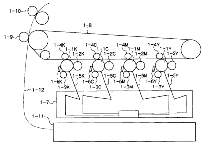
Fig. 1 is a schematic constitutional diagram illustrating an embodiment
of the image forming apparatus of the invention. The image forming apparatus
shown in Fig. 1 is a so-galled tandem type digital color printer. In the image
forming apparatus, respective image forming units for yellow (Y), magenta (M),
cyan (C), and black (K) are disposed in parallel. Each image forming unit
includes an electrophotographic photoreceptor (occasionally called
"photoreceptor" hereinafter). The photoreceptor is held such that the
photoreceptor can be rotated in a predetermined direction. The image forming
unit further includes a developing unit, a charging roll, a primary transfer
roll,
an exposure unit, and a cleaning blade disposed along the moving direction of
the circumferential surface of the photoreceptor. In the image forming unit,
the
photoreceptor after charging can be irradiated with the laser light emitted by
an
ROS (Raster Output Scanner) 1-7 as the exposure unit. For example, the image
forming unit for black (K) comprises a photoreceptor 1-1K, a developing unit
1-2K, a charging roll 1-3K, a primary transfer roll 1-4K, and a cleaning blade
1-6K. The photoreceptor 1-1K after charging can be irradiated with an
exposure light 1-SK.
CA 02501358 2005-03-18
Each of the photoreceptors 1-1 Y, 1-1 M, 1-1 C, and 1-1 K comprises a
conductive support, an undercoat layer, and a photosensitive layer. The
undercoat layer and the photosensitive layer are disposed on the conductive
support. The undercoat layer includes a metal oxide particle and an acceptor
compound having a group capable of reacting with the metal oxide particle.
The details of the photoreceptor will be described later.
Each photoreceptor is connected to a driving unit, though the details are
not shown in the figures. The driving unit has a controlling function of
controlling the rotating velocity (the moving velocity of the circumferential
surface) of the photoreceptor. In each image forming unit, the driving unit
can
change the time required for the processes from charging to development owing
to the controlling function. Owing to the controlling function, the image
forming unit can switch among a plurality of control modes including a normal
mode, a low-speed mode, and a high-speed mode and conduct the image
formation in the selected control mode.
For example, in the formation of a black image: the photoreceptor 1-1 K
is charged by the charging roll 1-3K to which an electric potential is
applied;
then the photoreceptor 1-1K is imagewise exposed to the laser light 1-SK
emitted by the ROS (Raster Output Scanner) 1-7 to form a latent image; then
the
developing unit 1-2K develops the image with toner; then the toner image is
transferred to an intermediate belt 1-8 by the electric field of the primary
transfer roll 1-4K; then the toner image is further transferred to a recording
medium fed from a paper tray 1-11, by the electric field of the secondary
transfer roll 1-9; then the toner image is thermally fixed in a fixing unit 1-
10,
whereby the recording medium on which the image is formed is discharged.
11
CA 02501358 2005-03-18
The color image formation in the normal mode is conducted through the
following processes: in the image forming unit for yellow (Y), the
photoreceptor
1-lY is charged by the charging roll 1-3Y to which an electric potential is
applied; then the photoreceptor 1-lY is imagewise exposed to the laser light 1-
SY emitted by the ROS (Raster Output Scanner) 1-7 to form a latent image; then
the developing unit 1-2Y develops the image with toner; then the toner image
is
transferred to an intermediate belt 1-8 by the electric field of the primary
transfer roll 1-~Y; then, similar processes are sequentially conducted in the
respective image forming units for magenta (M), cyan (C), and black (B), so
that
a color toner image is formed on the intermediate transfer belt by the
multiple
transfers; then the toner image is further transferred to a recording medium
fed
from a paper tray 1-11, by the electric field of the secondary transfer roll 1-
9;
then the toner image is thermally fixed in a fixing unit 1-10, whereby the
recording medium on which the image is formed is discharged. Reference
number 1-12 represents a path of paper transfer.
The rotating velocity of the photoreceptor in the normal mode is not
particularly restricted. In a preferable embodiment, the rotating velocity is
set
such that the time required for the processes from charging to development in
each image forming unit is 50 msec to 300 msec.
When the recording medium fed from the paper tray is thick paper or an
OHP sheet, it is preferable to switch the image formation mode to the low-
speed
mode. In the low-speed mode, the rotating velocity of the photoreceptor 1-1 in
each unit is low, the time required for the processes from charging to
development is elongated, and the fixing time is long enough to fix the
developer onto the thick paper or the OHP sheet sufficiently. The image
12
CA 02501358 2005-03-18
formation procedures in the low-speed mode is the same as the procedures in
the
normal mode described above. The rotating velocity (the moving velocity of
the circumferential surface) of the photoreceptor in the low-speed mode is not
particularly limited, and preferably satisfies the following formula (1).
Formula (1): T,oW >_ (1/3) T
(In the formula, T represents the time between charging and
development in the electrophotograhic process in the normal mode; and T,oW
represents the time between charging and development in the
electrophotographic process in the low-speed mode.)
When a monochromatic image (black-and-white image) is printed, the
following processes are conducted in the image forming unit for black (K): the
photoreceptor 1-1K is charged by the charging roll 1-3K to which an electric
potential is applied; then the photoreceptor 1-1K is imagewise exposed to the
laser light 1-SK emitted by the ROS (Raster Output Scanner) 1-7 to form a
latent
image; then the developing unit 1-2K develops the image with toner; then the
toner image is transferred to an intermediate belt 1-8 by the electric field
of the
primary transfer roll 1,4K; then the toner image is further transferred to a
recording medium fed from a paper tray 1-11, by the electric field of the
secondary transfer roll 1-9; then the toner image is thermally fixed in a
fixing
unit 1-10, whereby the recording medium on which the image is formed is
discharged. In the formation of the monochromatic image, the image formation
mode may be switched to the high-speed mode, so that the rotating velocity of
the photoreceptor 1-1K is increased and the time required for the processes
from
charging to development is shortened. The rotating velocity (the moving
velocity of the circumferential surface) of the photoreceptor in the high-
speed
13
CA 02501358 2005-03-18
mode is not particularly limited, and preferably satisfies the following
formula
(2).
Formula (2): Th;gh <_ 3T
(In the formula, T represents the time between charging and
development in the electrophotograhic process in the normal mode; and Th;gn
represents the time between charging and development in the
electrophotographic process in the high-speed mode.)
When the undercoat layers of the photoreceptors 1-lY, 1-1M, 1-1C, and
1-1K of the tandem-type color image forming apparatus each include a metal
oxide particle and an acceptor compound having a group capable of reacting
with the metal oxide particle, the electrophotographic characteristic of the
photoreceptors are sufficiently heightened and the use condition thereof can
be
selected from a broader range. Therefore, even when the image formation
mode is switched among the normal mode, the high-speed mode, and the low-
speed mode (whereby the image formation is conducted with different lengths of
time between charging and development), it is possible to sufficiently
suppress
the occurrence of the fogging and black spots in the obtained image and the
occurrence of the image memory.
In the following, the elements of the image recording apparatus of the
invention are described.
The structure of the photoreceptor is described first. Fig. 2 is a
schematic cross-sectional view of an example of the electrophotographic
photoreceptor of the image forming apparatus of the invention. An
electrophotographic photoreceptor 1-1 has a structure in which an undercoat
layer 2, an intermediate layer 4, a photosensitive layer 3, and a overcoat
layer 5
14
CA 02501358 2005-03-18
are successively laminated on a conductive support 7. The electrophotographic
photoreceptor shown in 1-1 is a separated-function photoreceptor; therefore
the
photosensitive layer 3 is comprised of a charge generating layer 31 and a
charge
transporting layer 32.
The conductive support 7 may be selected from: metal drums made of
metals such as aluminum, copper, iron, stainless-steel, zinc, and nickel;
supports
obtained by vapor-iiepositing metals such as aluminum, copper, gold, silver,
platinum, palladium, titanium, nickel-chrome, stainless-steel, and indium onto
base materials such as sheets, paper, plastics, and glass; supports obtained
by
vapor-depositing conductive metal compounds such as indium oxide and tin
oxide onto base materials such as sheets, paper, plastics, and glass; supports
obtained by laminating metal foil on the above base materials; conductive
supports obtained by coating the above base materials with coating liquids
each
prepared by dispersing, in a binder resin, carbon black, indium oxide, tin
oxide,
antimony oxide powder, metal powder, copper iodide, or the like.
The shape of the conductive support 7 is not limited to a drum shape, but
may be, for example, a sheet shape or a plate shape. When the conductive
support 7 is a metal pipe, the surface of the metal pipe may be unprocessed,
or
may be subjected to mirror grinding, etching, anodization, rough grinding,
centerless grinding, sandblast, or wet honing.
The undercoat layer 2 includes a metal oxide particle and an acceptor
compound having a group capable of reacting with the metal oxide particle.
The metal oxide particle used in the invention has to have a powder
resistance of 10z to 10" S2~cm. This is because the undercoat layer must have
an appropriate resistance in order to have a leak resistance. The metal oxide
CA 02501358 2005-03-18
particle is preferably a metal oxide particle having a resistance in the above
range which particle is selected from a metal titanium oxide particle, a zinc
oxide particle, a tin oxide particle, and a zirconium oxide particle. A zinc
oxide particle is particularly preferable. When the resistance of the metal
oxide particle is lower than the above range, the leak resistance is
insufficient.
When the resistance of the metal oxide particle is higher than the above
range,
the residual potential tends to increase. In an embodiment, two or more kinds
of metal oxide particles are used each of which is different in particle
diameter
and/or in the surface treatment to which the kind of metal oxide particle has
been subjected. The metal oxide particle has a specific surface of preferably
lOm2/g or higher. When the specific surface is lower than lOm2/g, the charging
property tends to be insufficient and an excellent electrophotographic
characteristic is unlikely to be obtained.
In an embodiment, the metal oxide particle has been subjected to a
surface treatment. Any known surface treating agent may be used as long as
the surface treating agent can provide the desired properties. For example,
the
surface treating agent may be selected from a silane coupling agent, a
titanate
coupling agent, an aluminum coupling agent and a surfactant. In particular, a
silane coupling agent is preferable since the silane coupling agent provides a
satisfactory electrophotographic characteristic. The silane coupling agent
preferably has an amino group since such a silane coupling agent provides an
excellent blocking property to the undercoat layer.
The silane coupling agent having an amino group is not particularly
limited as long as the resultant electrophotographic photoreceptor has the
desired characteristics. Specific examples thereof include (but not limited
to)
16
CA 02501358 2005-03-18
y-aminopropyltriethoxysilane, N-(3-(aminoethyl)fy-aminopropyl
trimethoxysilane, N-(3-(aminoethyl)-~~minopropylmethyl methoxysilane and
N,N--bis((3-hydroxyethyl)~y-aminopropyl triethoxysilane.
In an embodiment, a mixture of two or more silane coupling agents is
used. Examples of silane coupling agents that can be used in combination with
the silane coupling agent having an amino group include vinyltrimethoxysilane,
y-methacryloxypropyl tris(~i-methoxyethoxy)silane, (3-(3,4-
epoxycyclohexyl)ethyl trimetoxysilane, y-glycidoxypropyl trimethoxysilane,
vinyltriacetoxysilane, y-mercaptopropyltrimethoxysilane, y-
aminopropyltriethoxysilane, N-(3-(aminoethyl)~y-aminopropyl trimethoxysilane,
N-(3-(aminoethyl)~-aminopropylmethyl methoxysilane, N,N-bis(~3-
hydroxyethyl)-~y-aminopropyl triethoxysilane, and y-
chloropropyltrimethoxysilane; but these examples are not restrictive.
Any known surface treatment method may be employed. The surface
treatment method may be a dry method or a wet method.
When the surface treatment method is a dry method, the dry method may
comprise: dropwise adding a silane coupling agent as it is or in the form of a
solution in an organic solvent to the metal oxide particle while the metal
oxide
particle is agitated with a mixer or the like having a high shearing force;
and
spraying the metal oxide coated with the silane coupling agent with dry air or
nitrogen gas. This dry method enables a uniform surface treatment. The
addition or spraying is preferably conducted at a temperature which is lower
than the boiling point of the solvent. When the spraying is conducted at a
temperature which is not lower than the boiling point of the solvent, the
solvent
evaporates before the silane coupling agent is uniformly mixed with the metal
17
CA 02501358 2005-03-18
particle by the agitation and the silane coupling agent locally aggregate,
whereby the surface treatment is unlikely to be uniform. In an embodiment,
the metal oxide particle is baked at a temperature of 100 QC or higher after
the
addition or the spraying. The conditions (such as the temperature and the
baking time) of the baking is not particularly limited as long as the
resultant
photoreceptor has the desired electrophotographic characteristic.
When the surface treatment method is a wet method, the wet method
may comprise: dispersing the metal oxide particle in a solvent by agitatation,
an
ultrasonic wave, a sand mill, an attriter or a ball mill; then adding a
solution of a
silane coupling agent to the metal oxide particle dispersion liquid,
dispersing
the silane coupling agent and the metal oxide in the mixture liquid by
agitation;
and removing the solvent. This wet method enables a uniform surface
treatment. The removal of the solvent may be conducted by filtration or
distillation. In an embodiment, the metal oxide particle is baked at a
temperature of 100 ~C or higher after the removal of the solvent. The
conditions (such as the temperature and the baking time) of the baking is not
particularly limited as long as the resultant photoreceptor has the desired
electrophotographic characteristic. In the wet method, it is also possible to
eliminate the moisture contained in the metal oxide particle prior to the
addition
of the surface treating agent. The elimination of the moisture may be
conducted, for example by: heating the metal oxide particle in the solvent for
the surface treatment while agitating the solvent; or utilizing the azeotropy
with
the solvent.
The amount of the silane coupling agent relative to the metal oxide
particles in the undercoat layer may be selected arbitrarily as long as the
desired
18
CA 02501358 2005-03-18
electrophotographic characteristic can be obtained.
The acceptor compound may be any compound having a group capable
of reacting with the metal oxide particle as long as the desired
characteristics
can be obtained. The acceptor compound is preferably a compound having a
hydroxyl group. The acceptor compound is more preferably a compound
having a hydroxyl group and an anthraquinone structure. The compound
having a hydroxyl group and an anthraquinone structure may be a
hydroxyanthraquinone compound or an aminohydroxyanthraquinone compound.
More specifically, the compound is preferably alizarin, quinizarin,
anthrarufin,
or purpurin.
The amount of the acceptor compound to be used in the invention is not
particularly limited as long as the desired characteristics can be obtained.
The
amount of the acceptor compound is preferably 0.01 to 20 % by weight based on
the weight of the metal oxide particles, more preferably 0.05 to 10 % by
weight
based on the weight of the metal oxide particles. When the amount of the
acceptor compound is smaller than 0.01 % by weight based on the weight of the
metal oxide particles, the obtained acceptor property is insufficient for
contributing to the improvement of the charge accumulation in the undercoat
layer, whereby the durability is likely to be deteriorated; for example, the
residual potential tends to increase during repetitive use. When the amount of
the acceptor compound is larger than 20 % by weight based on the weight of the
metal oxide particles, the metal oxide particles aggregate easily and the
metal
oxide particles fail to form an excellent conductive path in the undercoat
layer
upon the formation of the undercoat layer, whereby image quality defects such
as black spots are likely to occur and the durability is likely to be
deteriorated;
19
CA 02501358 2005-03-18
for example, the residual potential tends to increase during repetitive use.
The binder resin contained in the undercoat layer 2 may be any known
resin as long as the resin can form an excellent film and provide the desired
characteristics. The binder resin may be a known polymer resin, which may be
a charge transporting resin having a charge transporting group or a conductive
resin such as polyaniline. Examples of the polymer resin include acetal resins
such as polyvinylbutyral, polyvinyl alcohol resins, casein, polyamide resins,
cellulose resins, gelatin, polyurethane resins, polyester resins, methacrylic
resins, acrylic resins, polyvinyl chloride resins, polyvinyl acetate resins,
vinyl
chloride-vinyl acetate-malefic anhydride resins, silicone resins, silicone-
alkyd
resins, phenolic resins, phenol-formaldehyde resins, melamine resins, and
urethane resins. The resin is preferably a resin which is insoluble in the
solvent used for the application of the upper layer. The resin is more
preferably a phenolic resin, a phenol-formaldehyde resin, a melamine resin, an
urethane resin or an epoxy resin.
In the coating liquid for forming the undercoat layer 2, the ratio of the
metal oxide fine particles to the binder resin is not particularly limited as
long
as the resultant electrophotographic photoreceptor has the desired
characteristics.
The coating liquid for forming the undercoat layer 2 may further include
various additives for the purpose of improving the electric characteristics,
the
environmental stability and the image quality.
Examples of the additives include: electron transporting substances such
as quinone compounds (such as chloranil and bromoanil),
tetracyanoquinodimethane compounds, fluorenone compounds (such as 2,4,7-
CA 02501358 2005-03-18
trinitrofluorenone and 2,4,5,7 tetranitro-9-fluorenone), oxadiazole compounds
(such as 2-(4-biphenyl)-5-(4-t-butylphenyl)-1,3,4-oxadiazole, 2,5-bis(4-
naphthyl)-1,3,4-oxadiazole, and 2,5 bis(4-diethylaminophenyl)-1,3,4-
oxadiazole), xanthone compounds, thiophene compounds, and diphenoquinone
compounds (such as 3,3',5,5'-tetra-t butyldiphenoquinone); electron
transporting pigments such as condensed polycyclic electron transporting
pigments and azo electron transporting pigments; and other known substances
such as zirconium chelate compounds, titanium chelate compounds, aluminum
chelate compounds, titanium alkoxide compounds, organic titanium compounds,
and silane coupling agents.
A silane coupling agent is used for the surface treatment of zinc oxide.
In addition, a silane coupling agent may be also included in the coating
liquid as
an additive. Examples of the silane coupling agent as the additive include
vinyltrimethoxysilane, y-methacryloxypropyl-tris(~3-methoxyethoxy)silane, (3-
(3,4-epoxycyclohexyl)ethyl trimethoxysilane, y-glycidoxypropyl
trimethoxysilane, vinyltriacetoxysilane, y-mercaptopropyltrimethoxysilane, y-
aminopropyltriethoxysilane, N-(3-(aminoethyl)~y-aminopropyl trimethoxysilane,
N-(3-(aminoethyl)Jy-aminopropylmethyl methoxysilane, N,N-bis((3-
hydroxyethyl)-'y-aminopropyl triethoxysilane, and y-
chloropropyltrimethoxysilane. Examples of the zirconium chelate compounds
include zirconium butoxdie, zirconium ethyl acetacetate, zirconium
triethanolamine, acetylacetonate zirconium butoxide, ethyl acetacetate
zirconium butoxide, zirconium acetate, zirconium oxalate, zirconium lactate,
zirconium phosphonate, zirconium octanoate, zirconium naphthenate, zirconium
laurate, zirconium stearate, zirconium isostearate, zirconium methacrylate
21
CA 02501358 2005-03-18
butoxide, zirconium stearate butoxide, and zirconium isostearate butoxide.
Examples of the titanium chelate compounds include tetraisopropyl
titanate, tetra-n-butyl titanate, butyl titanate dimer, tetra(2-ethylhexyl)
titanate,
titanium acetylacetonate, polytitanium acetylacetonate, titanium
octyleneglycolate, titanium lactate ammonium salt, titanium lactate, titanium
lactate ethyl ester, titanium triethanolaminate, and polyhydroxytitanium
stearate.
Examples of the aluminum chelate compounds include aluminum
isopropylate, monobutoxyaluminum diisopropylate, aluminum butyrate,
diethylacetacetate aluminum diisopropylate, and aluminum tris(ethyl
acetacetate).
Only a single kind of such an additive may be used, or a mixture of two
or more kinds of such additives may be used, or a polycondensate of two or
more kinds of such additives may be used.
The solvent for preparing the coating liquid for the undercoat layer may
be arbitrarily selected from known organic solvents such as alcohol solvents,
aromatic solvents, halogenated hydrocarbon solvents, ketone solvents, ketone
alcohol solvents, ether solvents and ester solvents. Specific examples of the
solvent include methanol, ethanol, n-propanol, iso-propanol, n-butanol, benzyl
alcohol, methyl cellosolve, ethyl cellosolve, acetone, methyl ethyl ketone,
cyclohexanone, methyl acetate, ethyl acetate, n-butyl acetate, dioxane,
tetrahydrofuran, methylene chloride, chloroform, chlorobenzene and toluene.
Only a single solvent may be used or a two or more solvents may be
used, for dispersing the components of the undercoat layer to form the coating
liquid. When two or more solvents are used, the solvents may be any solvents
22
CA 02501358 2005-03-18
as long as the mixture of the solvents can dissolve the binder resin.
The method for dispersing the metal oxide particles may be any known
method using, for example, a roll mill, a ball mill, a vibrating ball mill, an
attriter, a sand mill, a colloid mill, or a paint shaker. The undercoat layer
2
may be applied by a usual method such as a blade coating method, a wire bar
coating method, a spray coating method, an immersion coating method, a bead
coating method, an air knife coating method or a curtain coating method.
The obtained coating liquid for forming the undercoat layer 2 is applied
to the conductive support 7 to form the undercoat layer 2 on the conductive
support 7.
The undercoat layer 2 has a Vickers strength of preferably 35 or higher.
The undercoat layer 2 has a thickness of preferably 15 pm or larger, more
preferably 20 to 50 pm.
When the thickness of the undercoat layer 2 is smaller than 15 pm, a
sufficient leak resistance cannot be obtained. On the other hand, when the
thickness of the undercoat layer 2 is larger than 50 pm, the residual
potential
tends to increase during longtime use, whereby image density defect is likely
to
occur.
The surface roughness of the undercoat layer 2 is adjusted to 1/4 n~, to
1/2 n~, for the purpose of preventing moiré patterns, wherein n represents the
refractive index of the upper layer and ~, represents the wavelength of the
laser
used for the exposure. In order to adjust the surface roughness, particles
such
as resin particles may be incorporated into the undercoat layer 2. The resin
particles may be, for example, silicone resin particles or crosslinked PMMA
resin particles.
23
CA 02501358 2005-03-18
The undercoat layer 2 may be polished for the purpose of adjusting the
surface roughness. The polishing method may use a buff polishing, a sand
blasting, a wet honing or a grinding process.
An intermediate layer 4 may be provided between the undercoat layer 2
and the photosensitive layer 3, for the purpose of improving the electric
characteristics, the image quality, the image quality durability, and the
adhesion
of the photosensitive layer.
The intermediate layer 4 may be comprised of substances which may be
selected from polymer resin compounds and organometallic compounds.
Examples of the polymer resin compounds include acetal resins such as
polyvinylbutyral, polyvinyl alcohol resins, casein, polyamide resins,
cellulose
resins, gelatin, polyurethane resins, polyester resins, methacrylic resins,
acrylic
resins, polyvinyl chloride resins, polyvinyl acetate resins, vinyl chloride-
vinyl
acetate malefic anhydride resins, silicone resins, silicone-alkyd resins,
phenol-
formaldehyde resins, and melamine resins. Examples of the organometallic
compounds include organometallic compounds containing zirconium, titanium,
aluminum, manganese, and silicon atom.
The material constituting the intermediate layer 4 may be a single
compound, or a mixture of two or more compounds, or a polycondensate of two
or more compounds. An organometallic compound containing zirconium or
silicon is preferable since the resultant photoreceptor has a low residual
potential, the potential of the resultant photoreceptor is hardly affected by
the
environment, and the potential of the resultant photoreceptor scarcely change
during repetitive use.
Examples of the silicon compound include vinyltrimethoxysilane, y-
24
CA 02501358 2005-03-18
methacryloxypropyl-tris(~3-methoxyethoxy)silane, (3-(3,4-epoxycyclohexyl)ethyl
trimethoxysilane, y-glycidoxypropyl trimethoxysilane, vinyltriacetoxysilane, y-
mercaptopropyltrimethoxysilane, y-aminopropyltriethoxysilane, N-(3-
(aminoethyl)-~y-aminopropyl trimethoxysilane, N-(3-(aminoethyl)~y-
aminopropylmethyl methoxysilane, N,N bis((3-hydroxyethyl)~y-aminopropyl
triethoxysilane, and y-chloropropyltrimethoxysilane. Among these, the
following silicon compounds, which are silane coupling agents, are preferable:
vinyltriethoxysilane, vinyltris(2 methoxyethoxysilane), 3 methacryloxypropyl
trimethoxysilane, 3-glycidoxypropyl trimethoxysilane, 2-(3,4-
epoxycyclohexyl)ethyl trimethoxysilane, N-2-(aminoethyl)-3-aminopropyl
trimethoxysilane, N-2-(aminoethyl)-3-aminopropylmethyl dimethoxysilane, 3-
aminopropyltriethoxysilane, N-phenyl-3-aminopropyltrimethoxysilane, 3-
mercaptopropyl trimethoxysilane and 3-chloropropyltrimethoxysilane.
Examples of the organic zirconium compounds include zirconium
butoxdie, zirconium ethyl acetacetate, zirconium triethanolamine,
acetylacetonate zirconium butoxide, ethyl acetacetate zirconium butoxide,
zirconium acetate, zirconium oxalate, zirconium lactate, zirconium
phosphonate,
zirconium octanoate, zirconium naphthenate, zirconium laurate, zirconium
stearate, zirconium isostearate, zirconium methacrylate butoxide, zirconium
stearate butoxide, and zirconium isostearate butoxide.
Examples of the organic titanium compounds include tetraisopropyl
titanate, tetra-n-butyl titanate, butyl titanate dimer, tetra(2-ethylhexyl)
titanate,
titanium acetylacetonate, polytitanium acetylacetonate, titanium
octyleneglycolate, titanium lactate ammonium salt, titanium lactate, titanium
lactate ethyl ester, titanium triethanolaminate, and polyhydroxytitanium
CA 02501358 2005-03-18
stearate.
Examples of the organic aluminum compounds include aluminum
isopropylate, monobutoxyaluminum diisopropylate, aluminum butyrate,
diethylacetacetate aluminum diisopropylate, and aluminum tris(ethyl
acetacetate).
The intermediate layer 4 improves the coatability of the upper layer. In
addition, the intermediate layer 4 functions as an electrical blocking layer.
However, when the thickness of the intermediate layer 4 is excessively large,
the
electric barrier is excessively high, thus causing desensitization and/or an
increase in electric potential during repeatitive use. Therefore, when the
intermediate layer 4 is provided, the thickness of the intermediate layer 4 is
preferably 0.1 to 5 pm.
The charge generating layer 31 in the photosensitive layer 3 is formed
by a vacuum deposition of a charge generation substance, or by dispersing a
charge generating substance and a binder resin in an organic solvent to form a
coating solvent and applying the solvent.
When the charge generating layer 31 is formed by the dispersing and
coating, the charge generating layer 31 may be formed by: dispersing a charge
generation substance, a binder resin, and additives in an organic solvent, and
applying thus obtained dispersion liquid.
In the present invention, the charge generating substance may be any
known charge generating substance. The charge generating substance may be a
phthalocyanine pigment, squalirium, bisazo, trisazo, perylene, or
dithioketopyrrolopyrrole when the light used for the exposure is an infrared
light. The charge generating substance may be a condensed polycyclic pigment,
26
CA 02501358 2005-03-18
bisazo, perylene, trigonal selenium, or a colorant-sensitized zinc oxide
particle
when the light used for the exposure is a visible light. The charge generating
substance is preferably a phthalocyanine pigment or an azo pigment since such
a
pigment can provide particularly excellent performance. Use of a
phthalocyanine pigment enables an electrophotographic photoreceptor 1-1 to
have a particularly high sensitivity and excellent stability in repetitive
use.
Phthalocyanine pigments or azo pigments usually have several
crystalline forms, any of which may be used in the invention as long as a
suitable sensitivity for the purpose can be obtained. Examples of preferable
phthalocyanine pigments include chlorogallium phthalocyanine, dichlorotin
phthalocyanine, hydroxygallium phthalocyanine, metal-free phthalocyanine,
oxytitanyl phthalocyanine and chloroindium phthalocyanine.
The phthalocyanine pigment crystals may be prepared by mechanically
dry crushing a phthalocyanine pigment prepared by a known process with an
automatic mortar, a planet mill, a vibrating mill, a CF mill, a roller mill, a
sand
mill, a kneader, or the like. After the dry mechanical crushing, the
phthalocyanine pigment may be wet crushed with a solvent, using a ball mill, a
mortar, a sand mill, a kneader, or the like.
The solvent to be used in the aforementioned wet crushing may be an
aromatic solvent (such as toluene or chlorobenzene), an amide (such as
dimethylformamide or N-methylpyrrolidone), an aliphatic alcohol (such as
methanol, ethanol, or butanol), an aliphatic polyhydric alcohol (such as
ethylene
glycol, glycerin, or polyethylene glycol), an aromatic alcohol (such as benzyl
alcohol or phenethyl alcohol), an ester (an acetate ester such as butyl
acetate), a
ketone (such as acetone or methyl ethyl ketone), dimethylsulfoxide, an ether
27
CA 02501358 2005-03-18
(such as diethyl ether or tetrahydrofuran), a mixture of two or more solvents
selected from the above solvents, or a mixture of water and organic solvents
selected from the aforementioned organic solvents.
The amount of the solvent to be used is within the range of 1 to 200 %
by weight, preferably 10 to 100 % by weight, with respect to 1 part by weight
of
the pigment crystals. The process temperature at the wet crushing is within
the
range of from -20°C to the boiling temperature of the solvent,
preferably -10°C
to 60°C. At the crushing, an auxiliary crushing agent such as common
salt or
Glauber's salt may be used in addition. The weight of the auxiliary crushing
agent to be used may be 0.5 to 20 times the weight of the pigment, preferably
1
to 10 times the weight of the pigment.
The formation of the phthalocyanine pigment crystals from a known
phthalocyanine pigment may be conducted by an acid pasting or an acid pasting
combined with a dry or wet crushing as mentioned above. The acid used in the
acid pasting is preferably sulfuric acid whose concentration is 70 to 100 %,
preferably 95 to 100 %. The dissolution temperature is adjusted to a
temperature within the range of -20 to 100°C, preferably -10 to
60°C. The
weight of the concentrated sulfuric acid is 1 to 100 times the weight of the
phthalocyanine pigment crystals, preferably 3 to 50 times the weight of the
phthalocyanine pigment crystals. The solvent used for the crystallization may
be an arbitrary amount of water or an arbitrary amount of a mixture of water
and
an organic solvent. The crystallization temperature is not particularly
restricted, but a cooling with ice or the like is preferable in order to avoid
heat
generation.
The hydroxygallium phthalocyanine is particularly preferably a
28
CA 02501358 2005-03-18
phthalocyanine having diffraction peaks at Bragg angles (28 ~ 0.2Q) of 7.5Q,
9.9Q,
12.5, 16.3Q, 18.6Q, 25.1Q, and 28.3Q with respect to the CuKa characteristic X
rays. In the preparation of the hydroxygallium phthalocyanine of the
invention,
the type I hydroxygallium phthalocyanine as the starting substance may be
prepared by a known method. An example of the method is described below.
A crude gallium phthalocyanine is prepared by a method such as: a type
I chlorogallium phthalocyanine method comprising allowing gallium trichloride
to react with o~hthalodinitril or 1,3~liiminoisoindoline in a predetermined
solvent; or a phthalocyanine dimer method comprising heating o-
phthalodinitril,
alkoxygallium, and ethyleneglycol in a predetermined solvent, thus allowing
them to react with each other to form a phthalocyanine dimer. The solvents to
be used in the above reactions may be selected from inactive solvents having
high boiling points whose examples include a-chloronaphthalene, (3-
chloronaphthalene, a-methylnaphthalene, methoxynaphthalene,
dimethylaminoethanol, diphenylethane, ethyleneglycol, dialkylether, quinoline,
sulfolane, dichlorobenzene, dimethylformamide, dimethylsulfoxide, and
dimethylsulfoamide.
In the exemplary method, the crude gallium phthalocyanine prepared
above is subjected to an acid pasting treatment, so that the crude gallium
phthalocyanine is atomized and converted to a type I hydroxygallium
phthalocyanine pigment. The acid pasting treatment may comprise: dissolving
the crude gallium phthalocyanine in an acid such as sulfuric acid, or making a
salt between the crude gallium phthalocyanine and an acid such as sulfuric
acid;
pouring the solution or the salt into water or ice-cold water so as to
recrystallize
the gallium phthalocyanine. The acid used for the acid pasting treatment is
29
CA 02501358 2005-03-18
preferably sulfuric acid whose concentration is preferably 70% to 100 %, more
preferably 95 % to 100 % .
In the exemplary method, the hydroxygallium phthalocyanine is
obtained by crystal conversion of the obtained type I hydroxygallium
phthalocyanine pigment. The crystal conversion is conducted by wet crushing
the type I hydroxygallium phthalocyanine pigment in a solvent. In the
preparation of the hydroxygallium phthalocyanine of the invention, it is
preferable to use a crushing machine which uses spherical media having a
diameter of 0.1 to 3.0 mm, more preferably 0.2 to 2.5 mm. When the diameter
of the media is larger than 3.0 mm, the crushing efficiency is lowered and the
diameter of the obtained particles is not sufficiently small, thus easily
forming
aggregates. When the diameter of the media is smaller than 0.1 mm, it is
difficult to separate the media and the hydroxygallium phthalocyanine. When
the shape of the media is a shape (such as cylindrical or amorphous) other
than
spherical shape, the crushing efficiency is decreased and media are easily
worn
by the crushing, whereby the wear debris as an impurity deteriorates the
characteristics of the hydroxygallium phthalocyanine.
The material for the media is not particularly limited. The material is
preferably such a material as not to cause image quality defects when the
pigment is contaminated with the material. The material is preferably selected
from glass, zirconia, alumina, and agate.
The material of the container is not particularly limited either. The
material is preferably a material such as not to cause image quality defects
when
the pigment is contaminated with the material. The material of the container
is
preferably glass, zirconia, alumina, agate, polypropylene, TEFLON, or
CA 02501358 2005-03-18
polyphenylene sulfide. It is also preferable to use a metal container whose
internal surface is coated with glass, polypropylene, TEFLON, polyphenylene
sulfide, or the like, and the metal container may be made of iron, stainless
steel,
or the like.
The amount of the media to be used depends on the crushing machine to
be used. The amount of the media is preferably at least 50 parts by weight per
1 part by weight of type I hydroxygallium phthalocyanine, more preferably 55
parts by weight to 100 parts by weight per 1 part by weight of type I
hydroxygallium phthalocyanine. As the diameter of the media decreases, the
viscosity of the liquid containing the pigment and the media increases to
change
the crushing efficiency, provided that the amount of the media is constant.
Accordingly, when the diameter of the media is decreased, it is preferable to
select the optimal mixing ratio of the media and the solvent at the wet
crushing
by adjusting the amount of the media and the amount of the solvent.
The wet crushing is conducted within the temperature range of 0 to 100
°C, preferably 5 to 80 °C, more preferably 10 to 50 °C.
When the temperature
is low, the crystal transfer rate is low. When the temperature is too high,
the
solubility of the hydroxygallium phthalocyanine increases to cause excessive
crystal formation, thus making it hard to atomize the crystal.
The solvent used in the wet crushing treatment is preferably selected
from: amides such as N, N-dimethylformamide, N, N-dimethylacetoamide, and
N-methylpyrrolidone; esters such as ethyl acetate, n-butyl acetate, and iso-
amyl
acetate; ketones such as acetone, methylethylketone, and methyl iso~utyl
ketone; and dimethyl sulfoxide. The amount of the solvent to be used is
preferably 1 to 200 parts by weight per 1 part by weight of the hydroxygallium
31
CA 02501358 2005-03-18
phthalocyanine pigment, more preferably 1 to 100 parts by weight per 1 part by
weight of the hydroxygallium phthalocyanine pigment.
The machine used for the wet crushing treatment may be a machine
which use media as a dispersing medium. Examples thereof include vibrating
mills, automatic morters, sand mills, dyno-mills, cobalt mills, attritors,
planet
ball mills, and ball mills.
The proceeding speed of the crystal conversion is largely affected by the
scale of the wet crushing treatment, the stirring speed, the media material,
or the
like. The crystal conversion is monitored by measuring the absorption
wavelengths of the liquid subjected to the wet crushing. The crystal
conversion is allowed to proceed until the hydroxygallium phthalocyanine of
the
invention is obtained. The crystal conversion to the hydroxygallium
phthalocyanine of the invention is confirmed by the absorption spectrum of the
liquid, and the crystal conversion is allowed to proceed until the absorption
peak
wavelength in the wavelength range of 600 to 900 nm falls within the
wavelength range of 810 to 839 nm. The wet crushing is conducted generally
for 5 hours to 500 hours, preferably 7 hours to 300 hours. When the wet
crushing treatment time is shorter than 5 hours, the crystal conversion is
unlikely to be completed, thus often deteriorating the electrophotographic
characteristics and causing insufficient sensitivity. When the wet crushing
treatment time is longer than 500 hours, the crushing stress sometimes causes
reduction in the sensitivity, and reduction in the productivity and
incorporation
of the wear debris of the media are likely to occur. When the wet crushing
treatment time is within the above range, the wet crushing treatment can
provide
uniformly atomized hydroxygallium phthalocyanine particles.
32
CA 02501358 2005-03-18
The binder resin in the charge generating layer 31 may be selected from
various insulating resins. The binder resin may be an organic photoconductive
polymer such as poly-N-vinylcarbazole, polyvinylanthracene, polyvinylpyrene
or polysilane. Examples of preferable insulating binder resins include
polyvinylacetal resins, polyarylate resin (such as a polycondensate of
bisphenol-A and phthalic acid), polycarbonate resins, polyester resins,
phenoxy
resins, vinyl chloride-vinyl acetate copolymers, polyamide resins, acrylic
resins,
polyacrylamide resins, polyvinylpyridine resins, cellulose resins, urethane
resins, epoxy resins, casein, polyvinyl alcohol resins, and
polyvinylpyrrolidone
resins, but these examples are not restrictive. Only a single binder resin may
be used or two or more binder resins may be used. Polyvinylacetal resins are
more preferable.
In the coating liquid for forming the charge generating layer, the mixing
ratio (weight ratio) of the charge generating substance and the binder resin
is
preferably within the range of 10:1 to 1:10. The solvent used for the
preparation of the coating liquid may be an arbitrarily selected from known
organic solvents. Examples thereof include alcohol solvents, aromatic
solvents,
halogenated hydrocarbon solvents, ketone solvents, ketone alcohol solvents,
ether solvents and ester solvents. Specific examples of the solvent include
methanol, ethanol, n-propanol, iso-propanol, n-butanol, benzyl alcohol, methyl
cellosolve, ethyl cellosolve, acetone, methyl ethyl ketone, cyclohexanone,
methyl acetate, ethyl acetate, n butyl acetate, dioxane, tetrahydrofuran,
methylene chloride, chloroform, chlorobenzene and toluene.
Only a single solvent may be used or a two or more solvents may be
used, for dispersing the components of the charge generating layer to form the
33
CA 02501358 2005-03-18
coating liquid. When two or more solvents are used, the solvents may be any
solvents as long as the mixture of the solvents can dissolve the binder resin.
The method for dispersing the components of the charge generating
layer may be a roll mill, a ball mill, a vibrating ball mill, an attriter, a
sand mill,
a colloid mill, or a paint shaker. The charge generating layer may be applied
by a usual method such as a blade coating method, a wire bar coating method, a
spray coating method, an immersion coating method, a bead coating method, an
air knife coating method or a curtain coating method.
At the dispersion, it is preferable to adjust a particle size to 0.5 p,m or
smaller, preferably 0.3 pm or smaller and more preferably 0.15 pm or smaller
since such a particle size is effective for attaining high sensitivity and
high
stability.
Also the charge generation substance may be subjected to a surface
treatment for the purpose of improving the stability of the electric
characteristics and preventing the image quality defects. The surface
treatment
improves the dispersibility of the charge generating substance and coatability
of
the coating liquid for forming the charge generating layer, thereby assuring
easy
formation of a smooth charge generating layer 31 having a uniform dispersion
state. As a result, image quality defects such as fogging and ghost are
prevented and the image storability is improved. Since the storability of the
coating liquid for forming the charge generating layer is also improved
remarkably, the pot life is effectively elongated by the surface treatment,
thereby enabling the reduction of the cost of the photoreceptor.
The surface treatment agent may be an organometallic compound having
a hydrolyzable group or a silane coupling agent.
34
CA 02501358 2005-03-18
The organometallic compound having a hydrolyzable group or the silane
coupling agent may be a compound represented by the following formula (A):
Formula (A) Rp-MYq
In the formula (A): R represents an organic group; M represents a metal
atom other than alkaline metals or represents a silicon atom; Y represents a
hydrolyzable group, p and q each independently represents an integer of 1 to
4;
and the sum of p and q corresponds to the valence of M.
Examples of the organic group represented by R in the formula (A)
include: alkyl groups such as methyl group, ethyl group, propyl group, butyl
group, and octyl group; alkenyl groups such as vinyl group and allyl group;
cycloalkyl groups such as cyclohexyl group; aryl groups such as phenyl group
and naphthyl group; alkaryl groups such as tolyl group; arylalkyl groups such
as
benzyl group and phenylethyl group; arylalkenyl groups such as styryl group;
and heterocyclic groups such as furyl group, thienyl group, pyrrolidinyl
group,
pyridyl group, and imidazolyl group. These organic groups each may have one
substituent, or two or more substituents which may be of the same kind or of
different kinds.
Examples of the hydrolyzable group represented by Y in the formula (A)
include: ether groups such as methoxy group, ethoxy group, propoxy group,
butoxy group, cyclohexyloxy group, phenoxy group, and benzyloxy group; ester
groups such as acetoxy group, propionyloxy group, acryloxy group,
methacryloxy group, benzoyloxy group, methanesulfonyloxy group,
benzensulfonyloxy group, and benzyloxycarbonyl group; and halogen atoms
such as chlorine atom.
CA 02501358 2005-03-18
In the formula (A), M may be any atom other than alkaline metal atoms.
The atom represented by M is preferably a titanium atom, an alminum atom, a
zironium atom, or a silicon atom. In other words, in the present invention,
the
surface treatment agent is preferably selected from organic titanium
compounds,
organic aluminum compounds, organic zirconium compounds, and silane
coupling agents each of which has an organic group and a hydrolyzable
functional group as explained above.
Examples of the silane coupling agent include vinyltrimethoxysilane, y-
methacryloxypropyl-tris((3-methoethoxy)silane, (3-(3,4-epoxycylohexyl)ethyl
trimetoxysilane, 'y-glycidoxypropyl trimethoxysilane, vinyltriacetoxysilane, y-
mercaptopropyltrimethoxysilane, y-aminopropyltriethoxysilane, N-~3-
(aminoethyl)Jy-aminopropyl trimethoxysilane, N-(3-(aminoethyl)fy-
aminopropylmethyl methoxysilane, N,N-bis(~3 hydroxyethyl)-y-aminopropyl
triethoxysilane, or y-chloropropyltrimethoxysilane.
The silane coupling agent is preferably selected from
vinyltriethoxysilane, vinyltris(2-methoxyethoxysilane), 3-methacryloxypropyl
trimethoxysilane, 3-glycidoxypropyl trimethoxysilane, 2-(3,4-
epoxycyclohexyl)ethyl trimethoxysilane, N-2-(aminoethyl)-3 aminopropyl
trimethoxysilane, N-2-(aminoethyl)-3-aminopropylmethyl dimethoxysilane, 3-
aminopropyltriethoxysilane, N-phenyl-3-aminopropyltrimethoxysilane, 3-
mercaptopropyl trimethoxysilane and 3-chloropropyltrimethoxysilane.
The surface treatment agent may be an organic zirconium compound.
Examples thereof include zirconium butoxide, zirconium ethyl acetacetate,
zirconium triethanolamine, acetylacetonate zirconium butoxide, ethyl
acetacetate zirconium butoxide, zirconium acetate, zirconium oxalate,
zirconium
36
CA 02501358 2005-03-18
lactate, zirconium phosphonate, zirconium octanoate, zirconium naphthenate,
zirconium laurate, zirconium stearate, zirconium isostearate, zirconium
methacrylate butoxide, zirconium stearate butoxide, and zirconium isostearate
butoxide.
The surface treatment agent may be an organic titanium compound.
Examples thereof include tetraisopropyl titanate, tetra n-butyl titanate,
butyl
titanate dimer, tetra(2-~thylhexyl) titanate, titanium acetylacetonate,
polytitanium acetylacetonate, titanium octyleneglycolate, titanium lactate
ammonium salt, titanium lactate, titanium lactate ethyl ester, titanium
triethanolaminate, and polyhydroxytitanium stearate. The surface treatment
agent may be an organic aluminum compound. Examples thereof include
aluminum isopropylate, monobutoxyaluminum diisopropylate, aluminum
butyrate, diethylacetacetate aluminum diisopropylate, and aluminum tris(ethyl
acetacetate).
The surface treatment agent may be a hydrolysate of any of the above
organometallic compounds and silane coupling agents. The hydrolysate may
be formed by hydrolysis of an organometallic compound represented by the
formula (A); specifically, Y (a hydrolyzable group) or a hydrolyzable group on
R (an organic group) may be hydrolyzed to form the hydrolysate, Y and R being
bound to M (a silicon atom or a metal atom other than alkaline metal atoms).
When an organometallic compound or a silane coupling agent has two or more
hydrolyzable group, the hydrolysate is not necessarily a hydrolysate obtained
by
complete hydrolysis of all the hydrolyzable groups, and may be a hydrolysate
obtained by hydrolysis of some of the hydrolyzable groups. Only one of the
organometallic compounds and the silane coupling agents may be used, or a
37
CA 02501358 2005-03-18
mixture of two or more surface treatment agents selected from the
organometallic compounds and the silane coupling agents may be used.
Regarding the method for coating the phthalocyanine pigment with the
organometallic compound and/or the silane coupling agent having a
hydrolyzable group (hereinafter simply called "organometallic compound") may
be selected from the following exemplary methods: a method comprising
coating the phthalocyanine pigment with the organometallic compound in the
process of the adjustment of the phthalocyanine pigment crystal; a method
comprising coating the phthalocyanine pigment with the organometallic
compound before the phthalocyanine pigment is dispersed in the binder resin; a
method comprising adding the organometallic compound when the
phthalocyanine pigment is dispersed in the binder resin; and a method
comprising adding the organometallic compound after the phthalocyanine
pigment is dispersed in the binder resin and further dispersing the substances
in
the mixture.
When the phthalocyanine pigment is coated with the organometallic
compound in the process of the adjustment of the phthalocyanine pigment
crystal, the following exemplary examples may be used: a method comprising
mixing the organometallic compound and the phthalocyanine pigment whose
crystal form has not been adjusted, and heating the mixture; a method
comprising mixing the organometallic compound and the phthalocyanine
pigment whose crystal form has not been adjusted, and mechanically dry
crushing the mixture; and a method comprising adding whose crystal form has
not been adjusted, and wet crushing the mixture.
If the phthalocyanine pigment is coated with the organometallic
38
CA 02501358 2005-03-18
compound before the phthalocyanine compound is dispersed in the binder resin,
the following exemplary method may be used: a method comprising mixing the
phthalocyanine pigment, the organometallic compound, and water or a mixed
solvent of water and an organic solvent, and heating the mixture; a method
comprising spraying the organometallic compound to the phthalocyanine
pigment; and a method comprising mixing the organometallic compound and the
phthalocyanine pigment and milling the mixture.
When the organometallic compound is added when the phthalocyanine
pigment is dispersed, the following exemplary methods may be used: a method
comprising sequentially adding the organometallic compound, the
phthalocyanine pigment, and the binder resin to a dispersing solvent while
stirring the dispersing solvent; and a method comprising adding such
components of the charge generating layer to a dispersing solvent at one time,
and mixing them.
The coating liquid for forming the charge generating layer may further
include various additives for the purposes of improving the electric
characteristics and the image quality. The additives may be an electron
transporting substance, an electron transporting pigment such as a condensed
polycyclic electron transporting pigment or a azo electron transporting
pigment,
or another known material such as a zirconium chelate compound, a titanium
chelate compound, an aluminum chelate compound, a titanium alkoxide
compound, an organic titanium compound or a silane coupling agent.
Examples of the electron transporting substance include: a quinone compound
such as chloranil, bromoanil and anthraquinone; tetracyanoquinodimethane
compounds; fluorenone compounds such as 2,4,7 trinitrofluorenone and
39
CA 02501358 2005-03-18
2,4,5,7 tetranitro-9-fluorenone; oxadiazole compounds such as 2-(4-biphenyl)-
5-(4-t butylphenyl)-1,3,4-~xadiazole, 2,5 bis(4-naphthyl)-1,3,4-oxadiazole,
and
2,5-bis(4-diethylaminophenyl)-1,3,4-oxadiazole; xanthone compounds,
thiophene compounds, and diphenoquinone compounds such as 3,3',5,5'-tetra-t-
butyldiphenoquinone.
Examples of the silane coupling agent include vinyltrimethoxysilane, y-
methacryloxypropyl-tris((3-methoxyethoxy)silane, ~3-(3,4-~poxycyclohexyl)ethyl
trimethoxysilane, y-glycidoxypropyl trimethoxysilane, vinyltriacetoxysilane, y-
mercaptopropyltrimethoxysilane, y-aminopropyltriethoxysilane, N-~3-
(aminoethyl)-y-aminopropyl trimethoxysilane, N-(3-(amonoethyl)~y-
aminopropylmethyl methoxysilane, N,N-bis((3-hydroxyethyl)~y-aminopropyl
triethoxysilane, and y-chloropropyltrimethoxysilane.
Examples of the zirconium chelate compound include zirconium
butoxide, ethyl zirconium acetacetate, zirconium triethanolamine,
acetylacetonate zirconium butoxide, ethyl acetacetate zirconium butoxide,
zirconium acetate, zirconium oxalate, zirconium lactate, zirconium
phosphonate,
zirconium octanoate, zirconium naphthenate, zirconium laurate, zirconium
stearate, zirconium isostearate, zirconium methacrylate butoxide, zirconium
stearate butoxide, and zirconium isostearate butoxide.
Examples of the titanium chelate compound include tetraisopropyl
titanate, tetra-n-butyl titanate, butyl titanate dimer, tetra(2-ethylhexyl)
titanate,
titanium acetylacetonate, polytitanium acetylacetonate, titanium
octyleneglycolate, titanium lactate ammonium salt, titanium lactate, titanium
lactate ethyl ester, titanium triethanolaminate, and polyhydroxytitanium
stearate.
CA 02501358 2005-03-18
Examples of the aluminum chelate compound include aluminum
isopropylate, monobutoxyaluminum diisopropylate, aluminum butyrate,
diethylacetacetate aluminum diisopropylate, and aluminum tris(ethyl
acetacetate).
Only a single compound selected from the above compounds may be
used, or a mixture of two or more compounds selected from the above
compounds may be used, or a polycondensate of two or more compounds
selected from the above compounds may be used.
The charge generating layer 31 may be formed by an ordinary coating
method such as a blade coating method, a wire bar coating method, a spray
coating method, an immersion coating method, a bead coating method, an air
knife coating method or a curtain coating method.
The coating liquid may include a small amount of a silicone oil as a
leveling agent which improves the smoothness of the coated film. The
thickness of the charge generating layer 31 is preferably 0.05 to 5 p,m, more
preferably 0.1 to 2.0 pm.
The charge transporting layer 32 may be prepared by a known method.
The charge transporting layer 32 may comprise a charge transporting substance
and a binder resin, or may comprise a polymer charge transporting substance.
The charge transporting substance contained in the charge transporting
layer 32 may be any known charge transporting substance. The charge
transporting substance may be a positive hole transporting substance, an
electron transporting substance, or a polymer having, on its main chain or on
its
side chain, a group derived from the following positive hole transporting
substances and electron transporting substances. Examples of the positive
41
CA 02501358 2005-03-18
hole transporting substance include: oxadiazole derivatives such as 2,5-bis(p-
diethylaminophenyl)-1,3,4-oxadiazole; pyrazoline derivatives such as 1,3,5-
triphenyl-pyrazoline and 1-[pyridyl-(2)]-3-(p-diethylaminostyryl)-5-(p-
diethylaminostyryl)pyrazoline; aromatic tertiary amino compounds such as
triphenylamine, trip-methyl)phenylamine, N,N'-bis(3,4-
dimethylphenyl)biphenyl-4-amine, dibenzylaniline, and 9,9-dimethyl-N,N'-
di(p-tolyl)fluorenone-2-amine; aromatic tertiary diamino compounds such as
N,N'-Biphenyl-N,N'-bis(3-methylphenyl)-[1,1 biphenyl]-4,4'-diamine; 1,2,4-
triazine derivatives such as 3-(4'-dimethylaminophenyl)-5,6-di-(4'-
methoxyphenyl)-1,2,4-triazine; hydrazone derivatives such as 4-
diethylaminobenzaldehyde-1,1 ~iiphenylhydrazone, 4-
diphenylaminobenzaldehyde-1,1 ~liphenylhydrazone, and [p-
(diethylamino)phenyl](1-naphthyl)phenylhydrazone; quinazoline derivatives
such as 2-phenyl-4-styryl-quinazoline; benzofuran derivatives such as 6-
hydroxy-2,3-di(p-methoxyphenyl)-benzofuran; a-stilbene derivatives such as p-
(2,2-diphenylvinyl)-N,N'-diphenylaniline; enamin derivatives; carbazole
derivatives such as N~thylcarbazole; and poly-N-vinylcarbazole and derivatives
thereof. Examples of the electron transporting substance include: quinone
compounds such as chloranil, bromoanil and anthraquinone;
tetracyanoquinodimethane compounds, fluorenone compounds such as 2,4,7-
trinitrofluorenone and 2,4,5,7-tetranitro-9-fluorenone; oxadiazole compounds
such as 2-(4-biphenyl)-5-(4-t-butylphenyl)-1,3,4-oxadiazole, 2,5-bis(4-
naphthyl)-1,3,4-oxadiazole, and 2,5-bis(4-diethylaminophenyl)-1,3,4-
oxadiazole; xanthone compounds, thiophene compounds, and diphenoquinone
compounds such as 3,3',5,5'-tetra t-butyldiphenoquinone. Only a single
42
CA 02501358 2005-03-18
charge transporting substance may be used, or two or more charge transporting
substances may be used.
The charge transporting substance is preferably selected from
compounds each represented by the following structural formula (B-1), (B-2),
or
(B-3) from the viewpoint of the mobility.
ArB1
(B-1 )
In the formula (B-1), RB' represents a methyl group; n' represents an
integer of 0 to 2; ArB' and ArB2 each independently represent an aryl group
which may have a substituent, the substituent being selected from a halogen
atom, an alkyl group having 1 to 5 carbon atoms, an alkoxy group having 1 to 5
carbon atoms or a amino group substituted by an alkyl group having 1 to 3
carbon atoms.
43
CA 02501358 2005-03-18
~Rsa')m~
Res er / I \
\ / \ / (8-2)
(Ra3)m. (Rea)
In the formula (B-2), RB2 and RBZ' may be the same as each other or
different from each other, and each independently represent a hydrogen atom, a
halogen atom, an alkyl group having 1 to 5 carbon atoms, or an alkoxy group
having 1 to 5 carbon atoms; any two of RB3, RB3', RB4 and RB4' may be the same
as each other or different from each other, and each independently represent a
hydrogen atom, a halogen atom, an alkyl group having 1 to 5 carbon atoms, an
alkoxy group having 1 to 5 carbon atoms, an amino group substituted by an
alkyl
group having 1 to 2 carbon atoms, a substituted or non-substituted aryl group,
or
-C(RBS)=C(RB6)(RB'), wherein RBS, RB6 and RB' each independently represent a
hydrogen atom, a substituted or non-substituted alkyl group or a substituted
or
non-substituted aryl group; and m' and n" each independently represent an
integer of 0 to 2.
44
CA 02501358 2005-03-18
R~
C
as
B10
R
i.-~C (B_3)
810
In the formula (B-3), RB$ represents a hydrogen atom, an alkyl group
having 1 to 5 carbon atoms, an alkoxy group having 1 to 5 carbon atoms, a
substituted or non-substituted aryl group, or -CH=CH-CH=C(ArB3)z, wherein
ArB3 represents a substituted or non-substituted aryl group; R89 and
RB'° may be
the same as each other or different from each other, and each independently
represent a hydrogen atom, a halogen atom, an alkyl group having 1 to 5 carbon
atoms, an alkoxy group having 1 to 5 carbon atoms, an amino group substituted
by an alkyl group having 1 to 2 carbon atoms as a substituent, or a
substituted or
non-substituted aryl group.
The binder resin of the charge transporting layer 32 may be any known
binder resin. The binder resin is preferably a resin capable of forming an
electrically insulating film.
Examples of the binder resin include insulating resins such as
polycarbonate resins, polyester resins, polyarylate resins, methacrylic
resins,
acrylic resins, polyvinyl chloride resins, polyvinylidene chloride resins,
polystyrene resins, acrylonitrile-styrene copolymers, acrylonitrile-butadiene
copolymers, polyvinyl acetate resins, styrene~utadiene copolymers, vinylidene
CA 02501358 2005-03-18
chloride-acrylonitrile copolymers, vinyl chloride-vinyl acetate copolymers,
vinyl chloride-vinyl acetate-malefic anhydride copolymers, silicone resins,
silicone alkyd resins, phenol-formaldehyde resins, styrene-alkyd resins, poly-
N-
carbazole, polyvinylbutyral, polyvinylformal, polysulfon, casein, gelatin,
polyvinyl alcohol, ethyl cellulose, phenol resins, polyamide, polyacrylamide,
carboxymethyl cellulose, vinylidene chloride polymer wax, and polyurethane;
polymer charge transporting substances such as polyvinylcarbazole,
polyvinylanthracene, polyvinylpyrene, polysilane; and polyester polymer charge
transporting substances disclosed in JP-A Nos. 8-176293 and 8-208820, the
disclosures of which are incorporated by reference herein. The binder resin is
not limited to the above examples and other resin can also be used. Only a
single binder resin may be used, or two or more binder resins may be used.
The binder resin is preferably a polycarbonate resin, a polyester resin, a
methacrylic resin or an acrylic resin in consideration of the compatibility
with
the charge transporting substance, the solubility in the solvent and the
strength.
The mixing ratio by weight of the binder resin to the charge transporting
substance is not particularly limited, however, the mixing ratio should be
selected so as not to cause deterioration of the electric characteristics or
decrease in the film strength.
In an embodiment, the charge transporting layer 32 is comprised only of
a polymer charge transporting substance. The polymer charge transporting
substance may be any known substance having a charge transporting property
such as poly-N-vinylcarbazole or polysilane. The polyester polymer charge
transporting substances disclosed in JP-A Nos. 8-176293 and 8-208820 (the
disclosures of which are incorporated herein by reference) is particularly
46
CA 02501358 2005-03-18
preferable since the polyester polymer charge transporting substances have
high
charge transporting properties. The charge transporting layer 32 may be
comprised only of the polymer charge transporting substance or may be
comprised of a mixture of the polymer charge transporting substance and binder
resins selected from the binder resins described above.
When the charge transporting layer 32 is the outermost layer of the
electrophotographic photoreceptor 1-1 (in other words, when the charge
transporting layer 32 is the furthest layer from the conductive support 7),
the
charge transporting layer 32 preferably includes lubricative particles (such
as
silica particles, alumina particles, fluorinated resin particles such as
polytetrafluoroethylene (PTFE) particles, and silicone resin particles) which
provide lubricating property thereby suppressing abrasion of the outermost
layer,
avoiding flaws on the outermost layer, and enabling easier removal of the
developer from the surface of the photoreceptor. The charge transporting layer
rnay include only a single kind of lubricative particles or may include two or
more kinds of lubricative particles. The lubricative particles are preferably
fluorine-containing resin particles.
The material of the fluorine~ontaining resin particles is preferably
comprised of a resin or two or more resins selected from tetrafluoroethylene
resin, trifluoroethylene chloride resin, hexafluoropropylene resin, vinyl
fluoride
resin, vinylidene fluoride resin, difluorodichloroethylene resin and
copolymers
thereof. Tetrafluoroethylene resin and vinylidene fluoride resin are
particularly preferable.
The fluorine-containing resin has a primary particle size of preferably
0.05 to 1 pm, more preferably 0.1 to 0.5 pm. When the primary particle size is
47
CA 02501358 2005-03-18
smaller than 0.05 ~,m, aggregation easily occurs during the dispersing or
after
the dispersing. When the primary particle size is larger than 1 pm, image
quality defects easily occur.
When the charge transporting layer includes a fluorine-containing resin,
the content of the fluorine-containing resin in the charge transporting layer
is
preferably 0.1 to 40 % by weight based on the entire amount of the charge
transporting layer, particularly preferably 1 to 30 % by weight based on the
entire amount of the charge transporting layer. When the content is lower than
1 % by weight, the advantages of the inclusion of the dispersed fluorine-
containing resin particles are not remarkable. When the content is larger than
40 % by weight, the light transmittance lowers and the residual potential
increases during repetitive use.
The charge transporting layer 32 may be prepared by: dissolving the
charge transporting substance, the binder resin, and other substances in a
suitable solvent to form a coating liquid for forming the charge transporting
layer, and then coating and drying the coating liquid for forming the charge
transporting layer.
The solvent to be used for forming the charge transporting layer 32 may
be selected from: aromatic hydrocarbon solvents such as toluene and
chlorobenzene; aliphatic alcohol solvents such as methanol, ethanol and n-
butanol; ketone solvents such as acetone, cyclohexanone and 2-butanone;
halogenated aliphatic hydrocarbon solvents such as methylene chloride,
chloroform and ethylene chloride; cyclic ether solvents and linear ether
solvents
such as tetrahydrofuran, dioxane, ethylene glycol and diethyl ether; and mixed
solvents thereof. The mixing ratio by weight of the charge transporting
48
CA 02501358 2005-03-18
substance to the binder resin is preferably in the range of 10/1 to 1/5.
In the coating liquid for forming the charge transporting layer, a small
amount of a leveling agent such as silicone oil may be added in order to
improve
the smoothness of the coated film.
The fluorine~ontaining resin may be dispersed in the charge
transporting layer 32, for example with a roll mill, a ball mill, a vibrating
ball
mill, an attriter, a sand mill, a high-pressure homogenizer, an ultrasonic
disperser, a colloid mill, a collision type medialess disperser or a
penetration-
type medialess disperser.
In an embodiment, the fluorine-containing resin particles are dispersed
in a solution containing the dissolved binder resin, charge transporting
substance, and the like, to give the coating liquid for forming the charge
transporting layer 32.
In the preparation of the coating liquid for forming the charge
transporting layer 32, the temperature of the coating liquid is preferably
maintained in the range of 0 °C to 50 °C.
The temperature of the coating liquid may be maintained within the
range of 0 °C to 50 °C during the preparation of the coating
liquid by any of the
following methods: a method of cooling the coating liquid with water; a method
of cooling the coating liquid with wind; a method of cooling the coating
liquid
with a coolant; a method of regulating a room temperature in the manufacturing
process; a method of warming the coating liquid with warm water; a method of
warming the coating liquid with hot air; a method of warming the coating
liquid
with a heater; a method of making a coating liquid production equipment with a
material that scarcely generate heat, a method of making a coating liquid
49
CA 02501358 2005-03-18
production equipment with a material which easily radiate the heat, and a
method of preparing a coating liquid production equipment with a material
which stores the heat. An addition of a small amount of an auxiliary
dispersant
is effective for improving the dispersion stability of the dispersion liquid
and for
preventing aggregation during the formation of the coated film. The auxiliary
dispersant may be a fluorochemical surfactant, a fluorine-containing polymer,
a
silicone polymer or a silicone oil.
In an embodiment, the fluorine-containing resin and the auxiliary
dispersant are mixed with a small amount of a dispersing solvent by agitation,
then the fluorine-containing resin and the auxiliary dispersant are dispersed
in
the dispersing solvent, then the obtained dispersion liquid is mixed with a
liquid
obtained by mixing and dissolving the charge transporting substance, the
binder
resin in another dispersing solvent, and then the obtained mixture is agitated
and
the components are dispersed by the aforementioned method.
The charge transporting layer 32 may be provided by, for example, an
immersion coating method, a fountain extrusion coating method, a spray coating
method, a roll coating method, a wire bar coating method, a gravure coating
method, a bead coating method, a curtain coating method, a blade coating
method or an air knife coating method.
The charge transporting layer 32 has a film thickness of preferably 5 to
50 pm, more preferably 10 to 45 pm.
Additives such as antioxidants and photostabilizers may be added to the
photosensitive layer 3, in order to prevent the degradation of the
electrophotographic photoreceptor 1-1 of the invention caused by ozone or an
oxidative gas generated in the electrophotographic apparatus or by light or
heat.
CA 02501358 2005-03-18
Examples of the antioxidant include hindered phenols, hindered amines,
paraphenylenediamine, arylalkane, hydroquinone, spirochroman, spiroindanone,
derivative of the foregoing compounds, organic sulfur compounds, and organic
phosphor compounds.
The anitioxidant may be a phenolic antioxidant. Examples of the
phenolic antioxidant include 2,6-di-t-butyl-4-methylphenol, styrenized phenol,
n-octadecyl-3-(3',5'-di-t-butyl-4.'-hydroxyphenyl) propionate, 2,2'-methylene-
bis(4-methyl-6 t-butylphenol), 2-t-butyl-6-(3'-t-butyl-5'-methyl-2'-
hydroxybenzyl)-4 methylphenyl acrylate, 4,4'~utylidene-bis-(3-methyl-6 t-
butylphenol), 4,4'-thio-bis-(3 methyl t-butylphenol), 1,3,5-tris(4~-butyl-3-
hydroxy-2,6-dimethylbenzyl) isocyanurate, tetrakis-[methylene-3-(3',5'-di-t-
butyl-4'-hydroxyphenyl) propionate]-methane, and 3,9 bis[2-[3-(3-t butyl-4-
hydroxy-5 methylphenyl)propionyloxy]1,1-dimethylethyl]-2,4,8,10-
tetraoxaspiro[5,5]undecane.
Examples of hindered amine compounds as the antioxidants include
bis(2,2,6,6 tetramethyl~-piperidyl) sebacate, bis(1,2,2,6,6-pentamethyl-4-
piperidyl) sebacate, 1-[2-[3-(3,5-di t-butyl-4-
hydroxyphenyl)propionyloxy]ethyl]-4-[3-(3,5-di~-butyl-4-
hydroxyphenyl)propionyloxy]-2,2,6,6-tetramethylpiperidine, 8-benzyl-7,7,9,9-
tetramethyl-3-octyl-1,3,8-triazaspiro[4,5)undecane-2,4-dione, 4-benzoyloxy-
2,2,6,6 tetramethylpiperidine, dimethyl succinate-1-(2--hydroxyethyl)-4-
hydroxy-2,2,6,6-tetramethylpiperidine polycondensate, poly[ { 6-( l,1,3,3-
tetramethylbutyl)imino-1,3,5-triazine-2,4-diimyl } { (2,2,6,6-tetramethyl-4-
piperidyl)imino } hexamethylene { (2,3,6,6~etramethyl-4-piperidyl)imino } ], 2-
(3,5-di t butyl-4-hydroxybenzyl)-2-n-butyl malonate bis(1,2,2,6,6 pentamethyl-
51
CA 02501358 2005-03-18
4-piperidyl), and N,N'-bis(3-aminopropyl)ethylenediamine-2,4-bis[N-butyl-N-
(1,2,2,6,6-pentamethyl-4-piperidyl)amino]-b~hloro-1,3,5-triazine condensate.
Examples of the organic sulfur~ontaining antioxidant include dilauryl-
3,3'-thiodipropionate, dimyristyl-3,3'-thiodipropionate, distearyl-3,3'-
thiodipropionate, pentaerythritol tetrakis((3-lauryl-thiopropionate),
ditridecyl-
3,3'-thiodipropionate, and 2-mercaptobenzimidazole.
Examples of the organic phosphor-containing antioxidant include
trisnonylphenyl phosphite, triphenyl phosphite, and tris(2,4-di-t-
butylphenyl)phosphite.
The organic sulfur~ontaining antioxidant or the organic phosphor-
containing antioxidant is called a secondary antioxidant. When a phenolic or
an amine-type antioxidant is used together with such a secondary antioxidant,
synergetic effects can be obtained.
The photostabilizer may be a derivatives of benzophenone,
benzotriazole, dithiocarbamate, or tetramethylpiperidine.
Examples of the benzophenone~ased photostabilizer include 2-
hydroxy-4-methoxybenzophenone, 2-hydroxy-4-octoxybenzophenone, and 2,2'-
di-hydroxy-4-methoxybenzophenone.
Examples of the benzotriazole-based photostabilizer include 2-(2'-
hydroxy-5'-methylphenyl)-benzotriazole, 2-[2'-hydroxy-3'-(3",4",5",6"-tetra-
hydrophthalimidemethyl)-5'-methylphenyl)-benzotriazole, 2-(2'-hydroxy-3'-t-
butyl-5'-methylphenyl)-5-chlorobenzotriazole, 2-(2'-hydroxy-3'-t-butyl-5'-
methylphenyl)-5-chlorobenzotriazole, 2-(2'-hydroxy-3',5'-t butylphenyl)-
benzotriazole, 2-(2'-hydroxy-5' t-octylphenyl)-benzotriazole, and 2-(2'-
hydroxy-3',5'-di-t-amylphenyl)-~enzotriazole.
52
CA 02501358 2005-03-18
Examples of other antioxidants include 2,4-di-t-butylphenyl-3',5'-di-t-
butyl-,4' hydroxybenzoate and nickel dibutyl-dithiocarbamate.
The photosensitive layer may further include an electron-accepting
substance for the purposes of improving the sensitivity, reducing the residual
potential and reducing the fatigue in repeatitive uses.
Examples of the electron accepting substance include succinic anhydride,
malefic anhydride, dibromomaleic anhydride, phthalic anhydride,
tetrabromophthalic anhydride, tetracyanoethylene, tetracyanoquinodimethane,
o-dinitrobenzene, m-dinitrobenzene, chloranil, dinitroanthraquinone,
trinitrofluorenone, picric acid, o-nitrobenzoic acid, p-nitrobenzoic acid and
phthalic acid. Fluorenone compounds, quinone compounds, and benzene
derivatives having electron attracting substituents such as C1, CN and NOZ are
preferable electron accepting compounds.
In the electrophotographic photoreceptor 1-1 having a multi-layered
structure, the overcoat layer 5 is provided for preventing chemical changes of
the charge transporting layer at charging, and for improving the mechanical
strength of the photosensitive layer, thereby further improving resistances of
the
surface layer to abrasion and flaws.
The overcoat layer 5 may be a cured resin film containing a curable resin
and a charge transporting compound, or a film including a suitable binder
resin
containing a conductive material. The overcoat layer preferably includes a
charge transporting compound.
The curable resin may be any known resin. The curable resin
preferably has a crosslinked structure from the viewpoint of the strength, the
electric characteristics, and the durability of the image quality. The curable
53
CA 02501358 2005-03-18
resin having a crosslinked structure may be a phenolic resin, an urethane
resin, a
melamine resin, a diallyl phthalate resin, or a siloxane resin.
The overcoat layer 5 is preferably a cured film including a compound
represented by the following formula (I-1) or (I-2):
Formula (I-1) F-[D-Si(RZ)~3-a~Qalb
In the formula (I-1), F represents an organic group derived from a
photofunctional compound; D represents a flexible subunit; RZ represents a
hydrogen atom, an alkyl group or a substituted or unsubstituted aryl group; Q
represents a hydrolyzable group; a represents an integer of 1 to 3; and b
represents an integer of 1 to 4;
Formula (I-2) F-((X)~R'-ZH)m
In the formula (I-2), F represents an organic group derived from a
positive hole transporting compound; R' represents an alkylene group; Z
represents an oxygen atom, a sulfur atom, NH, COZ or COOH; m represents an
integer of 1 to 4; X represents an oxygen atom or a sulfur atom; and n
represents
0 or 1.
In the formulae (I-1) and (I-2), F represents a unit having a photoelectric
characteristic, more specifically a photocarrier transporting characteristic,
which may be a conventionally known charge transporting structure. More
specifically, the unit represented by F may be a skeleton of a positive hole
transporting compound or a skeleton of an electron transporting compound.
Examples of the positive hole transporting compound include triarylamine
compounds, benzidine compounds, arylalkane compounds, aryl-substituted
ethylene compounds, stilbene compounds, anthracene compounds, and
hydrazone compounds. Examples of the electron transporting compound
54
CA 02501358 2005-03-18
include quinone compounds, fluorenone compounds, xanthone compounds,
benzophenone compounds, cyanovinyl compounds, and ethylene compounds.
In the formula (I-1), -S1(RZ)~3-a>Qa represents a substituted silicon group
having a hydrolyzable group. The substituted silicon atoms in molecules of the
compound represented by the formula (I-1) are crosslinked to each other to
form
three-dimensional Si-0-Si bonds. Thus, the substituted silicon group has a
function of forming so~alled inorganic glass network in the overcoat layer 5.
In the formula (I-1), D represents a flexible subunit. The flexible
subunit connects the unit represented by F, which has a photoelectric
characteristic, and the substituted silicon group involved in the three-
dimensional inorganic glass network. The flexible unit is an organic group
which imparts an appropriate flexibility to the rigid but fragile inorganic
glass
network and which improves the strength of the overcoat layer.
The flexible subunit D may be, for example, a divalent hydrocarbon
group represented by -C~Hza-, -C~Hc2~-Zy or -CnHcz~-4>- (v~'herein n
represents an
integer of 1 to 15), -COO-, -S-, -0-,
~HZ-C6H4-, -N=CH-, -(C6H4)-(C6H4)-, or a characteristic group comprised of an
arbitrary combination of groups selected from the foregoing groups. The
groups described above as examples of the flexible subunit D each may be
substituted or non-substituted.
In the formula (I-1), b is preferably 2 or larger. When b is 2 or larger,
the photofunctional organic silicon compound represented by the formula (I-1)
contains two or more Si atoms; therefore the formation of the inorganic glass
network is easier and the mechanical strength thereof is improved.
The compound represented by the formulae (I-1) or (I-2) is preferably a
CA 02501358 2005-03-18
compound represented by the following formula (I-3). The compound
represented by the formula (I-3) is a compound having the ability to transport
positive holes (positive hole transporting substance). It is preferable to
incorporate the compound represented by the formula (I-3) into the overcoat
layer from the viewpoint of improvement in the photoelectric characteristics
and
the mechanical characteristics of the overcoat layer 5.
Formula (I-3)
~3
N Ar N Formula (I-3)
a~r~ 'Ar4
In the formula (I-3), Ar' to Ar4 each independently represent a
substituted or non-substituted aryl group; Ars represents a substituted or non-
substituted aryl group or arylene group; two to four selected from Ar' to Ar5
each have a substituent represented by -D-Si(RZ)'3-a)Qe or -((X)~R'-ZH)m; D
represents a flexible subunit; R2 represents a hydrogen atom, an alkyl group,
or
a substituted or non-substituted aryl group; Q represents a hydrolyzable
group;
and a represents an integer of 1 to 3; R' represents an alkylene group; Z
represents an oxygen atom, a sulfur atom, NH, COz or COOH; m represents an
integer of 1 to 4; X represents an oxygen atom or a sulfur atom; and n
represents
0 or 1.
In the formula (I-3), Ar' to Ar5 are preferably selected from the groups
represented by the following formulae (I-4) to (I-10).
56
CA 02501358 2005-03-18
Xm Xm
\ ~ ~~ -5
( ) / N ~ ( ) ,- y
R5 ERs
X
(!-6) ~ \~ ms (I-7) ( \~ \~ \ Xm
(R)t i i i
e-8 / ~ ~~~ ~4" c i-s ~ w
( » ~~ Xm
(I-~ 0) Ar-(Z')S Ar Xm
In the formulae (I-4) to (I-10), RS represents a hydrogen atom, an alkyl
group having 1 to 4 carbon atoms, a phenyl group which is substituted by a
group or groups selected from alkyl groups each having 1 to 4 carbon atoms and
alkoxy groups each having 1 to 4 carbon atoms, a non-substituted phenyl group,
or an aralkyl group having 7 to 10 carbon atoms; R6 represents a hydrogen
atom,
an alkyl group having 1 to 4 carbon atoms, an alkoxy group having 1 to 4
carbon
atoms, or a halogen atom; X represents a group represented by -D-Si(RZ)~3-a>Qa
or
-((X)~R'-ZH)m described above; m and s each independently represent 0 or 1;
and t represents l, 2, or 3.
Throughout the specification, if there are two or more groups
represented by the same sign, any two of the groups may be the same as each
57
CA 02501358 2005-03-18
other or different from each other. Throughout the specification, if there are
two or more numbers represented by the same sign, any two of the numbers may
be the same as each other or different from each other.
In the formula (I-10), Ar preferably represents a group represented by
the following formula (I-11) or (I-12).
(i-11) ~ ~~ (I-12)
\(Rs) r s s
t )t ( )r
In the formulae (I-11) and (I-12), R6 represents a hydrogen atom, an
alkyl group having 1 to 4 carbon atoms, an alkoxy group having 1 to 4 carbon
atoms, or a halogen atom; and t represents 1, 2, or 3.
In the formula ( 10), Z' preferably represents a group represented by the
following formula (I-13) or (I-14).
As described above, X represents -D-Si(Rz)~3_a>Qa or
-((X)~R'-ZH)m in the formulae (I-4) to (I-10). D represents a divalent
hydrocarbon group represented by -CgHzg-, -CmHz,"-z-, -C~Hz"-4-, -N=CH-, -0-, -
COO-, -S-, -(CH)(3-, a group represented by the formula (I-11) or (I-12), or a
group represented by the following formula (I-13) or (I-14), wherein g
represents an integer of 1 to 15; m represents an integer of 2 to 15; n
represents
an integer of 3 to 15; and (3 represents an integer of 1 to 10.
58
CA 02501358 2005-03-18
(~-t3) -CH2 \ ~ (i-14) (CH~~v \ ~ / (CH2)Z
(Rs) t
In the formula (I-14), y and z each independently represent an integer of
1 to 5; t represents an integer of 1 to 3; and R6 represents a hydrogen atom,
an
alkyl group having 1 to 4 carbon atoms, an alkoxy group having 1 to 4 carbon
atoms or a halogen atom.
In the formula (I-3), Ars represents a substituted or non-substituted aryl
or arylene group. When k represents 0, Ar5 is preferably a group represented
by
any one of the following formula (I-15) to (I-19). When k represents l, Ars is
preferably a group represented by any one of the following formula (I-20) to
(I-
24).
X X
// \ //
(I-15) ~ / ,.., ~ (I-16) ~ \/
N
R R5
R
(r-, ~) ~ \~X n-, s) / \ ,, ~~ x
~tRs) t
(I-19) -Ar-(Z)S Ar X
~s
CA 02501358 2005-03-18
(i-2o) I ~ ~.. I (i-z, ~ I '~ ,~ I
N
Rs Rs Rs
(!-22) / ~~ (I-23)
'~(R6) t
(I-24> -Ar-(Z)s Ar'
In the formulae (I-15) to (I-24), RS represents a hydrogen atom, an alkyl
group having 1 to 4 carbon atoms, a phenyl group which is substituted by a
group or groups selected from alkyl groups each having 1 to 4 carbon atoms and
alkoxy groups each having 1 to 4 carbon atoms, a non-substituted phenyl group,
or an aralkyl group having 7 to 10 carbon atoms; R6 represents a hydrogen
atom,
an alkyl group having 1 to 4 carbon atoms, an alkoxy group having 1 to 4
carbon
atoms, or a halogen atom; s represents 0 or 1; and t represents 1, 2, or 3.
Z in the formulae (I-19) and (I-24) is preferably a group represented by
any of the following formulae (I-25) to (I-32).
CA 02501358 2005-03-18
0-25) -~cH2~q o-2s) -~cH2cH2o>r
c.-2~) c.-2s) -c H~ O
c H2
(I-29) ~ ~ (I-30) \.,-
(I-31 ) W (I-32)
17 17 17 7
(R ) r (R ? t~ (R ) r (R ) x~
In the formulae (I-25) to (I-32), R' represents a hydrogen atom, an alkyl
group having 1 to 4 carbon atoms, an alkoxy group having 1 to 4 carbon atoms,
or a halogen atom; W represents a divalent group; q and r each independently
represent an integer of 1 to 10; and t' represents 1 or 2.
W in the formula (I-31) or (I-32) is preferably selected from the groups
represented by the following formulae (I-33) to (I-~1). In the formula (I-40),
s'
represents 0, 1, 2, or 3.
-CHZ- (I-33)
~(CH3)z- (I-34)
-0- (I-35)
-S- (I-36)
-C(CF3)2- (I-37)
61
CA 02501358 2005-03-18
-Si(CH3)2- (I-38)
(I-39) ~ (J-4a)
~U
( I-41 )
Compounds 1 - 274 shown in tables 1 - 55 of JP-A No. 2001-83728 (the
disclosure of which is incorporated herein by reference) may be used in the
invention, which are examples of the compound represented by the formula (I-
3).
Only a single charge transporting compound represented by the formula
(I-1) may be used or two or more charge transporting compounds represented by
the formula (I-1 ) may be used.
The charge transporting compound represented by the formula (I-1) may
be used in combination with a compound represented by a following formula
(II),
for the purpose of further improving the mechanical strength of the cured
film.
Formula (II) B-(S1(Rz)~3-a)Qa)2 Formula (II)
In the formula (II), B represents a divalent organic group; RZ represents
a hydrogen atom, an alkyl group or a substituted or non-substituted aryl
group;
Q represents a hydrolyzable group; and a represents an integer of 1 to 3.
62
CA 02501358 2005-03-18
The compound represented by the formula (II) is preferably a compound
represented by any one of the following formula (II-1) to (II-5), which should
not be construed as limiting the invention.
In the formulae (II-1) to (II-5), T' and TZ each independently represent a
divalent or trivalent hydrocarbon group which may be branched; A represents
-D-Si(RZ)~3-a>Qa described above; h, i and j each independently represent an
integer of I to 3; the total number of groups represented by A in the molecule
is
2 or more.
(II-1 ) T~-~-A ~ i (II-2) ~ ~ Tiw~-A ~ i .
(n-3) T2 ~ j Tt~A ~ ~ I (n-4) HN-~-T' A j 2
n
O-5) T2-~-N T1-A
i
In the following, preferable examples of the compound represented by
the formula (II) are shown below. In the examples, Me, Et and Pr respectively
represent a methyl group, an ethyl group and a propyl group.
63
CA 02501358 2005-03-18
M ~ M
-- o_
O ~ O
c~~n vi
p O O
~~
-- .. ~- z=
M
0
W ~ ~ 0
V
/~ n
N ~ cD O~D O N
I I I 1 ~ I
v v ~ w.n
W
o a N , ,;
1
=z~
_ ~ ~ o
VI
0
VI
g
O
m
M i n o
i I i I i
G :. :. G
v
64
CA 02501358 2005-03-18
N N N
O O
O
10 _
N N
U U
.r v U
a w
N N
v
i-., n
r
a
N
N N
/1 n
O O ~ O
a ~a~ ~ ai
cn
0
N
U U
U U
O O
O
v v
n rv n r~
C'7 L!7 n
r
v v v v
CA 02501358 2005-03-18
Another crosslinkable compound may be used in combination with the
compound represented by the formula (I-1) or (I-2). The crosslinkable
compound may be a silane coupling agent or a commercially available silicone
hard coating agent.
The silane coupling agent may be vinyltrichlorosilane,
vinyltrimethoxysilane, vinyltriethoxysilane, y-glycidoxypropylmethyl
diethoxysilane, y-glycidoxypropyl triethoxysilane, y-glycidoxypropyl
trimethoxysilane, y-aminopropyl triethoxysilane, y-aminopropyl
trimethoxysilane, y-aminopropylmethyl dimethoxysilane, N-[3(aminoethyl)y-
aminopropyl triethoxysilane, tetramethoxysilane, methyltrimethoxysilane, or
dimethyldimethoxysilane.
The commercially available hard coating agent may be KP-85, CR-39,
X-12-2208, X-40-9740, X-41-1007, KNS-5300, X-40-2239 (foregoing
manufactured by Shin-etsu Chemical Co.), AY42-440, AY42-441 and AY49-208
(foregoing manufactured by Dow Corning Toray Silicone Co.).
The overcoat layer 5 may further include a fluorine-containing
compound for the purpose of obtaining a surface lubricating property. An
increase in the surface lubricating property can reduce a friction coefficient
with
the cleaning member and can improve the wear resistance. The increase in the
surface lubricating property also has an effect of preventing a discharge
product,
a developer and paper dusts from adhering to the surface of the
electrophotographic photoreceptor, thereby extending the service life thereof.
As the fluorine-containing compound, the overcoat layer 5 may include
a fluorine-containing polymer such as polytetrafluoroethylene as it is, or
fine
particles of such a polymer.
66
CA 02501358 2005-03-18
When the overcoat layer 5 is a cured film formed by the compound
represented by the formula (I), it is preferable to add a fluorine-containing
compound capable of reacting with alkoxysilane thereby allowing the fluorine-
containing compound to be involved in the crosslinking network of the cured
film.
Specific examples of such a fluorine-containing compound include
(tridecafluoro-1,1,2,2-tetrahydrooctyl) triethoxysilane, (3,3,3-
trifluoropropyl)
trimethoxysilane, 3-(heptafluoroisopropoxy)propyl triethoxysilane,
1H,1H,2H,2H-perfluoroalkyl triethoxysilane, 1H,1H,2H,2H-perfluorodecyl
triethoxysilane, and 1H,1H,2H,2H-perfluorooctyl triethoxysilane.
The content of the fluorine-containing compound in the overcoat layer 5
is preferably 20 % by weight or smaller. If the content is larger than 20 % by
weight, defects in the film forming property of the crosslinked cured film may
occur.
The aforementioned overcoat layer 5 has a sufficient oxidation
resistance. However, an antioxidant may be further added in order to obtain an
even stronger oxidation resistance.
The antioxidant is preferably a hindered phenol antioxidant or a
hindered amine antioxidant. Other antioxidants are also usable. For example,
the antioxidant may be a known antioxidant such as an organic sulfur-based
antioxidant, a phosphite antioxidant, a dithiocarbamate antioxidant, a
thiourea
antioxidant, or a benzimidazole antioxidant. The content of the antioxidant in
the overcoat layer 5 is preferably 15 % by weight or lower, more preferably
% by weight or lower.
Examples of the hindered phenol antioxidant include 2,6~1i-t-butyl-4-
67
CA 02501358 2005-03-18
methylphenol, 2,5-di-t-butylhydroquinone, N,N'-hexamethylenebis(3,5-di-t-
butyl-4-hydroxyhydrocinnamide, 3,5-di-t-butyl-4-hydroxy benzyl phosphonate
diethyl ester, 2,4 bis[(octylthio)methyl]~-cresol, 2,6-di-t-butyl-4-
~thylphenol,
2,2'-methylenebis(4-methyl-G-t-butylphenol), 2,2'-methylenebis(4-ethyl-6-t-
butylphenyl), 4,4'-butylidenebis(3-methyl-6-t-butylphenol), 2,5-di-t-
amylhydroquinone, 2-t-butyl-6-(3-butyl-2-hydroxy-5-methylbenzyl)-4-
methylphenyl acrylate, and 4,4'-butylidenebis(3-methyl-6-t~utylphenol).
The overcoat layer 5 may further include other known additives which
are used for conventional film formation may be added, such as a leveling
agent,
an ultraviolet absorber, a photostabilizer, and a surfactant.
The overcoat layer 5 may be formed by coating a mixture of the
aforementioned materials and additives on the photosensitive layer, followed
by
heating. In this manner a three~limensional crosslinking curing reaction
proceeds to form a strong cured film. The heating temperature is not
particularly limited as long as the underlying photosensitive layer is not
influenced. The heating temperature is preferably within the range of from
room temperature to 200°C, more preferably within the range of from
100°C to
160°C.
In the formation of the overcoat layer 5, the crosslinking curing reaction
may be executed with or without a suitable catalyst. The catalyst may be: an
acid catalyst such as hydrochloric acid, sulfuric acid, phosphoric acid,
formic
acid, acetic acid or trifluoroacetic acid; a base such as ammonia or
triethylamine; an organic tin compound such as dibutyl tin diacetate, dibutyl
tin
dioctoate or stannous octoate; an organic titanium compound such as tetra-n-
butyl titanate or tetraisopropyl titanate; an iron salt of an organic
carboxylic
68
CA 02501358 2005-03-18
acid; a manganese salt of an organic carboxylic acid; a cobalt salt of an
organic
carboxylic acid; a zinc salt of an organic carboxylic acid; a zirconium salt
of an
organic carboxylic acid; or an aluminum chelate compound.
A solvent may be added to the coating liquid for forming the overcoat
layer 5, for the purpose of making the coating easier. The solvent may be
water
or an ordinary organic solvent such as methanol, ethanol, n-propanol, i-
propanol,
n-butanol, benzyl alcohol, methyl cellosolve, ethyl cellosolve, acetone,
methyl
ethyl ketone, cyclohexanone, methyl acetate, n-butyl acetate, dioxane,
tetrahydrofuran, methylene chloride, chloroform, dimethyl ether or dibutyl
ether.
Only a single solvent may be used, or a mixture of two or more kinds of
solvents
may be used.
In the formation of the overcoat layer 5, the coating method may be an
ordinary coating method such as blade coating, Meyer bar coating, spray
coating,
immersion coating, bead coating, air knife coating, or curtain coating.
The overcoat layer 5 has a thickness of preferably 0.5 to 20 p,m, more
preferably 2 to 10 pm.
In the electrophotographic photoreceptor 1-1, functional layers which
are disposed above the charge generating layer 31 have a thickness of 50 p,m
or
smaller, preferably 40 p,m or smaller, from the viewpoint of obtaining a high
resolution. When the functional layers are thin, the combination of the
particle-dispersed undercoat layer of the invention and the highly strong
overcoat layer 5 is particularly effective.
The structure of the electrophotographic photoreceptor 1-1 is not limited
to the aforementioned structure. The electrophotographic photoreceptor 1-1
may be constituted without the intermediate layer 4 and/or the overcoat layer
5.
69
CA 02501358 2005-03-18
In an embodiment, the electrophotographic photoreceptor 1-1 is comprised of
the conductive support 7, and the undercoat layer 2 and the photosensitive
layer
3 provided on the support 7. In another embodiment, the photoreceptor 1-I is
comprised of the conductive support 7, and the undercoat layer 2, the
intermediate layer 4 and the photosensitive layer 3 successively provided on
the
conductive support 7. In another embodiment, the photoreceptor 1-1 is
comprised of the conductive support 7, and the undercoat layer 2, the
photosensitive layer 3 and the overcoat layer 5 successively provided on the
conductive support 7.
The positions of the charge generation layer 31 and the charge
transporting layer 32 may be switched. The photosensitive layer 3 may have a
single-layer structure. In such a case, the photosensitive layer may be
provided
thereon with the overcoat layer, or provided with both the undercoat layer and
the overcoat layer. Further, an intermediate layer may be provided on the
undercoat layer, as explained in the foregoing. When the photosensitive layer
has a single-layer structure, the photosensitive layer may be formed by
coating a
binder resin containing a charge generating substance and/or a charge
transporting substance to form a film. The charge generating substance and the
charge transporting substance may be selected from the substances mentioned in
the description of the multi-layered photosensitive layer.
The charging unit is described in the following. The charging unit of
the image forming apparatus of the invention may be a known charging unit.
For example, the charging unit may be non-contact charging unit such as a
corotron or a scorotron, or a contact charging unit such as a charging roll, a
charging brush, or a charging film. In the exemplary apparatus shown in Fig.
1,
CA 02501358 2005-03-18
the charging unit 1-3 is a contact charging unit.
Contact charging units apply an electric potential to a conductive
member which is brought into contact with the surface of the photoreceptor,
thereby charging the surface of the photoreceptor. The shape of the conductive
member may be a brush shape, a blade shape, a pin electrode shape, or a roller
shape, preferably a roller shape. Usually, the roller-shaped conductive member
is comprised of, in the order of the exterior to the interior, a electric
resistance
layer, an elastic layer supporting the electric resistance layer, and a core
material. A overcoat layer may be optionally provided on the exterior surface
of the electric resistance layer.
The roller-shaped conductive member is rotated at the same peripheral
velocity as that of the photoreceptor by being brought in contact with the
photoreceptor and functions as the charging unit, even without a driving unit
for
the roller-shaped conductive member. However, a driving unit for the roller-
shaped conductive member may be provided to the roller-shaped conductive
member so as to rotate the roller-shaped conductive member at a peripheral
velocity which is different from that of the photoreceptor. The core material
of
the roller-shaped conductive member may be made of a conductive substance
which is generally iron, copper, brass, stainless-steel, aluminum, nickel, or
the
like, but may also be a molded resin containing dispersed conductive
particles.
The elastic layer may be made of a conductive or semi-conductive substance.
The elastic layer is usually made of a rubber containing conductive or semi-
conductive particles dispersed therein. Examples of the rubber include EPDM,
polybutadiene, natural rubber, polyisobutylene, SBR, CR, NBR, silicone rubber,
urethane rubber, epichlorohydrin rubber, SBR, thermoplastic elastomer,
71
CA 02501358 2005-03-18
norbornene rubber, fluorosilicone rubber, and ethylene oxide rubber. The
conductive particles or semi-conductive particles may be made of a substance
or
substances selected from: carbon black; metals such as zinc, aluminum, copper,
iron, nickel, chromium, and titanium; and metal oxides such as Zn0-A1z03,
Sn02-Sbz03, Inz03-SnOz, Zn0-Ti02, Mg0-A1z03, Fe0-Ti02, Ti02, Sn02, Sbz03,
In203, ZnO, and MgO. The material for the electric resistance layer or the
overcoat layer may be a material obtained by dispersing conductive or semi-
conductive particles in a binder resin and adjusting the electric resistance
of the
dispersion. The electric resistance of the electric resistance layer or the
overcoat layer is 103 SZcm to 10'4 S2cm, preferably 105 S2cm to 10'Z S2cm,
more
preferably 10' SZcm to 10'2 SZcm. The total thickness of the electric
resistance
layer and the overcoat layer may be 0.01 to 1000 ~,m, preferably 0.1 to 500
pm,
more preferably 0.5 to 100 p,m. Examples of the binder resin include acrylic
resins, cellulose resins, polyamide resins, methoxymethylated nylon,
ethoxymethylated nylon, polyurethane resins, polycarbonate resins, polyester
resins, polyethylene resins, polyvinyl resins, polyarylate resins,
polythiophene
resins, polyolefine resins such as PFA, FEP, and PET, and styrene butadiene
resins. The conductive or semi-conductive particles may be made of a
substance which may be selected from carbon black, the metals, and the metal
oxides, which are described above as the substance of the conductive or semi-
conductive particles in the elastic layer. The electric resistance layer or
the
overcoat layer may optionally include an antioxidant such as a hindered phenol
or a hindered amine, a filler such as clay or kaolin, or a lubricant such as a
silicone oil. These layers may be formed by a blade coating method, a Meyer
bar coating method, a spray coating method, an immersion coating method, a
72
CA 02501358 2005-03-18
bead coating method, an air knife coating method, or a curtain coating method.
Electric potential is applied to the conductive member so as to charge
the photoreceptor. The electric potential to be applied is preferably a direct
current voltage or a superposition of a direct current potential and an
alternating
voltage. The direct current voltage may be determined in accordance with the
desired charging potential of the photoreceptor, and is preferably ~ 50 V to ~
2000V, more preferably ~ 100 V to ~ 1500 V. When the superposition of a
direct current voltage and an alternating voltage is used, the difference in
voltage between the higher peak and the lower peak is preferably 400 V to
1,800
V, more preferably 800 V to 1,600 V, still more preferably 1,200 V to 1,600 V.
The frequency of the alternating current is preferably 50 to 20,000 Hz, more
preferably 100 to 5,000 Hz.
The exposure unit 1-5 may be such an optical system that the
electrophotographic photoreceptor 1-1 is imagewise exposed to a light emitted
from a light source such as a semiconductor laser, an LED (Light Emitting
Diode), or a liquid crystal shutter. When an exposure unit which can expose
the photoreceptor to an incoherent light, it is possible to prevent the
interference
fringes caused by the light reflected by the conductive support and the light
reflected by the photosensitive layer.
The developing unit 1-2 may be a known developing unit which uses a
one-component or two~omponent, positive or negative developer. The shape
of the toner to be used is not particularly limited, and is preferably a
spherical
shape from the viewpoint of improving the image quality and being friendly to
the environment. The toner in the spherical shape refers to a toner having an
average shape coefficient SF1 of 100 to 150, more preferably 100 to 140, which
73
CA 02501358 2005-03-18
enables a high transfer efficiency. When the average shape coefficient SF1 is
larger than 140, the transfer efficiency is lowered and the degradation of the
image quality of the printed samples is observable.
The spherical toner includes a binder resin and a colorant. The
spherical toner has a particle size of preferably 2 to 12 pm, more preferably
3 to
9 pm.
The binder resin may be, for example, a homopolymer of a styrene, a
monoolefine, a vinylester, an a methylene aliphatic monocarboxylic ester, a
vinyl ether, or a vinyl ketone; or a copolymer of monomers selected from the
above monomers. Examples of the binder resin include polystyrene, styrene-
alkyl acrylate copolymers, styrene-alkyl methacrylate copolymers, styrene-
acrylonitrile copolymers, styrene~utadiene copolymers, styrene malefic
anhydride copolymers, polyethylene, polypropylene, polyester, polyurethane,
epoxy resins, silicone resins, polyamides, modified rosins, and paraffin
waxes.
Examples of the colorant include: magnetic powder such as magnetite
powder and ferrite powder, carbon black, aniline blue, chalcoyl blue, chrome
yellow, ultramarine blue, DUPONT OIL RED, quinoline yellow, methylene blue
chloride, phthalocyanine blue, malachite green oxalate, lamp black, rose
bengal,
C.I. pigment red 48:1, C.I. pigment red 122, C.I. pigment red 57:1, C.I.
pigment
yellow 97, C.I. pigment yellow 17, C.I. pigment blue 15:1, and C.I. pigment
blue 15:3.
A Known additive such as a charge control agent, a release agent, and
other inorganic particles may be added to the spherical toner as internal
additives and/or external additive.
The release agent may be typically a low-molecular polyethylene, low-
74
CA 02501358 2005-03-18
molecular polypropylene, Fischer-Tropsch wax, Montan wax, Carbana wax, rice
wax, or candelilla wax.
The charge control agent may be a known charge control agent, and may
be an azo metal complex compound, a metal complex compound of slicylic acid,
or a resin-type charge control agent having a polar group.
The inorganic metal particles which can be added to the spherical toner
are preferably small inorganic particles having an average primary particle
size
of 40 nm, in consideration of the powder mobility and the charge control. The
small inorganic metal particles may be used in combination with another kind
of
inorganic particles having larger particle size or with organic particles, in
order
to reduce the adhesiveness. The inorganic particles may be selected from
known inorganic particles. The inorganic particles having a smaller particle
size is preferably subjected to a surface treatment in order to improve the
dispersibility and the powder mobility.
The preparation method of the spherical toner is not particularly limited
and may be prepared by a known method. For example, any of the following
methods may be employed; a kneading-pulverizing method; a method
comprising obtaining particles by a kneading-pulverizing method, and
modifying the shape of the particles by mechanical impact, force, or heat
energy; an emulsion polymerization method, and dissolution suspension method.
In an embodiment, the spherical toner obtained by any of the above methods is
used as a core, and aggregative particles are allowed to adhere to the core
and
then heated to fuse, thereby giving a toner having a core-shell structure.
When
an external additive is added, in an embodiment, the spherical toner and the
external additive are mixed by a Henschel mixer or a V-blender to form a
toner.
?5
CA 02501358 2005-03-18
When the spherical toner is produced by a wet process, an external additive
may
be added in a wet manner.
The intermediate transfer member 1-8 may comprise a traditional
conductive thermoplastic resin. The conductive thermoplastic resin may be
obtained by incorporating a conductive agent to a resin such as: a polyimide
resin; a polycarbonate (PC) resin; polyvinylidene fluoride (PVDF);
polyalkylene
terephthalate (PAT); or a blend material such as ethylene tetrafluoroethylene
copolymer (ETFE)-PC, ETFE-PAT, or PC-PAT. A polyimide resin containing a
conductive agent dispersed therein is preferable because of its high
mechanical
strength.
The conductive agent may be carbon black, a metal oxide, or a
conductive polymer such as polyaniline.
When the intermediate transfer member 1-8 is in the form of a belt, the
thickness of the belt may be determined in accordance with the hardness of the
material, and is preferably 50 to 500 p.m, more preferably 60 to 150 pm.
The polyimide resin belt containing a conductive agent dispersed therein
may be produced by a method described in JP-A No. 63-311263, the disclosure
of which is incorporated by reference herein. Specifically, in the method:
carbon black as the conductive agent is dispersed in a solution of polyamide
acid as a precursor of the polyimide such that the content of the carbon black
in
the dispersion liquid is 5 to 20 % by weight; the dispersion liquid is
subjected to
a flow casting onto a metal drum and dried; then the film is peeled away from
the drum and stretched at a high temperature to form a polyimide film; and
then
the polyimide film is cut into an appropriate size to give an endless belt.
Generally, the film is formed by the following process: the polyamide acid
76
CA 02501358 2005-03-18
solution (for forming the film) containing the conductive agent therein is
poured
into a cylindrical metal mold; the polyamide solution is heated to 100
°C to 200
°C and the metal mold is rotated at the rotating rate of 500 to 2000
rpm at the
temperature to form a film by the centrifugal molding process; then the
obtained
film in partially cured state is taken out of the metal mold and put on a
metal
core; and then the film is allowed to undergo a polyimide formation reaction
(ring closure reaction of polyamide acid) at 300 °C or higher to
complete the
curing. In another embodiment, the polyamide acid solution containing the
conductive agent is dropped onto a metal sheet so that the thickness of the
polyamide acid solution is constant; then the polyamide acid solution is
heated
to 100 °C to 200 °C to remove most of the solvent content; and
then the film is
stepwise heated to 300 °C or higher to form a polyimide film.
The intermediate transfer member 1-8 may have a surface layer.
The cleaning unit 1-6 removes toner remaining on the surface of the
electrophotographic photoreceptor 1-1 after the transfer. Owing to the action
of the cleaning unit 1-6, the cleaned electrophotographic photoreceptor 1-1
can
be used for repeated image forming cycles described above. In the exemplary
image forming apparatus shown in Fig. 1, the cleaning unit 1-6 comprises a
cleaning blade. However, the cleaning method may be selected from other
cleaning methods such as the brush cleaning and the roll cleaning. In a
preferable embodiment, a cleaning blade is used in the cleaning unit. The
cleaning blade material may be urethan rubber, neoprene rubber, or silicone
rubber.
The electrophotographic apparatus of the invention may further
comprise a charge removing unit such as an erase light irradiating unit. The
77
CA 02501358 2005-03-18
charge removing unit prevents the electric potential of the photoreceptor 1-1
from remaining after the image formation cycle, thus improving the image
quality.
The exemplary image forming apparatus shown in Fig. 1 is a tandem-
type color image forming apparatus. However, the image forming apparatus of
the invention is not limited to the tandem type. For example, the image
forming apparatus of the invention may be an image forming apparatus having a
single image forming unit, such as a monochromatic image forming apparatus or
a color image forming apparatus having a rotary-type developing unit (rotating
developing unit). The rotary-type developing unit refers to such a developing
unit that a plurality of developing elements are rotationally moved so as to
allow
the required developing element to face the photoreceptor, thereby
sequentially
forming toner images of respective colors on the photoreceptor.
The invention also provides a process cartridge comprising the
photoreceptor and at least one of the charging unit, the developing unit, the
transfer unit, and the cleaning unit. The process cartridge is attachable to
the
image forming apparatus but detachable from the image forming apparatus.
Also in this cartridge, the time required for the processes from the charging
to
development is changeable since the peripheral velocity of the photoreceptor
is
controlled, for example, by a driving unit. The process cartridge of the
invention comprises the controlling unit (such as the driving unit) which
controls the peripheral velocity of the photoreceptor. However, in the image
forming apparatus of the invention, the controlling unit may be provided
independently from a process cartridge.
78
CA 02501358 2005-03-18
EXAMPLES
The present invention will be explained using Examples. However, the
Examples should not be construed as limiting the invention.
Example 1
100 parts by weight of zinc oxide (having an average particle size of 70
nm and a specific surface of l5mz/g, manufactured by Tayka Corporation) is
mixed with 500 parts by weight of tetrahydrofuran under agitation. 1.25 parts
by weight of a silane coupling agent (KBM603 manufactured by Shin-etsu
Chemical Co., Ltd.) is added thereto and the mixture is stirred for 2 hours.
Thereafter, tetrahydrofuran is removed by reduced-pressure distillation, and
the
zinc oxide particles coated with the silane coupling agent is baked at 120
°C for
3 hours, to give a surface-treated zinc oxide pigment.
60 parts by weight of the obtained zinc oxide pigment, 25 parts by
weight of methyl ethyl ketone, 0.6 part by weight of alizarine, and 13.5 parts
by
weight of blocked isocyanate (SUMIDUR3175 manufactured by Sumika Bayer
Urethane Co., Ltd.) as a curing agent are mixed with 38 parts by weight of a
solution obtained by dissolving 15 parts by weight of a butyral resin (BM-1
manufactured by Sekisui Chemical Co., Ltd.) in 85 parts by weight of methyl
ethyl ketone. Then, the mixture is subjected to a dispersing treatment for 2
hours to form a dispersion liquid, using a sandmill with glass beads having a
particle size of 15 mm. The obtained dispersin liquid is further mixed with
0.005 part by weight of dioctyltin dilaurate as a catalyst and 4.0 parts by
weight
of silicone resin particles (TOSPEARL 145, manufactured by GE Toshiba
Silicones), thus a coating liquid for forming an undercoat layer is obtained.
79
CA 02501358 2005-03-18
The coating liquid is coated on an aluminum support by an immersion coating
method, then dried and cured at 170 °C for 40 minutes to give an
undercoat layer
having a thickness of 25 Vim.
Then, a photosensitive layer is formed on the undercoat layer. The
formation of the photosensitive layer is conducted as follows: a mixture of 15
parts by weight of hydroxygallium phthalocyanine as a charge generating
substance and 10 parts by weight of vinyl chloride-vinyl acetate copolymer
resin
(VMCH, manufactured by Nippon Unicar Co., Ltd.) as a binder resin are
dispersed in 200 parts by weight of n-butyl acetate by a sandmill with glass
beads having a particle size of lmm for 4 hours, wherein the hydroxygallium
phthalocyanine has diffraction peaks at least at Bragg angles (20 ~ 0.2Q) of
7.3~,
16.0Q, 24.98, and 28.0g with respect to the CuKa characteristic X rays; the
obtained dispersion liquid is mixed with 175 parts by weight of n-butyl
acetate
and 180 parts by weight of methyl ethyl ketone, and the mixture is stirred to
give a coating liquid for forming a charge generating layer; and thereafter
the
coating liquid is coated on the undercoat layer by an immersion coating
method,
then dried at room temperature to form a charge generating layer having a
thickness of 0.2 pm.
Then, 1 part by weight of tetrafluoroethylene resin particles, 0.02 part
by weight of a fluorine-containing graft polymer, 5 parts by weight of
tetrahydrofuran, and 2 parts by weight of toluene are mixed well to give a
tetrafluoroethylene resin particle suspension. Then, 4 parts by weight of N,N'-
diphenyl-N,N'-bis(3-methylphenyl)-[1,1']biphenyl-4,4'-diamine as a charge
transporting substance and 6 parts by weight of bisphenol Z type polycarbonate
resin (having a viscosity-average molecular weight of 40,000) are dissolved in
a
CA 02501358 2005-03-18
mixture of 23 parts by weight of tetrahydrofuran and 10 parts by weight of
toluene. The tetrafluoroethylene resin particle suspension obtained above is
added thereto and the mixture is stirred, then subjected to a dispersing
treatment
using a high-pressure homogenizer (LA-33S, manufactured by Nanomizer Co.,
Ltd.) equipped with a penetrating chamber having a minute flowpaths to
heighten the pressure up to 400kgf/cm2 (3.92 x 10-'Pa), the dispersing
treatment
being repeated 6 times. By the dispersing treatment, a tetrafluoroethylene
resin particle dispersion liquid is obtained. The tetrafluoroethylene resin
particle dispersion liquid is mixed with 0.2 part by weight of 2, 6-di-t~utyl-
4-
methylphenol to give a coating liquid for forming a charge transporting layer.
The coating liquid is coated on the charge generating layer and dried at 115
°C
for 40 minutes to form a charge transporting layer having a thickness of 32
p,m.
Thus obtained photoreceptor is mounted on a modified full~olor printer
DOCUCENTRE COLOR 400 (manufactured by Fuji Xerox Co., Ltd.) equipped
with a contact charging unit and an intermediate transfer unit, and used for
printing tests at a charging potential of -700 V in each of a low-speed mode
(the
time between charging to development is 300 msec), a normal mode (the time
between charging to development is 200 msec), and a high-speed mode (the time
between charging to development is 100 msec). The results are shown in Table
1.
Examples 2 to 4
Electrophotographic photoreceptors are produced in the same manner as
in Example 1, except that the surface-treated metal oxide and the acceptor
compound are changed to the substances shown in Table 1. Then, the
characteristics of the obtained photoreceptors are evaluated in the same
manner
81
CA 02501358 2005-03-18
as in Example 1. The results are shown in Table 1.
Comparative Examples 1
Electrophotographic photoreceptors are produced in the same manner as
in Example 1, except that the acceptor compound is omitted. Then, the
characteristics of the obtained photoreceptor are evaluated in the same manner
as in Example 1. The results are shown in Table 1.
Table 1
Time between develo ment
char in
and
Acceptor Image Low-speed Normal High-speed
compound quality mode 300 mode 200 mode 100
defects
msec msec msec
Fo in undetectableundetectableundetectable
Black undetectableundetectableundetectable
Example Alizarin s ots
1
Image undetectableundetectableundetectable
memor
Fogging hardly undetectableundetectable
detectable
1-hydroxy l
Example anthraquinoB t undetectableundetectable
2 b1
d
ots tec
e
a
ne Image
undetectableundetectableundetectable
memor
Fogging hardly undetectableundetectable
detectable
Example Purprin Bl d undetectableundetectable
3
ots able
detect
Image undetectableundetectableundetectable
memor
Fogging hardly undetectableundetectable
2-amino-3- detectable
Example hydroxy Black hardly
4 undetectableundetectable
anthraquinos ots detectable
ne Image undetectableundetectableundetectable
memor
Fogging undetectable
severel moderatel
Comparative Black occur occur undetectable
Example s ots severely moderately
1
Image occur occur occur
memor severely severely moderately
The invention provides an image forming apparatus and a process
82
CA 02501358 2005-03-18
cartridge both of which can suppress the occurrence of fogging of the printed
image, black spots on the printed image, and image memory even when the
process condition is switched among different process conditions requiring
respectively different time for the processes from charging to development.
83