Note: Descriptions are shown in the official language in which they were submitted.
CA 02501440 2005-03-18
IMAGE~ORMING APPARATUS AND PROCESS CARTRIDGE
BACKGROUND OF THE INVENTION
Field of the Invention
The present invention relates to an image forming apparatus and a process
cartridge.
Description of the Related Art
Since electrophotographic processes allow high-speed and high~uality printing,
they
have been used in various electrophotographic systems such as copying machines
and laser
beam printers.
Recent mainstream photoreceptors used in electrophotographic systems are made
of
an organic photoconductive material. In terms of the structure of the
photoreceptor, single-
layer photoreceptors are gradually replaced with layered photoreceptors
wherein a charge
generating material and a charge transport material are dispersed in separate
layers (charge
generating and charge transport layers).
In addition, the recent trend toward improvement in the quality and speed of
business
processing in offices has boosted the need for faster and full~olor processing
of documents,
which in turn has brought about improvement in the speed, quality and multi-
color
compatibility of image forming apparatuss such as copying machines, printers,
and facsimiles
that process these documents. In response to this demand, for example, various
kinds of so-
called tandem color image~orming apparatuss have been developed and
commercialized that
have plural image forming units respectively responsible for each of color
images of black
(K), yellow (Y), magenta (M), and cyan (C), and that transfer the images
differing in color
formed in the respective image~orming units in a superimposed manner and thus
form color
images on an image-receiving medium or an intermediate transfer member.
For improvement both in quality and efficiency of these color image forming
apparatuss, methods of switching image forming modes according to the kind of
image and
image-receiving medium have been investigated [e.g., Japanese Patent
Application Laid-0pen
(JP A) No. 2003-241511]. For example, when a monochromic image is formed, the
image
can only be formed using a black toner, and therefore processing is likely
carried out at a
processing speed higher than that when forming color images. In addition,
regardless of
CA 02501440 2005-03-18
whether the image forming apparatus is a color or monochrome machine, if the
image-
receiving medium is cardboard, an overhead projector (OHP) sheet or other
similar medium,
it is considered possible to obtain high-duality images by extending the
image~orming period
such that it is longer than that for usual processing.
However, an apparatus that operates under plural processing conditions (modes)
that
differ in the length of the period from charging to development often fails to
provide images
of sufficiently high quality. In other words, switching of image~orming modes
inevitably
leads to changes in the length of the period from charging to development, and
electrophotographic photoreceptors that are compatible with such changes in
usage conditions
have not yet been investigated sufficiently. For example, processing
conditions that elongate
the period from charging to development often leads to problems of more
frequent generation
of image memory (images undesirably remaining on the photoreceptor after a
step of
eliminating charges on the photoreceptor) and images carrying a higher degree
of fogging and
more black spots.
Accordingly, there exists a need for an image~orming apparatus or a process
cartridge that suppresses generation of fogging and black spots on output
images and
generation of image memory, even when the apparatus or the cartridge operates
under plural
processing conditions that differ in the length of the period from charging to
development.
SUMMARY OF THE INVENTION
A first aspect of the present invention provides an image~orming apparatus,
having
an electrophotographic photoreceptor, a charging unit, a light-exposure unit,
a development
unit, a transfer unit, and a controller that controls the traveling speed of
the peripheral surface
of the electrophotographic photoreceptor and thus makes a period from charging
to
development variable, wherein: the electrophotographic photoreceptor has an
undercoat layer
and a photosensitive layer; and the undercoat layer contains metal oxide fine
particles with an
acceptor compound added thereto; and an image is formed by charging, light
exposure,
development and transfer while causing the peripheral surface of the
electrophotographic
photoreceptor to travel in a predetermined direction.
A second aspect of the invention provides a color image-forming apparatus,
including a plurality of image forming units each having an
electrophotographic
photoreceptor, a charging unit, a light-exposure unit, and a development unit,
a transfer unit,
and a controller that controls the traveling speed of the peripheral surface
of each of the
electrophotographic photoreceptors and thus makes a period from charging to
development
2
CA 02501440 2005-03-18
variable, wherein: the electrophotographic photoreceptor has an undercoat
layer and a
photosensitive layer; and the undercoat layer contains metal oxide fine
particles with an
acceptor compound added thereto; and an image is formed by charging, light
exposure,
development and transfer while causing the peripheral surface of each of the
electrophotographic photoreceptors to travel in a predetermined direction.
In the image~orming apparatus according to the invention, even when the period
from charging to development is elongated, it becomes possible to improve the
electrophotographic properties of the electrophotographic photoreceptor
sufficiently and
broaden the conditions of use by dispersing the metal oxide fine particles
having an added
acceptor compound in the undercoat layer of the electrophotographic
photoreceptor. As a
result, even when images are formed in different-length periods from charging
to
development, it becomes possible to suppress generation of the fogging and
black spots on
output images and generation of image memory sufficiently.
The reasons for the advantageous effects being gained of the invention are yet
to be
understood, but the inventors assume the following:
Reasons for the problems described above occurring in conventional image
forming
apparatuss will be first described. Undercoat layers used in conventional
electrophotographic photoreceptors are formed by dispersing metal oxide fine
particles and a
binder resin in a solvent and applying the resultant dispersion to a
substrate. If the undercoat
layer is a thick film having a thickness of more than 5 pm, electrically
conductive paths are
deliberately constructed in the undercoat layer by adding a large amount of
metal oxide fine
particles thereto for ensuring a sufficiently high charge transporting ability
in the undercoat
layer. In such a case, a part of the metal oxide fme particles may not be
covered with the
binder resin and may become exposed on the surface. The exposed metal oxide
fine
particles form charge injection sites. The charge injection sites become
points for injecting
charges into the upper layer. Charges injected into the upper layer reach the
photoreceptor
surface, eliminate the surface charges and consequently cause fogging and
black spots
especially when the period from charging to development is long. In addition,
when the
resistance of the undercoat layer is too low, charge injection into the upper
layer becomes
more significant, making the problem of fogging drastically worse. On the
other hand, if the
resistance of the undercoat layer is too high, image quality defects such as
fogging are more
preventable, but a greater amount of charges are accumulated in the undercoat
layer or at the
interface between the undercoat and the upper layer, leading to an increase in
the residual
electric potential of an electrophotographic photoreceptor during continuous
or long-germ use,
CA 02501440 2005-03-18
leading to abnormal density in formed images and greater difficulty to obtain
favorable
quality images.
For that reason, such an undercoat layer should have a resistance-controlling
function
and a charge injection~ontrolling function at the same time in a single layer,
which has
imposed a great restriction on the design of such apparatus.
After intensive studies to solve the problems described above, the inventors
have
found that installation of an electrophotographic photoreceptor containing
metal oxide fine
particles having an added acceptor compound in the undercoat layer in the
image forming
apparatus of the invention allows prevention of charge accumulation in the
undercoat layer or
in the vicinity of the interface between the undercoat and the upper layer,
and therefore make
it possible to sufficiently and uniformly charge the electrophotographic
photoreceptor without
generation of abnormalities in electric potential such as deterioration in
charge potential
during repeated use.
The electrophotographic photoreceptor provides unprecedented excellent
electrical
properties and image quality characteristics, suppresses generation of fogging
and black spots
on output images and generation of image memory even when images are formed in
different-
length periods from charging to development, and further suppresses
fluctuation in electrical
properties and prevents generation of image density abnormalities sufficiently
even when
continuously used for an extended period of time.
Thus, the image~orming apparatus enables improvements both in image quality
and
the life thereof.
A third aspect of the invention provides a process cartridge that is
detachable from an
image~orming apparatus for forming an image by charging, light exposure,
development and
transfer while causing the peripheral surface of an electrophotographic
photoreceptor to travel
in a predetermined direction, the process cartridge comprising: an
electrophotographic
photoreceptor, a controller that controls the traveling speed of the
peripheral surface of the
electrophotographic photoreceptor and that thus makes a period from charging
to
development variable, and at least one selected from a charging unit, a
development unit, a
transfer unit and a cleaning unit, wherein: the electrophotographic
photoreceptor comprises an
undercoat layer and a photosensitive layer; and the undercoat layer contains
metal oxide fine
particles with an acceptor compound added thereto.
The invention provides an image forming apparatus and a process cartridge that
can
suppress generation of fogging and black spots on output images and generation
of image
memory even when images are formed by switching between plural processing
modes.
4
CA 02501440 2005-03-18
BRIEF DESCRIPTION OF THE DRAWINGS
Fig. 1 is a schematic view illustrating the configuration of an embodiment of
an
imageforming apparatus according to the invention.
Fig. 2 is a schematic cross-sectional view illustrating the configuration of
an
embodiment of an electrophotographic photoreceptor in the imageforming
apparatus
according to the invention.
DETAILED DESCRIPTION OF THE INVENTION
Hereinafter, embodiments of the invention will be described in detail
occasionally
with reference to drawings. In the drawings, identical numbers are allocated
to the same or
similar parts and duplicate descriptions are omitted.
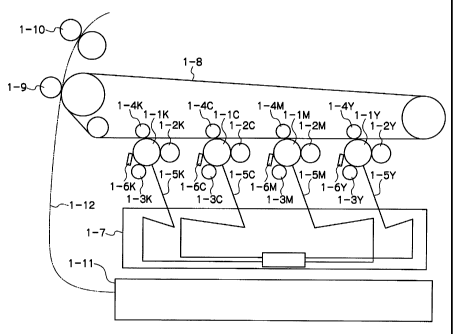
Fig. 1 is a schematic view illustrating the configuration of an embodiment of
an
image forming apparatus according to the invention. The image forming
apparatus shown
in Fig. 1 is a so-called tandem digital color printer, wherein imageforming
units for
respectively forming yellow (Y), magenta (M), cyan (C), and black (K) images
are disposed
in series with respect to the conveying direction of an image-receiving
medium. Each
imageforming unit has an electrophotographic photoreceptor (hereinafter,
referred to simply
as a "photoreceptor") supported so that it can rotate in a predetermined
direction, and a
development subunit, a charging roll, a primary transfer roll, an exposure
device and a
cleaning blade that are disposed along the traveling direction of the
peripheral surface of the
photoreceptor. A laser beam from the exposure device, ROS (Raster Output
Scanner) 1 7, is
irradiated on the charged photoreceptor. For example, the black (K) image
forming unit has
a photoreceptor 1-1K, a development subunit 1 ZK, a charging roll 1-3K, a
primary transfer
roll 1~K and a cleaning blade 1~K and causes an exposure beam 1 SK to be
irradiated on the
charged photoreceptor 1-1 K.
In such an image forming apparatus, each of the photoreceptors 1-lY, 1-1M, 1-
1C
and 1-1K has an electrically conductive substrate, and an undercoat layer and
a photosensitive
layer formed on the electrically conductive substrate, and the undercoat layer
contains metal
oxide fine particles to which an acceptor compound is added. The detail of the
configuration
of the photoreceptor will be described later.
In addition, a driving device (not shown) is connected to each photoreceptor.
The
driving device controls the rotational velocity of each photoreceptor (i.e.,
the traveling speed
of the peripheral surface of each photoreceptor), whereby the period from
charging to
CA 02501440 2005-03-18
development can be changed in each image~orming unit. Such a control function
enables
switching between plural control modes including a normal mode, a low~peed
mode, and a
high~peed mode for image formation.
For example, to form a black image, the photoreceptor 1-1K is first
electrically
charged by a charging roll 1-3K to which a voltage is applied. Then, a latent
image is
formed on the photoreceptor by exposing the photoreceptor to a laser beam 1 SK
from the
ROS (Raster Output Scanner) 1 7, and is developed with a development subunit 1
2K to form
a toner image. The toner image is transferred onto an intermediate transfer
belt under the
electric field applied by a primary transfer roll 1-~.K. The toner image is
then retransferred
onto an image-receiving medium fed from a paper tray 1-11 under the electric
field of a
secondary transfer roll 1J9 and fixed by a fixing unit 1-10, and the medium
carrying the fixed
image as a printed image is discharged from the device.
Alternatively, to form a color image in the normal mode, the yellow image
forming
unit is first driven. Thereby, a photoreceptor 1-lY is first electrically
charged by a charging
roll 1 3Y to which a voltage is applied. Then, an electrostatic latent image
is formed on the
photoreceptor by exposing the photoreceptor to a laser beam 1 SY from the ROS
1 7 and
converted into a toner image by a development subunit 1 2Y The same process is
carried
out by each of magenta (M), cyan (C), and black (K) image forming units one by
one, and the
yellow, magenta, cyan and black toner images are piled on the intermediate
transfer belt to
form a full-color image. Then, the full-color toner image is retransferred
onto an image-
receiving medium fed from the paper tray 1-11 under the electric field of the
secondary
transfer roll 1~9 and is thermally fixed by the fixing unit 1-10. The medium
carrying the
fixed image as a printed image is discharged from the device.
The rotational velocity of the photoreceptor in the normal mode is not
particularly
limited, but is preferably set so that the period from charging to development
be about 50 to
about 300 msec in each image-forming unit.
If cardboard or an OHP sheet is used as the image-receiving medium fed from
the
paper tray, it is preferable to set an image-forming mode to the low-speed
mode. In other
words, it is preferable to lengthen the period from to development and the
period for fixing in
each image~orming unit. Lengthening the period from charging to development is
attained
by slowing down the rotational velocity of the photoreceptor 1-1. The reason
why the period
for fixing is preferably lengthened is that a developer can thereby be
sufficiently fixed even
when cardboard or an OHP sheet is used. The procedure for image formation in
the low-
speed mode is the same as that in the normal mode. In addition, the rotational
velocity of the
6
CA 02501440 2005-03-18
photoreceptor (the traveling speed of the peripheral surface of each
photoreceptor) in the low-
speed mode is not particularly limited, but is preferably controlled to
satisfy the condition
represented by the following Formula (1).
T,oW >_ (1/3)T Formula (1)
In the formula, T represents the period from charging to development when an
electrophotographic process is conducted in a normal mode; and T,oW represents
that when the
electrophotographic process is carried out in a low~peed mode.
When a monochromic image (black and white image) is output, the black (K)
image-
forming unit is driven. Thereby, the photoreceptor 1-1K is first electrically
charged by the
charging roll 1 3K to which a voltage is applied. An electrostatic latent
image is formed on
the photoreceptor by exposing the photoreceptor to a laser beam 1 SK from the
ROS 1 7 and
is developed by the development subunit 1 2K to form a toner image. Then, the
toner image
is transferred onto the intermediate transfer belt 1-8 under the electric
field of the primary
transfer roll 1~K. Further, the toner image is retransferred onto an image-
receiving medium
fed from the paper tray 1-11 under the electric field of the secondary
transfer roll 1-9; the
resulting image is thermally fixed on the image-receiving medium with the
fixing unit 1-10;
and the medium carrying the fixed image as a printed image is discharged from
the device.
For formation of such monochromic images, the image-forming mode is set to a
high~peed
mode, thus accelerating the rotational velocity of the photoreceptor 1-1K and
shortening the
period from charge to development. The rotational velocity of the
photoreceptor in the high-
speed mode (the traveling speed of the peripheral surface of the
photoreceptor) is not
particularly limited, but is preferably controlled to satisfy the condition
represented by the
following Formula (2).
Th;gh <_ 3T (2) Formula (2)
In the formula, T represents the period from charging to development when an
electrophotographic process is carried out in a normal mode; and T~;gh
represents that when the
electrophotographic process is carried out in a high~peed mode.
As described above, presence of metal oxide fine particle to which an acceptor
compound is applied in the undercoat layer of each of the photoreceptors 1-1
Y, 1-1 M, 1-1 C
and 1-1K of the tandem color image~orming apparatus sufficiently improves the
electrophotographic properties of each of the photoreceptors and loosens
conditions of use
thereof. Accordingly, it becomes possible to su~ciently suppress generation of
fogging and
black spots on the output image and generation of image memory, even when the
period from
charging to development is altered by switching between the normal mode, high-
speed mode,
7
CA 02501440 2005-03-18
and low~speed mode.
Each of the units of the image~orming apparatus according to the invention
will be
described below.
First, the configuration of the photoreceptor will be described.
Fig. 2 is a schematic cross-sectional view illustrating the configuration of
an
embodiment of the electrophotographic photoreceptor of the image forming
apparatus
according to the invention. The electrophotographic photoreceptor 1-1 has a
laminated
structure wherein an undercoat layer 2, an intermediate layer 4, a
photosensitive layer 3 and a
overcoat layer 5 are laid in that order on an electrically conductive
substrate 7. The
electrophotographic photoreceptor 1-1 shown in Fig. 2 is one with layers
having different
functions, and the photorsensitive layer 3 has a charge generating layer 31
and a charge
transport layer 32.
Examples of the electrically conductive substrate 7 include drums made of a
metal
such as aluminum, copper, iron, stainless steel, zinc, or nickel; those in
which a metal such as
aluminum, copper, gold, silver, platinum, palladium, titanium, nickel~hromium,
stainless
steel, or indium, or an electrically conductive metal compound such as indium
oxide or tin
oxide is deposited on a substrate made of paper, plastic, or glass; those in
which a metal foil is
laminated on the above-described substrate; those in which the above~lescribed
substrate has
been subjected to electrically conductive treatment by applying a dispersion
in which carbon
black, indium oxide, tin oxide, antimony oxide powder, metal powder or copper
iodide is
dispersed in a binder resin thereto.
The shape of the electrically conductive substrate 7 is not restricted to the
drum
shape, and may be a sheet-dike shape or a plate-like shape. When the
electrically conductive
substrate 7 is a metal pipe, the surface of the pipe may be bare, or may be
subjected to such
treatment as mirror~urface grinding, etching, anodic oxidation, rough
grinding, centerless
grinding, sand blasting and/or wet honing.
The undercoat layer 2 contains metal oxide fine particles to which an acceptor
compound is added.
Any compound may be used as the acceptor compound, as long as it has desired
properties. However, the acceptor compound preferably has a quinone group.
Furthermore,
the acceptor compound more preferably has an anthraquinone structure. Such an
acceptor
compound is preferably anthraquinone, a hydroxyanthraquinone compound, an
aminoanthraquinone compound, an aminohydroxyanthraquinone compound, and/or a
derivative thereof. Specific examples thereof include anthraquinone, alizarin,
quinizarin,
CA 02501440 2005-03-18
anthrarufin and purpurin.
The content of the acceptor compound added is set such that desired properties
can
be obtained. It is preferably about 0.01 to about 20 weight % with respect to
the metal oxide,
and more preferably about 0.05 to about 10 weight % with respect to the metal
oxide. An
undercoat layer 2 containing the acceptor compound in an amount of less than
0.01 weight %
does not have a sufficient accepting capacity to improve prevention of charge
accumulation
therein, more easily leading to deterioration in maintaining property of the
undercoat layer,
for example, an increase in residual electric potential during repeated use.
Alternatively, an
undercoat layer 2 containing the acceptor compound in an amount of more than
20 weight %
has disadvantages in that the metal oxide particles often undesirably
aggregate, and
consequently the metal oxide cannot form desired electrically conductive paths
in the
undercoat layer 2 during formation of the undercoat layer 2, more easily
leading to
deterioration in maintaining property of the under coat layer, for example, an
increase in
residual electric potential during repeated use, and triggering image quality
defects of black
spots.
The acceptor compound can be uniformly added to the metal oxide fme particles,
for
example, by dripping a solution in which the acceptor compound is dissolved in
an organic
solvent or by spraying the solution together with dry air or a nitrogen gas on
the metal oxide
fine particles, which are being agitated with a high~hearing force mixer. The
addition or
spraying of the acceptor compound solution is preferably carried out at a
temperature equal to
or lower than the boiling point of the solvent. When the spraying is carried
out at a
temperature of higher than the boiling point of the solvent, the solvent
evaporates before
uniform agitating of the solution and the acceptor compound particles locally
aggregate and
thereby uniform processing cannot be conducted. After the addition or
spraying, the metal
oxide fine particles may be dried at a temperature equal to or higher than the
boiling point of
the solvent. Alternatively, the acceptor compound is added to the metal oxide
fme particles
by uniformly adding the acceptor compound solution to the metal oxide fme
particles
dispersed in a solvent with an agitator, an ultrasonicator, a sand mill, an
attritor or a ball mill,
agitating the resultant mixture under reflux or at a temperature equal to or
lower than the
boiling point of the organic solvent, and removing the solvent. The solvent is
usually
removed by filtration, distillation, or heat drying.
The powder resistance (volume resistivity) of the metal oxide fme particles to
which
the acceptor compound is to be added should be about 102 to about 10" S2cm.
This is
because the undercoat layer 2 should have a suitable resistance to acquire
leak resistance.
9
CA 02501440 2005-03-18
Metal oxide fine particles having a resistance lower than the lower limit of
the above range
may not provide sufficient leak resistance, while those having a resistance
higher than the
upper limit of the range may cause an increase in residual electric potential.
The metal oxide fine particles are preferably titanium oxide, zinc oxide, tin
oxide
and/or zirconium oxide fine particles having a resistance in the above range.
The metal
oxide fme particles are more preferably zinc oxide fine particles. Two or more
kinds of
metal oxide fme particles subjected to different surface treatments or having
different
diameters may be used as a mixture.
In addition, the metal oxide fine particles preferably have a specific surface
area of
mz/g or more. Metal oxide fine particles having a specific surface area of
lower than 10
mz/g easily cause deterioration in electrostatic properties, making it
difficult to obtain good
electrophotographic properties.
The metal oxide fine particles may be subjected to surface treatment before
addition
of the acceptor compound. Any known surface treating agent may be used, as
long as it
provides desired properties. Examples thereof include coupling agents such as
silane
coupling agents, titanate coupling agents, and aluminum coupling agents; and
surface-active
agents. Use of a silane coupling agent is particularly favorable, since it
provides good
electrophotographic properties. Typical examples of the silane coupling agent
include, but
are not limited to, vinyltrimethoxysilane, y~nethacryloxypropyl-tris((3-
methoxyethoxy)silane,
/3-(3,4-~poxycyclohexyl)ethyltrimethoxysilane, y-
glycidoxypropyltrimethoxysilane,
vinyltriacetoxysilane, y-inercaptopropyltrimethoxysilane,
y~minopropyltriethoxysilane, N~i-
(aminoethyl)-y~minopropyltrimethoxysilane, N-(3~aminoethyl)jy-
aminopropylmethylmethoxysilane, N,N-bis((3-hydroxyethyl)Jy-
aminopropyltriethoxysilane,
and y~hloropropyltrimethoxysilane. In addition, two or more of these coupling
agents may
be used as a mixture.
Further, an amino group-containing silane coupling agent is preferably used,
since it
can provide the undercoat layer 2 with a good blocking property.
The amino group-containing silane coupling agent is not particularly limited,
as long
as it provides the electrophotographic photoreceptor with good properties.
Typical examples
thereof include, but are not limited to, y-aminopropyltriethoxysilane, N-~3-
(aminoethyl)~y-
aminopropyltrimethoxysilane, N-(3-
{aminoethyl)~y~minopropylmethylmethoxysilane, and
N,N-bis((3-hydroxyethyl)jy-aminopropyltriethoxysilane.
Two silane coupling agents may be used together. Examples of the silane
coupling
CA 02501440 2005-03-18
agent that may be used together with the amino group-containing silane
coupling agent
include, but are not limited to, vinyltrimethoxysilane, y-~nethacryloxypropyl-
tris((3-
methoxyethoxy)silane, (3-{3,4~poxycyclohexyl)ethyltrimethoxysilane, y-
glycidoxypropyltrimethoxysilane, vinyltriacetoxysilane, ~y-
mercaptopropyltrimethoxysilane, y-
aminopropyltriethoxysilane, N-j3~aminoethyl)fy-aminopropyltrimethoxysilane,
N~i-
(aminoethyl)jy-aminopropylmethylmethoxysilane, N,N-bis((3-hydroxyethyl)jy-
aminopropyltriethoxysilane, and y-chloropropyltrimethoxysilane.
Any known method may be used as a surface treatment method, and specifically
dry
and wet methods can be used.
When dry surface treatment is carried out, the metal oxide fine particles are
uniformly processed by adding a silane coupling agent directly or spraying a
solution, in
which the silane coupling agent is dissolved in an organic solvent, together
with dry air or
nitrogen gas stream onto the metal oxide particles, which are being agitated
with a high-
shearing force mixer. The addition or spraying is preferably carried out at a
temperature
equal to or lower than the boiling point of the solvent. When spraying is
carried out at a
temperature of higher than the boiling point of the solvent, the solvent
evaporates before
uniform agitating of the silane coupling agent and the silane coupling agent
becomes localized,
making it difficult to conduct uniform processing. The metal oxide fine
particle may be
baked at a temperature of 100°C or more after the addition or spraying.
The baking
temperature and time may be set such that desirable electrophotographic
properties can be
obtained.
In wet methods, the metal oxide fine particles are processed uniformly by
dispersing
the metal oxide fine particles in a solvent with an agitator, an
ultrasonicator, a sand mill, an
attritor, or a ball mill, adding a silane coupling agent solution to the
particles, agitating the
resulting mixture, and removing the solvent. The solvent is usually removed by
filtration or
distillation. The metal oxide fine particles may be baked at a temperature of
100°C or more.
The baking temperature and time may be set such that desirable
electrophotographic
properties can be obtained. In the wet methods, moisture contained in the
metal oxide fine
particles may be removed before the addition of a surface treating agent, for
example, by
heating and agitating the particles in a solvent used in surface treatment or
by azeotropic
distillation of water and the solvent.
The amount of the silane coupling agent with respect to that of the metal
oxide fine
particles in the undercoat layer 2 may be freely selected, as long as it is
proper for providing
11
CA 02501440 2005-03-18
desired electrophotographic properties.
The binder resin for use in the undercoat layer 2 is not particularly limited,
as long as
it forms a good film and provides the film with desired properties. The binder
resin can be a
known polymer resin compound. Examples thereof include acetal resins such as
polyvinyl
butyral, polyvinyl alcohol resins, casein, polyamide resins, cellulose resins,
gelatin,
polyurethane resins, polyester resins, methacrylic resins, acrylic resins,
polyvinyl chloride
resins, polyvinyl acetate resins, vinyl chloride vinyl acetate-inaleic
anhydride resins, silicone
resins, silicone~lkyd resins, phenol resins, phenol~ormaldehyde resins,
melamine resins, and
urethane resins. The binder resin can also be a charge transport resin having
a charge
transport group or an electrically conductive resin such as polyaniline. Among
them, a resin
insoluble in coating solutions for layers on or above the undercoat layer is
preferable as the
binder resin. Typical examples thereof include phenol resins, phenol-
formaldehyde resins,
melamine resins, urethane resins, and epoxy resins.
The ratio of the metal oxide fine particles to the binder resin in the coating
solution
for forming an undercoat layer 2 may be freely selected, as long as an
electrophotographic
photoreceptor with desired properties can be obtained.
Various additives may be added to the coating solution for forming an
undercoat
layer 2 in order to improve electrical properties, environmental stability,
and/or image quality.
Examples of such additives include electron transport materials including
quinone
compounds such as chloranil and bromoanil, tetracyanoquinodimethane compounds,
fluorenone compounds such as 2,4,7-trinitrofluorenone and 2,4,5,7-
tetranitro~9~luorenone,
oxadiazole compounds such as 2-{4-biphenyl) 5-{4-t-butylphenyl)-
1,3,4~xadiazole, 2,5-
bis(4~aphthyl)-1,3,4~xadiazole, and 2,5-
bis(4~iiethylaminophenyl)1,3,4oxadiazole,
xanthone compounds, thiophene compounds, and diphenoquinone compounds such as
3,3',5,5'-~etra~-butyldiphenoquinone; electron transport pigments such as
polycyclic
condensates and azo pigments; zirconium chelate compounds, titanium chelate
compounds,
aluminum chelate compounds, titanium alkoxide compounds, organic titanium
compounds,
and silane coupling agents. A silane coupling agent is used in surface
treatment of zinc
oxide, but may be added to the coating solution as an additive. Typical
examples of the
silane coupling agent include vinyltrimethoxysilane, y-
methacryloxypropyl~ris((3-
methoxyethoxy)silane, (3-{3,4-epoxycyclohexyl)ethyltrimethoxysilane, y-
glycidoxypropyltrimethoxysilane, vinyltriacetoxysilane, y-
mercaptopropyltrimethoxysilane, y-
aminopropyltriethoxylsilane, N-i3-(aminoethyl)-=y~minopropyltrimethoxysilane,
N-~3-
12
CA 02501440 2005-03-18
(aminoethyl)jy-aminopropylmethylmethoxysilane, N,Nfiis(~i-hydroxyethyl)-~y-
aminopropyltriethoxysilane, and y-chloropropyltrimethoxysilane. Examples of
the
zirconium chelate compound include zirconium butoxide, ethyl zirconium
acetoacetate,
zirconium triethanolamine, acetylacetonatozirconium butoxide, ethyl zirconium
butoxide
acetoacetate, zirconium acetate, zirconium oxalate, zirconium lactate,
zirconium phosphonate,
zirconium octanate, zirconium naphthenate, zirconium laurate, zirconium
stearate, zirconium
isostearate, methacrylatozirconium butoxide, stearatozirconium butoxide and
isostearatozirconium butoxide.
Examples of the titanium chelate compound include tetraisopropyl titanate,
tetra-n-
butyl titanate, butyl titanate dimer, tetra(2-ethylhexyl) titanate, titanium
acetylacetonate,
polytitanium acetylacetonate, titanium octyleneglycolate, titanium lactate
ammonium salt,
titanium lactate, titanium lactate ethylester, titanium triethanol aminate,
and
polyhydroxytitanium stearate.
Examples of the aluminum chelate compound include aluminum isopropylate,
monobutoxyaluminum diisopropylate, aluminum butylate,
diethylacetoacetatoaluminum
diisopropylate, and aluminum tris(ethylacetoacetate).
One of these compound may be used alone or two or more of them can be used as
a
mixture or polycondensate.
The solvent used in the coating solution for forming an undercoat layer may be
selected freely from known organic solvents, such as alcohols, aromatic
compounds,
halogenated hydrocarbons, ketones, ketone alcohols, ethers, and esters. More
specifically,
an ordinary organic solvent such as methanol, ethanol, n~ropanol, iso-
propanol, n-butanol,
benzyl alcohol, methylcellusolve, ethylcellusolve, acetone, methyl ethyl
ketone,
cyclohexanone, methyl acetate, ethyl acetate, n-butyl acetate, dioxane,
tetrahydrofuran,
methylene chloride, chloroform, chlorobenzene, and toluene may be used as
such.
One of these solvents for dispersion may be used alone or two or more of them
can
be used as a mixture. In a case of a mixture of two or more solvents, any
mixed solvent can
be used, as long as it can dissolve the binder resin.
Known methods using a roll mill, a ball mill, a vibration ball mill, an
attritor, a sand
mill, a colloid mill, and a paint shaker may be used to disperse the metal
oxide fine particles.
In addition, application methods for use in forming the undercoat layer 2
include ordinary
methods such as blade coating, wire bar coating, spray coating, dip coating,
bead coating, air
knife coating, and curtain coating methods.
The undercoat layer 2 is formed on the electrically conductive substrate 7
using the
13
CA 02501440 2005-03-18
coating solution for forming an undercoat layer 2 thus obtained.
The undercoat layer 2 preferably has a Vickers' strength of 35 or more. In
addition,
the undercoat layer 2 preferably has a thickness of 15 pm or more, and more
preferably a
thickness of about 20 to about 50 pm.
An undercoat layer 2 having a thickness of less than 15 p,m has a drawback of
not
providing sufficient leak resistance, while an undercoat layer having a
thickness of more than
50 p,m has a drawback of leading to image density abnormalities due to
residual electric
potential easily remaining during long~erm use.
For prevention of Moire images, the surface roughness of the undercoat layer 2
is
adjusted to about 1/4n (n is the refractive index of an upper layer) to about
1/2 of the
wavelength ~, of exposure laser beam used. Resin particles may be contained in
the
undercoat layer for adjustment of the surface roughness. The resin particles
are, for example,
silicone resin particles and/or cross~inked PMMA resin particles.
In addition, the undercoat layer 2 may be polished for adjustment of the
surface
roughness, and examples of polishing methods include buffing, sand blasting,
wet honing, and
grinding treatment.
An intermediate layer 4 may be formed between the undercoat layer 2 and the
photosensitive layer 3 for improvements in electrical properties, image
quality, image quality
endurance, and adhesiveness between the undercoat layer and the photosensitive
layer.
The materials of the intermediate layer 4 include polymer resin compounds, for
example, acetal resins such as polyvinyl butyral, polyvinyl alcohol resins,
casein, polyamide
resins, cellulose resins, gelatin, polyurethane resins, polyester resins,
methacrylic resins,
acrylic resins, polyvinyl chloride resins, polyvinyl acetate resins, vinyl
chloride~inyl acetate-
maleic anhydride resins, silicone resins, silicone- alkyd resins,
phenol~ormaldehyde resins,
melamine resins; and organic metal compounds containing zirconium, titanium,
aluminum,
manganese, and/or silicon atoms. One of these compounds may be used alone or
two or
more of them can be used as a mixture or polycondensate. Among them, a
zirconium- or a
silicon-containing organic metal compound is superior in various properties,
since it has low
residual electric potential and exhibits small fluctuations in electric
potential caused by the
environment and in electric potential caused by repeated use.
Examples of the silicon compound include vinyltrimethoxysilane, y-
methacryloxypropyl~ris(~i~nethoxyethoxy)silane, ~3-(3,4-
epoxycyclohexyl)ethyltrimethoxysilane, y-glycidoxypropyltrimethoxysilane,
14
CA 02501440 2005-03-18
vinyltriacetoxysilane, y~nercaptopropyltrimethoxysilane,
y~minopropyltriethoxylsilane, N~3-
(aminoethyl)-~y~minopropyltrimethoxysilane, N~3-(aminoethyl)jy-
aminopropylmethylmethoxysilane, N,N-bis((3-hydroxyethyl)-
~y~minopropyltriethoxylsilane,
and y-chloropropyltrimethoxysilane. The silicon compound is particularly
favorably a silane
coupling agent such as vinyltriethoxylsilane, vinyltris(2-
methoxyethoxy)silane, 3-
methacryloxypropyltrimethoxysilane, 3~lycidoxypropyltrimethoxysilane, 2~3,4-
epoxycyclohexyl)ethyltrimethoxysilane, N 2-(aminoethyl)3-
atninopropyltrimethoxysilane, N-
2-(aminoethyl) 3-~minopropylmethyldimethoxysilane, 3-
aminopropyltriethoxylsilane, N-
phenyl-3-aminopropyltrimethoxysilane, 3~nercaptopropyltrimethoxysilane, and 3-
chloropropyltrimethoxysilane.
Examples of the organic zirconium compound include zirconium butoxide, ethyl
zirconium acetoacetate, zirconium triethanolamine, acetylacetonatozirconium
butoxide, ethyl
zirconium butoxide acetoacetate, zirconium acetate, zirconium oxalate,
zirconium lactate,
zirconium phosphonate, zirconium octanate, zirconium naphthenate, zirconium
laurate,
zirconium stearate, zirconium isostearate, methacrylatozirconium butoxide,
stearatozirconium
butoxide and isostearatozirconium butoxide.
Examples of the organic titanium compound include tetraisopropyl titanate,
tetra-n-
butyl titanate, butyl titanate dimer, tetra(2-ethylhexyl) titanate, titanium
acetylacetonate,
polytitanium acetylacetonate, titanium octyleneglycolate, titanium lactate
ammonium salt,
titanium lactate, titanium lactate ethylester, titanium triethanol aminate,
and
polyhydroxytitanium stearate.
Examples of the organic aluminum compound include aluminum isopropylate,
monobutoxyaluminum diisopropylate, aluminum butylate,
diethylacetoacetatoaluminum
diisopropylate, and aluminum tris(ethylacetoacetate).
The intermediate layer 4 not only improves the coating properties of layers on
or
above the intermediate layer but also serves as an electrical blocking layer.
However, a too
thick intermediate layer becomes more electrically resistant, leading to a
decrease in
sensitivity of the photoreceptor and an increase in electric potential due to
repeated use.
Accordingly, if formed, the intermediate layer 4 has a thickness in the range
of about 0.1 to
about 5 pm.
The charge generating layer 31 in the photosensitive layer 3 is formed by
vacuum-
depositing a charge generating material or by coating a dispersion containing
such a material,
a binder resin and an organic solvent to the undercoat or intermediate layer,
or a charge
CA 02501440 2005-03-18
transport layer described later.
If formed by dispersion and coating, the charge generating layer 31 is formed
by
dispersing a charge generating material together, a binder resin, and
additives in an organic
solvent, and coating the dispersion thus obtained.
Any known charge generating substance may be used as the charge generating
material in the invention. Examples of those for infrared light include
phthalocyanine
pigments, squarylium compounds, bisazo compounds, trisazo pigments, perylene
compounds,
and dithioketopyrrolopyrrole. Examples of those for visible Iight include
condensed
polycyclic pigments, bisazo compounds, perylene compounds, trigonal selenium
compounds,
and dye~ensitized zinc oxide fine particles. Charge generating materials
providing excellent
properties and therefore particularly favorably used are phthalocyanine
pigments and azo
pigments. Use of a phthalocyanine pigment enables production of an
electrophotographic
photoreceptor having particularly superior sensitivity and stability during
repeated use.
Phthalocyanine pigments and azo pigments generally have several crystal forms.
A
phthalocyanine or azo pigment having any of these crystal forms may be used,
as long as it
can provide desirable electrophotographic properties. Typical examples of the
phthalocyanine pigment include chlorogallium phthalocyanine, dichlorotin
phthalocyanine,
hydroxygallium phthalocyanine, metal~ree phthalocyanine,
oxytitanylphthalocyanine, and
chloroindium phthalocyanine.
The phthalocyanine pigment crystals may be prepared by mechanical, dry
pulverization of a phthalocyanine pigment prepared in accordance with a known
method with
an automatic mortar, a planetary mill, a vibration mill, a CF mill, a roller
mill, a sand mill
and/or a kneader, and optionally by wet pulverization of the crystal obtained
by the dry
pulverization in a solvent with a ball mill, a mortar, a sand mill and/or a
kneader.
Examples of the solvent used in the process described above include aromatic
compounds (e.g., toluene, and chlorobenzene), amides (e.g., dimethylformamide,
and N-
methylpyrrolidone), aliphatic alcohols (e.g, methanol, ethanol, and butanol),
aliphatic
polyhydric alcohols (e.g., ethylene glycol, glycerol, and polyethylene
glycol), aromatic
alcohols (e.g., benzyl alcohol, and phenethyl alcohol), esters (e.g., acetic
acid esters, including
butyl acetate), ketones (e.g., acetone, and methyl ethyl ketone),
dimethylsulfoxide, and ethers
(e.g., diethyl ether, and tetrahydrofuran), and mixtures thereof, and mixtures
each including at
least one of these organic solvents and water. The amount of the solvent is in
the range of
about 1 to about 200 parts, and preferably about 10 to about 100 parts by
weight with respect
to the pigment crystals. The processing temperature is in the range of about
20°C to the
16
CA 02501440 2005-03-18
boiling point of the solvent and more preferably in the range of about -10 to
about 60°C. A
grinding aid such as sodium chloride and/or Glauber's salt may be additionally
used during
pulverization. The amount of the grinding aid is about 0.5 to about 20 times,
and preferably
about 1 to about 10 times as much as that of the pigment.
The crystalline state of phthalocyanine pigment crystal prepared in accordance
with a
known method can be controlled with acid pasting or a combination of the acid
pasting and
the dry or wet pulverization described above. An acid for use in the acid
pasting is
preferably sulfuric acid at a concentration of about 70 to 100%, and
preferably of about 95 to
100% . The solubilization temperature is in the range of about 20 to about
100°C and
preferably in the range of about -10 to about 60°C. The amount of conc.
sulfuric acid is
about 1 to about 100 times, and preferably about 3 to about 50 times as much
as that of
phthalocyanine pigment crystal. Water or a mixture of water and an organic
solvent is used
in an arbitrary amount as a solvent for precipitating the crystal. The
precipitation
temperature is not particularly limited, but the pigment crystals are
preferably cooled, for
example, with ice for prevention of heat generation.
Hydroxygallium phthalocyanine, which is most preferably used among them, has
diffraction peaks at Bragg angles (28 ~ 0.2°) of 7.5°,
9.9°, 12.5°, 16.3°, 18.6°, 25.1°, and
28.3° as determined by using X-iay having Cuka characteristics. I-type
hydroxygallium
phthalocyanine used as a raw material in preparation of hydroxygallium
phthalocyanine can
be prepared in accordance with any known method. An example thereof is shown
below.
First, crude gallium phthalocyanine is produced, for example, by a method of
reacting o~hthalodinitrile or 1,3-diiminoisoindoline with gallium trichloride
in a
predetermined solvent (I-type chlorogallium phthalocyanine method); or a
method of
preparing phthalocyanine dimer by heating and allowing o~hthalodinitrile, an
alkoxy gallium,
and ethylene glycol to react in a predetermined solvent (phthalocyanine dimer
method).
Examples of the solvent preferably used in the above reactions include
inactive, high-boiling
point solvents such as a-chloronaphthalene, (3-chloronaphthalene, a-
methylnaphthalene,
methoxynaphthalene, dimethylaminoethanol, diphenylethane, ethylene glycol,
dialkylethers,
quinoline, sulfolane, dichlorobenzene, dimethylformamide, dimethylsulfoxide,
and
dimethylsulfoamide.
The crude gallium phthalocyanine thus obtained is then subjected to acid
pasting
treatment, which converts the crude gallium phthalocyanine into fme particles
of I-type
hydroxygallium phthalocyanine pigment. Specifically, the acid pasting
treatment is
17
CA 02501440 2005-03-18
recrystallization of gallium phthalocyanine, for example, by pouring a
solution in which the
crude gallium phthalocyanine is dissolved in an acid such as sulfric acid into
an aqueous
alkaline solution, water or ice water, or by adding an acid salt of the crude
gallium
phthalocyanine such as a sulfate salt to the aqueous alkaline solution, water
or ice water.
The acid used in the acid pasting treatment is preferably sulfuric acid, and
the sulfuric acid
preferably has a concentration of about 70 to 100% (more preferably about 9S
to 100%).
The hydroxygallium phthalocyanine usable in the invention can be obtained by
pulverizing the I-type hydroxygallium phthalocyanine pigment obtained by the
acid pasting
treatment in a solvent and thus altering the crystal form of the pigment. This
wet
pulverization treatment is preferably carried out with a pulverizes employing
spherical media
having an outer diameter of about 0.1 to about 3.0 mm, more preferably
employing those
having an outer diameter of about 0.2 to about 2.5 mm. If the outer diameter
of the media is
greater than 3.0 mm, pulverization efficiency deteriorates and the
hydroxygallium
phthalocyanine particles do not become smaller and easily aggregate.
Alternatively, if it is
less than 0.1 mm, it becomes difficult to separate hydroxygallium
phthalocyanine powder
from the media. In addition, when the media have a shape other than sphere
such as a
cylindrical or irregular shape, pulverization efficiency lowers, and the media
easily wear due
to pulverization, and fractured powders occurring from wear of the media
serves as impurities
and accelerate deterioration of the properties of hydroxygallium
phthalocyanine.
Any material may be used for the media, but the media is preferably made of
what
never or hardly causes image quality defects even when introduced into the
pigment, such as
glass, zirconia, alumina, or agate.
Any material rnay be used for the container, but the container is preferably
made of
what never or hardly causes image quality defects even when introduced into
the pigment,
such as glass, zirconia, alumina, agate, polypropylene, TEFLON (registered
trade name),
and/or polyphenylene sulfide. Further, the internal surface of a container
made of a metal
such as iron or stainless steel may be lined with glass, polypropylene, TEFLON
(registered
trade name) and/or polyphenylene sulfide.
The amount of the media used may depend on the type of a device used, but is
generally 50 parts by weight or more, and preferably about 55 to about 100
parts by weight
with respect to 1 part by weight of I-type hydroxygallium phthalocyanine
pigment. When
the weight of the media is constant, a decrease in the outer diameter of the
media leads to an
increase in the density of the media in the device, an increase in the
viscosity of the mixture
solution and a change in pulverization efficiency. Therefore, it is preferable
to conduct wet
18
CA 02501440 2005-03-18
pulverization at a controlled, optimal mixing rate of the amounts of the media
and the solvents
used, as the medium outer diameter is reduced.
The temperature of the wet pulverization treatment is generally in the range
of about
0 to about 100°C, preferably in the range of about 5 to about
80°C, and more preferably in the
range of about 10 to about 50°C. Wet pulverization at a lower
temperature results in
slowdown of crystal conversion, while that at an excessively high temperature
results in an
increase in the solubility of hydroxygallium phthalocyanine and crystal
growth, making it
difficult to produce fine particles.
Examples of the solvent for use in the wet pulverization treatment include
amides
such as N,N-dimethylformamide, N,N-dimethylacetamide, and N~nethylpyrrolidone;
esters
such as ethyl acetate, n-butyl acetate, and iso-amyl acetate; ketones such as
acetone, methyl
ethyl ketone, and methyl iso-butyl ketone; and dimethylsulfoxide. The amount
of the
solvent used is usually about 1 to about 200 parts by weight, and preferably
about 1 to about
100 parts by weight with respect to 1 part by weight of the hydroxygallium
phthalocyanine
pigment.
Examples of an apparatus used in the wet pulverization treatment include mills
employing a dispersion medium such as a vibration mill, an automatic mortar, a
sand mill, a
dyno mill, a cobalt mill, an attritor, a planetary ball mill, and a ball mill.
The progress speed of the crystal conversion is significantly influenced by
the scale,
agitating speed and the material of the media of the wet pulverization
process. The process
is continued until the original crystal form of hydroxygallium phthalocyanine
is converted to
the desired crystal form thereof. At this time, the crystal-converting state
of hydroxygallium
phthalocyanine is monitored by measuring the light absorption of the solution,
which is being
subjected to wet pulverization. The process is continued until the absorption
peak of the
hydroxygallium phthalocyanine which absorption peak is maximum in the
spectroscopic
absorption spectrum of 600 to 900 nm becomes within the range of 810 to 839
nm.
Generally, the duration of the wet pulverization treatment is generally in the
range of about 5
to about 500 hours and preferably in the range of about 7 to about 300 hours.
A treatment
period of shorter than 5 hours may result in incomplete crystal conversion,
leading to
deterioration in electrophotographic properties, in particular, in
sensitivity. A treatment
period of longer than 500 hours may cause decreases in sensitivity and
productivity, and
contamination of the pigment with fractured powder of the medium due to the
influence of
pulverization stress. Wet pulverization continued for the period of time
described above
allows the hydroxygallium phthalocyanine particles to be uniformly pulverized
and converted
19
CA 02501440 2005-03-18
into fine particles.
The binder resin for use in the charge generating layer 31 may be selected
from a
wide variety of insulating resins or from organic photoconductive polymer such
as poly-N-
vinylcarbazole, polyvinylanthracene, polyvinylpyrene, and polysilane. Typical
examples of
the binder resin include, but are not limited to, polyvinylacetal resins,
polyarylate resins (e.g.,
poly~ondensed polymers made from bisphenol A and phthalic acid), polycarbonate
resins,
polyester resins, phenoxy resins, vinyl chloridewinyl acetate copolymers,
polyamide resins,
acrylic resins, polyacrylamide resins, polyvinylpyridine resins, cellulose
resins, urethane
resins, epoxy resins, casein, polyvinyl alcohol resins and
polyvinylpyrrolidone resins. One
of these binder resins may be used alone, or two or more of them can be used
as a mixture.
Among them, the binder resin is particularly preferably a polyvinyl acetal
resin.
The blending ratio (weight ratio) of the charge generating material to the
binder resin
in the coating solution for forming a charge generating layer is preferably in
the range of 10:1
to 1:10. The solvent used in the coating solution may be selected arbitrarily
from known
organic solvents such as alcohols, aromatic compounds, halogenated
hydrocarbons, ketones,
ketone alcohols, ethers, and esters. Specific examples thereof include
ordinary organic
solvents such as methanol, ethanol, n~ropanol, iso~ropanol, n-~utanol, benzyl
alcohol,
methylcellusolve, ethylcellusolve, acetone, methyl ethyl ketone,
cyclohexanone, methyl
acetate, ethyl acetate, n-butyl acetate, dioxane, tetrahydrofuran, methylene
chloride,
chloroform, chlorobenzene, and toluene.
One of these solvents for use in dispersion may be used alone, or two or more
of
them can be used as a mixture. When two or more solvents are mixed, these are
selected
such that the mixed solvent can dissolve the binder resin.
Examples of a dispersion method include methods using a roll mill, a ball
mill, a
vibration ball mill, an attritor, a sand mill, a colloid mill and a paint
shaker. A method for
applying a coating solution for a charge generating layer to the undercoat or
intermediate
layer can be any common method including blade coating, wire bar coating,
spray coating, dip
coating, bead coating, air knife coating and curtain coating methods.
Further, it is effective to adjust the size of dispersed particles to a value
in the rage of
of 0.5 pm or less, preferably 0.3 pm or less, and more preferably 0.15 p.m or
less in
improving sensitivity and stability.
The charge generating substance may be surface-treated for improvement in the
stability of electrical properties and prevention of image quality defects.
Such surface
treatment improves dispersing property of the charge generating substance and
coatability of
CA 02501440 2005-03-18
the coating solution for a charge generating layer, enables easy and secure
production of a
smooth charge generating layer 31 in which the substance is uniformly
dispersed,
consequently suppresses image quality defects such as fogging and ghosts, and
thus improves
image quality endurance. It also improves the storage life of the coating
solution for a
charge generating layer and thus is effective in extending the pot life
thereof, enabling cost
reduction of the photoreceptor.
An organic metal compound or a silane coupling agent having a hydrolyzable
group
may be used as the surface-treating agent.
The organic metal compound or the silane coupling agent having a hydrolyzable
group is preferably represented by the following Formula (A):
Formula (A) Rp~VI Yq
In the formula, R represents an organic group; M represents a metal other than
an
alkali metal, or a silicon atom; Y represents a hydrolyzable group; and p and
q each are an
integer of 1 to 4 and the total of p and q is equivalent to the valence of M.
Examples of the organic group represented by R in Formula (A) include alkyl
groups
such as methyl, ethyl, propyl, butyl, and octyl groups; alkenyl groups such as
vinyl and allyl
groups; cycloalkyl groups such as a cyclohexyl group; aryl groups such as
phenyl and
naphthyl groups; alkylaryl groups such as a toluyl group; arylalkyl groups
such as benzyl and
phenylethyl group; arylalkenyl groups such as a styryl group; and heterocyclic
residues such
as fiuyl, thienyl, pyrrolidinyl, pyridyl, and imidazolyl groups. The organic
group may have
one or more substituents.
Examples of the hydrolyzable group represented by Y in Formula (A) include
ether
groups such as methoxy, ethoxy, propoxy, butvxy, cyclohexyloxy, phenoxy, and
benzyloxy
group; ester groups such as acetoxy, propionyloxy, acryloxy, methacryloxy,
benzoyloxy,
methanesulfonyloxy, benzenesulfonyloxy, and benzyloxycarbonyl groups; and
halogen atoms
such as a chlorine atom.
In Formula (A), M is not particularly limited, if it is not an alkali metal. M
is
preferably a titanium atom, an aluminum atom, a zirconium atom, or a silicon
atom.
Accordingly, organic titanium compounds, organic aluminum compounds, organic
zirconium
compounds, and silane coupling agents which are substituted with the organic
group or
hydrolyzable group described above are preferably used in the invention.
Examples of the silane coupling agent include vinyltrimethoxysilane, y-
methacryloxypropyl-tris((3-methoxyethoxy)silane, (3-(3,4-
21
CA 02501440 2005-03-18
epoxycyclohexyl)ethyltrimethoxysilane, y~lycidoxypropyltrimethoxysilane,
vinyltriacetoxysilane, y~nercaptopropyltrimethoxysilane,
y~minopropyltriethoxysilane, N-[3-
(aminoethyl)~y~minopropyltrimethoxysilane, N-~3~aminoethyl)jy-
aminopropylmethylmethoxysilane, N,N-bis(~3-hydroxyethyl)~-
aminopropyltriethoxysilane
and y~hloropropyltrimethoxysilane. Among them, the silane coupling agent is
more
preferably vinyltriethoxysilane, vinyltris(2~nethoxyethoxy)silane, 3-
methacryloxypropyltrimethoxysilane, 3-glycidoxypropyltrimethoxysilane, 2-(3,4-
epoxycyclohexyl)ethyltrimethoxysilane, N 2-(aminoethyl) 3-
aminopropyltrimethoxysilane,
N 2-{aminoethyl)-3~minopropylmethyldimethoxysilane, 3-
aminopropyltriethoxysilane, N-
phenyl 3-aminopropyltrimethoxysilane, 3-mercaptopropyltrimethoxysilane, and/or
3-
chloropropyltrimethoxysilane.
Examples of the organic zirconium compound include zirconium butoxide, ethyl
zirconium acetoacetate, zirconium triethanolamine, acetylacetonatozirconium
butoxide, ethyl
zirconium butoxide acetoacetate, zirconium acetate, zirconium oxalate,
zirconium lactate,
zirconium phosphonate, zirconium octanate, zirconium naphthenate, zirconium
laurate,
zirconium stearate, zirconium isostearate, methacrylatozirconium butoxide,
stearatozirconium
butoxide and isostearatozirconium butoxide.
Examples of the organic titanium compound include tetraisopropyl titanate,
tetra-n-
butyl titanate, butyl titanate dimer, tetra(2-ethylhexyl) titanate, titanium
acetylacetonate,
polytitanium acetylacetonate, titanium octyleneglycolate, titanium lactate
ammonium salt,
titanium lactate, titanium lactate ethyl ester, titanium triethanol aminate,
and
polyhydroxytitanium stearate. Examples of the organic aluminum compound
include
aluminum isopropylate, monobutoxyaluminum diisopropylate, aluminum butylate,
diethylacetoacetatoaluminum diisopropylate, and aluminum
tris(ethylacetoacetate).
Hydrolysates of the organic metal compounds and the silane coupling agents may
also be used. Examples of the hydrolysate include those in which Y
(hydrolyzable group)
bonding to M (a metal atom other than an alkali metal, or a silicon atom) in
the organic metal
compound represented by the formula described above and/or an hydrolyzable
group bonding
to R (organic group) has been hydrolyzed. In this case, if the organic metal
compound or the
silane coupling agent has plural hydrolyzable groups, it is unnecessary that
all the functional
groups on the compound have been hydrolyzed. In other words, a partially
hydrolyzed
product may be used in the invention. One of these organic metal compounds and
the silane
coupling agents may be used alone, or two or more of them can be used
together.
22
CA 02501440 2005-03-18
Examples of a method for coating a phthalocyanine pigment with an organic
metal
compound and/or a silane coupling agent having a hydrolyzable group
(hereinafter, referred to
simply as "organic metal compound") include a method for coating the
phthalocyanine
pigment with the agent at the time that the crystal form of the phthalocyanine
pigment is
being changed, a method for conducting the coating treatment before the
phthalocyanine
pigment is dispersed in the binder resin, a method for mixing the organic
metal compound
with the pigment in dispersing the phthalocyanine pigment in the binder resin,
and a method
for dispersing an organic metal compound in a binder resin in which the
phthalocyanine
pigment has been dispersed.
More specifically, examples of the method for conducting the coating treatment
at the
time that the crystal form of the phthalocyanine pigment is being changed
include a method
for mixing the organic metal compound with the phthalocyanine pigment whose
crystal form
has not been changed and heating the resultant mixture, a method for mixing
the organic
metal compound with the phthalocyanine pigment whose crystal form has not been
changed
and mechanically pulverizing the resultant mixture in a dry manner, and a
method for mixing
a liquid mixture in which the organic metal compound is dissolved in water or
an organic
solvent with the phthalocyanine pigment whose crystal form has not been
changed and
conducting wet~ulverization treatment.
Examples of the method for conducting the coating treatment before the
phthalocyanine pigment is dispersed in the binder resin include a method for
mixing the
organic metal compound, water or a liquid mixture of water and an organic
solvent, and the
phthalocyanine pigment and heating the resultant mixture, a method for
directly spraying the
organic metal compound on the phthalocyanine pigment, and a method for mixing
and milling
the organic metal compound and the phthalocyanine pigment.
Further, examples of the method for mixing the organic metal compound with the
pigment in dispersing the phthalocyanine pigment in the binder resin include a
method for
sequentially adding the organic metal compound, the phthalocyanine pigment,
and the binder
resin to a dispersion solvent and stirring the resultant mixture, and a method
for
simultaneously adding these components of a charge generating layer to a
solvent and mixing
the resultant.
Various additives may be added to the coating solution for a charge generating
layer
to improve electrical properties of the layer and image quality. The additives
can be known
materials. Examples thereof include electron transport materials including
quinone
compounds such as chloranil, bromoanil, and anthraquinone,
tetracyanoquinodimethane
23
CA 02501440 2005-03-18
compounds, fluorenone compounds such as 2,4,7~rinitrofluorenone and
2,4,5,7~etranitro~9-
fluorenone, oxadiazole compounds such as 2-(4~fiiphenyl) 5-(4-t-butylphenyl)-
1,3,4-
oxadiazole, 2,5-bis(4~aphthyl)-1,3,4-oxadiazole, and 2,Sfiis(4-
diethylaminophenyl)-1,3,4-
oxadiazole, xanthone compounds, thiophene compounds, diphenoquinone compounds
such as
3,3',5,5'~etra-t-butyl diphenoquinone; electron transport pigments such as
polycyclic
condensed compounds, and azo pigments; zirconium chelate compounds, titanium
chelate
compounds, aluminum chelate compounds, titanium alkoxide compounds, organic
titanium
compounds, and silane coupling agents.
Examples of the silane coupling agent include vinyltrimethoxysilane, y-
methacryloxypropyl-tris(~3-~nethoxyethoxy)silane, (3-~3,4-
epoxycyclohexyl)ethyltrimethoxysilane, y-glycidoxypropyltrimethoxysilane,
vinyltriacetoxysilane, y-mercaptopropyltrimethoxysilane, Y-
aminopropyltriethoxysilane, N~3-
(aminoethyl)~y~minopropyltrimethoxysilane, N-~3~aminoethyl)jy-
aminopropylmethylmethoxysilane, N,N-bis((3-hydroxyethyl)-~y-
aminopropyltriethoxysilane
and y-chloropropyltrimethoxysilane.
Examples of the zirconium chelate compound include zirconium butoxide, ethyl
zirconium acetoacetate, zirconium triethanolamine, acetylacetonatozirconium
butoxide, ethyl
zirconium butoxide acetoacetate, zirconium acetate, zirconium oxalate,
zirconium lactate,
zirconium phosphonate, zirconium octanate, zirconium naphthenate, zirconium
laurate,
zirconium stearate, zirconium isostearate, methacrylatozirconium butoxide,
stearatozirconium
butoxide and isostearatozirconium butoxide.
Examples of the titanium chelate compound include tetraisopropyl titanate,
tetra-~-
butyl titanate, butyl titanate dimer, tetra(2-ethylhexyl) titanate, titanium
acetylacetonate,
polytitanium acetylacetonate, titanium octyleneglycolate, titanium lactate
ammonium salt,
titanium lactate, titanium lactate ethyl ester, titanium triethanol aminate,
and
polyhydroxytitanium stearate.
Examples of the aluminum chelate compound include aluminum isopropylate,
monobutoxyaluminum diisopropylate, aluminum butylate,
diethylacetoacetatoaluminum
diisopropylate and aluminum tris(ethylacetoacetate).
One of these compound may be used alone, or two or more of them can be used as
a
mixture or a polycondensate.
A method for applying a coating solution for a charge generating layer 31A to
the
undercoat or intermediate layer can be an ordinary method. Examples thereof
include blade
24
CA 02501440 2005-03-18
coating, wire bar coating, spray coating, dip coating, bead coating, air knife
coating and
curtain coating methods.
A silicone oil may also be added in a trace amount to the coating solution as
the
leveling agent to improve the smoothness of the resultant coated film. The
thickness of the
charge generating layer 31 is preferably about O.OS to about S pm and more
preferably about
0.1 to about 2.0 p.m.
A charge transport layer 32 can be a layer produced by a known technique. The
charge transport layer contains a charge transport material and a binder resin
or a polymeric
charge transport material.
Any known compound may be used as the charge transport material contained in
the
charge transport layer 32 and examples thereof include hole transport
materials including
oxadiazole derivatives such as 2,S-bis(p-diethyl aminophenyl)-1,3,4-
oxadiazole, pyrazoline
derivatives such as 1,3,5-triphenyl-pyrazoline and l~pyridyl-(2)] 3-(p-
diethylaminostyryl) 5-
(p-diethylaminostyryl)pyrazoline, aromatic tertiary amino compounds such as
triphenylamine,
trip-inethyl)phenylamine, N,N'his(3,4-dimethylphenyl)biphenyl~~mine,
dibenzylaniline,
and 9,9-dimethyl~l,N'~li(p~olyl)fluorenone 2~mine, aromatic tertiary diamino
compounds
such as N,N'~liphenyl-N,N'~is(3-methylphenyl)-[ 1,1-biphenyl]-4,4'~liamine,
1,2,4~riazine
derivatives such as 3-(4'~limethylaminophenyl) 5,6-di(4'-methoxyphenyl)-1,2,4-
triazine,
hydrazone derivatives such as 4-diethylaminobenzaldehyde-1,1-
diphenylhydrazone, 4-
diphenylaminobenzaldehyde-l,l~liphenylhydrazone, and [p-
(diethylamino)phenyl](1-
naphthyl)phenylhydrazone, quinazoline derivatives such as 2-phenyl-4-styryl-
quinazoline,
benzofuran derivatives such as 6-hydroxy 2,3-di(p-methoxyphenyl)~enzofiaran, a-
sdlbene
derivatives such as p~2,2-diphenylvinyl) N,N'-Biphenyl aniline, enamine
derivatives,
carbazole derivatives such as N-ethylcarbazole, and poly-N~inylcarbazole and
derivatives
thereof; electron transport materials including quinone compounds such as
chloranil,
bromoanil, and anthraquinone, tetracyanoquinodimethane compounds, fluorenone
compounds
such as 2,4,7-txinitrofluorenone and 2,4,S,7~etranitro~9-#luorenone,
oxadiazole compounds
such as 2-(4-biphenyl) 5-~4~-butylphenyl)-1,3,4~xadiazole, 2,S~is(4-naphthyl)-
1,3,4-
oxadiazole, and 2,S-bis(4-diethylaminophenyl)-1,3,4-oxadiazole, xanthone
compounds,
thiophene compounds, and diphenoquinone compounds such as 3,3',S,S'-tetra~-
butyldiphenoquinone. In addition, a polymer having a group containing the
compound
described above in the main or side chain can also be used as the charge
transport material.
One of these charge transport materials may be used alone, or two or more of
them can be
2S
CA 02501440 2005-03-18
used together.
Among them, the charge control material is preferably a compound represented
by
any of the following Formulae (B-1) to (B 3) from the viewpoint of mobility.
ArB~
(B-1)
ArB2 (RB~)n,
In the formula, RB' represents a methyl group, and n' is an integer of 0 to 2.
ArB'
and ArBZ each represent a substituted or unsubstituted aryl group; and the
substituent group
represents a halogen atom, an alkyl group having 1 to 5 carbon atoms, an
alkoxy group having
1 to 5 carbon atoms, or a substituted amino group having as a substituent an
alkyl group
having 1 to 3 carbon atoms.
(B-2)
In the formula, R$2 and RBZ' may be the same or different and each
independently
represent a hydrogen atom, a halogen atom, an alkyl group having 1 to 5 carbon
atoms, or an
alkoxy group having 1 to 5 carbon atoms. R$3, RH3~, RB4, and RB4' may be the
same or
different and each independently represent a hydrogen atom, a halogen atom, an
alkyl group
having 1 to 5 carbon atoms, an alkoxy group having 1 to 5 carbon atoms, an
amino group
having as a substituent an alkyl group having one or two carbon atoms, a
substituted or
unsubstituted aryl group, or, -C(R$5)=C(RB6)(RB'); RBS, RB6, and RB' each
represent a hydrogen
atom, a substituted or unsubstituted alkyl group, or a substituted or
unsubstituted aryl group.
m' and n" are integers of 0 to 2.
26
CA 02501440 2005-03-18
~. RR
3-3)
In the formula, RB8 represents a hydrogen atom, an alkyl group having 1 to 5
carbon
atoms, an alkoxy group having 1 to 5 carbon atoms, a substituted or
unsubstituted aryl group,
or ~H=CH-CH=C(ArB3). ArB3 represents a substituted or unsubstituted aryl
group. R$9
and RB'° may be the same or different and each independently represent
a hydrogen atom, a
halogen atom, an alkyl group having 1 to 5 carbon atoms, an alkoxy group
having 1 to 5
carbon atoms, an amino group having as a substituent an alkyl group having one
or two
carbon atoms, or a substituted or unsubstituted aryl group.
Any known binder resin may be contained in the charge transport layer 32, but
a
resin that can form an electrically insulating film is preferable. Examples of
the binder resin
include, but are not limited to, insulating resins such as polycarbonate
resins, polyester resins,
polyarylate resins, methacrylic resins, acrylic resins, polyvinyl chloride
resins, polyvinylidene
chloride resins, polystyrene resins, acrylonitrile~tyrene copolymers,
acrylonitrile~utadiene
copolymers, polyvinyl acetate resins, styrene-butadiene copolymers, vinylidene
chloride-
acrylonitrile copolymers, vinyl chloride~inyl acetate copolymers, vinyl
chloride~inyl
acetate-inaleic anhydride terpolymers, silicone resins, silicone-alkyd resins,
phenol-
formaldehyde resins, styrene~lkyd resins, poly-N-carbazole, polyvinylbutyral,
polyvinylformal, polysulfone, casein, gelatin, polyvinyl alcohol,
ethylcellulose, phenol resins,
polyamide, polyacrylamide, carboxymethylcellulose, vinylidene chloride polymer
waxes, and
polyurethane; and organic photoconductive polymers such as polyvinyl
carbazole, polyvinyl
anthracene, polyvinyl pyrene, polysilane, and polyester polymeric charge
transport materials
described in JP A Nos. 8-176293 and 8 208820. One of these binder resins is
used alone, or
two or more of them can be used as a mixture. In particular, the binder resin
is preferably a
polycarbonate resin, a polyester resin, a methacrylic resin, and/or an acrylic
resin, since it has
good compatibility with the charge transport material, solubility in a
solvent, and strength.
The blending ratio (weight ratio) of the binder resin to the charge transport
material may be
27
CA 02501440 2005-03-18
determined, considering deterioration in electrical properties and film
strength.
The organic photoconductive polymer may be contained alone in the charge
transport
layer. The organic photoconductive polymer can be known one having a charge
transport
property such as poly N~inylcarbazole or polysilane. The polyester polymeric
charge
transport materials described in JP A Nos. 8-176293 and 8 208820 have a high
charge
transport property and thus are particularly preferable. The polymeric charge
transport
material may be contained alone in the charge transport layer 32, but the
layer can be made of
such a material and the above-described binder resin.
If the charge transport layer 32 is the surface layer of the
electrophotographic
photoreceptor (one of the layers constituting the photosensitive layer which
one is the farthest
from the electrically conductive substrate), lubricant particles (for example,
silica particles,
alumina particles, fluorinated resin particles such as polytetrafluoroethylene
(PTFE) particles,
and silicone resin fine particles) are preferably added to the charge
transport layer 32 to
provide the film with lubricity, make the surface layer more resistant to
abrasion and scratch,
and improve removal of a developer adhered to and remaining on the
photoreceptor surface.
Two or more types of these lubricant particles may be used as a mixture. The
lubricant
particles are preferably fluorinated resin particles.
The fluorinated resin particles are preferably made of one or more resins
selected
from tetrafluoroethylene resins, trifluorochloroethylene resins,
hexafluoropropylene resins,
vinyl fluoride resins, vinylidene fluoride resins, dichlorodifluoroethylene
resins, and
copolymers thereof. Among them, the fluorinated resin is more preferably a
tetrafluoroethylene resin and/or a vinylidene fluoride resin.
The primary particle diameter of the fluorinated resin particles is preferably
about
0.05 to about 1 pm and more preferably about 0.1 to about 0.5 pm. Particles
having a
primary particle diameter of less than 0.05 p,m are more likely to aggregate
during or after
dispersion. Meanwhile, particles of larger than 1 pm may cause image quality
defects more
frequently.
The content of the fluorinated resin in the charge transport layer containing
the
fluorinated resin is suitably about 0.1 to about 40 weight % , and more
preferably about 1 to
about 30 weight % with respect to the total amount of the charge transport
layer. When the
fluorinated resin particles are contained at a content of less than 0.1 weight
%, the
modification effect by dispersion of the fluorinated resin particles becomes
insufficient.
When the fluorinated resin particles are contained at a content of more than
40 weight %,
28
CA 02501440 2005-03-18
light-transmitting property decreases, and residual electric potential on the
resulting
electrophotographic photoreceptor increases due to repeated use.
The charge transport layer 32 can be formed by dissolving a charge
transporting
material, a binder resin, and other materials in a suitable solvent, applying
the resultant
coating solution for a charge transport layer to the undercoat, intermediate
or charge
generating layer, and drying the resultant coating.
Examples of the solvent for use in forming the charge transport layer 32
include
aromatic hydrocarbon solvents such as toluene and chlorobenzene; aliphatic
alcohol solvents
such as methanol, ethanol, and n-butanol; ketone solvents such as acetone,
cyclohexanone,
and 2~utanone; halogenated aliphatic hydrocarbon solvents such as methylene
chloride,
chloroform, and ethylene chloride; cyclic- or linear ether solvents such as
tetrahydrofuran,
dioxane, ethylene glycol, and diethyl ether; and mixed solvents thereof. The
blending ratio
of the charge transport material to the binder resin is preferably 10:1 to
1:5.
In addition, a leveling agent such as silicone oil may be added in a trace
amount to
the coating solution for a charge transport layer for improvement in
smoothness of the
resultant coated film.
The fluorinated resin can be dispersed in the charge transport layer 32 with a
roll mill,
a ball mill, a vibration ball mill, an attritor, a sand mill, a high-pressure
homogenizer, an
ultrasonic dispersing machine, a colloid mill, a colliding medium~ess
dispersing machine
and/or a penetrating medium-less dispersing machine.
For example, a method of dispersing the fluorinated resin particles in a
solution of a
binder resin and a charge transport material is employed for dispersion of the
particles in the
coating solution for a charge transport layer 32.
In the step of producing the coating solution for a charge transport layer 32,
the
temperature of the coating solution is preferably controlled in the range of
about 0°C to about
50°C.
Various methods including cooling the coating solution with water, air, or a
refrigerant, controlling room temperature in the production process, heating
the coating
solution with hot water, hot air or a heater, and using a facility for
producing the coating
solution made of a material which hardly generates heat, easily releases heat,
or easily
accumulates heat may be used for that purpose. It is effective to add a small
amount of a
dispersion aid for improving stability of the dispersion and preventing
aggregation during film
formation to the coating solution. Examples of the dispersion aid include
fluorochemical
surfactants, fluorinated polymers, silicone polymers and silicone oils.
29
CA 02501440 2005-03-18
Moreover, it is also effective to disperse, agitate, or mix a fluorinated
resin and a
dispersion aid in a small amount of a dispersion solvent, agitate the
resultant mixture, mix the
mixture with a solution in which a charge transport material and a binder
resin in a dispersion
solvent, and stir the resulting mixture in accordance with the method
described above.
Various methods such as dip coating, push-~zp coating, spray coating, roll
coater
coating, wire bar coating, gravure coater coating, bead coating, curtain
coating, blade coating
and air knife coating methods may be used for application of the coating
solution for a charge
transport layer 32.
The thickness of the charge transport layer 32 is preferably about 5 to about
50 ~m
and more preferably about 10 to about 45 pm.
The photosensitive layer 3 of the electrophotographic photoreceptor used in
the
invention may contain any additive such an antioxidant and/or a
photostabilizer to prevent the
electrophotographic photoreceptor from being damaged by ozone and oxidizing
gas generated
in an electrophotographic system, light and/or heat.
Examples of the antioxidant include hindered phenols, hindered amines, p-
phenylenediamine, arylalkanes, hydroquinone, spirochromane, and spiroindanone,
and
derivatives thereof, organic sulfur-containing compounds and organic
phosphorus~ontaining
compounds.
Specific examples of the phenol antioxidant include 2,6-di-#-
butyl~inethylphenol,
styrenated phenols, N~ctadecyl-3-(3',5'-di-t-butyl-4'~ydroxyphenyl)propionate,
2,2-
methylene~is~4~nethyl~-t-butylphenol), 2-t~utyl-b-(3'-t-butyl 5'~nethyl-2-
hydroxybenzyl)-~-methylphenyl acrylate, 4,4'-butylidene-bis-(3~nethyl~-t-
butylphenol),
4,4'-thio-bis-(3-methyl-6~-butylphenol), 1,3,5-tris(4-t~utyl-3~ydroxy
2,6~imethylbenzyl)
isocyanurate, tetrakis~methylene 3-(3',5'-di-t-butyl-4.fiydroxy-
phenyl)propionato]-methane,
and 3,9fiis[2-[3-{3-t-butyl-4fiydroxy S~nethylphenyl)propionyloxy]-1,1-
dimethylethyl]-
2,4,8,10-tetraoxaspiro[5,5]undecane.
Specific examples of the hindered amine compound include
bis(2,2,6,6~etramethyl-
4~yperidyl) sebacate, bis(1,2,2,6,6-pentamethyl-4-pyperidyl) sebacate, 1-{2~3-
~3,S~ii-t-
butyl-~.fiydroxyphenyl)propionyloxy]ethyl]-4~3-(3,5-di-~~utyl-4-
hydroxyphenyl)propionyloxy] 2,2,6,6~etramethylpiperidine, 8~enzyl 7,7,9,9-
tetramethyl3-
octyl-1,3,8-triazaspiro[4,S]undecan 2,4-dione, 4~enzoyloxy 2,2,6,6-
tetramethylpiperidine,
dimethyl succinate-1-(2-~ydroxyethyl)-4-hydroxy 2,2,6,6~etramethylpiperidine
polycondensates, poly [{6-(1,1,3,3-~etramethylbutyl)imino-1,3,5-triazine
2,4~li~myl}
{ (2,2,6,6-tetramethyl-4-pyperidyl)imino } hexamethylene { (2,3,6,6,-
tetramethyl-4-
CA 02501440 2005-03-18
pyperidyl)imino}], bas(1,2,2,6,6-~entamethyl-4~yperidyl) 23,5-di-t-butyl-4-
hydroxybenzyl) 2~-butyl malonate, and N,N'-bas(3-aminopropyl)ethylenediamine
2,4-his
[N-butyl-N-(1,2,2,6,6-pentamethyl-~4pyperidyl)amino]-6-chloro-1,3,5-triazine
condensates.
Specific examples of the organic sulfur-containing antioxidant include
dilauryl-3,3'-
thiodipropionate, dimyristyl 3,3'-thiodipropionate, distearyl
3,3'~hiodipropionate,
pentaerythritol-~etrakis-([i-lauryl-thiopropionate),ditridecyl 3,3'-
thiodipropionate, and 2-
mercaptobenzimidazole.
Specific examples of the organic phosphorus-containing antioxidant include
trisnonylphenyl phosphate, triphenyl phosphate, and tris(2,4-did-butylphenyl)
phosphate.
The organic sulfur- and phosphorus-containing antioxidants are called
secondary
antioxidants, and such an antioxidant shows synergism when used in combination
with the
phenol or amine primary antioxidant.
Examples of the photostabilizer include derivatives of benzophenone,
benzotriazole,
dithiocarbamate, and tetramethyl piperidine.
Examples of the benzophenone photostabilizer include 2~ydroxy~.-
methoxybenzophenone, 2-hydroxy-4~ctoxybenzophenone, and 2,2'-di-hydroxy-4-
methoxybenzophenone. Examples of the benzotriazole photostabilizer include 2-
(2'-
hydroxy 5'-methylphenyl)-t>enzotriazole, 2~2'-hydroxy 3'-(3",4",5 ",6"-tetra-
hydrophthalimido~nethyl ) 5'-methylphenyl]-benzotriazole, 2-{2'-hydroxy 3'~-
butyl 5'-
methylphenyl ) 5-chlorobenzotriazole, 2-{2'-~ydroxy 3',5'~i-t-
butylphenyl)benzotriazole, 2-
(2'-hydroxy 5'-t-octylphenyl)~enzotriazole, and 2-(2'-hydroxy-3',5'-di-t-
amylphenyl)benzotriazole.
Examples of other photostabilizers include 2,4-di-t~utylphenyl 3',5'-did-
~utyl~'-
hydroxy benzoate, and nickel dibutyl~lithiocarbamate.
The coating solution for a charge transport layer may contain at least one
electron-
accepting material for improvement in sensitivity, and reduction in residual
electric potential
and fatigue during repeated use.
Examples of the electron-accepting material include succinic anhydride,
malefic
anhydride, dibromomaleic anhydride, phthalic anhydride, tetrabromophthalic
anhydride,
tetracyanoethylene, tetracyanoquinodimethane, o~iinitrobenzene, m-
dinitrobenzene, chloranil,
dinitroanthraquinone, trinitrofluorenone, picric acid, o-~itrobenzoic acid,
m~itrobenzoic acid,
and phthalic acid. Among them, the electron~ccepting material is preferably a
fluorenone
compound, a quinone compound and/or a benzene derivative having an
electron~ttractive
substituent such as Cl, CN, or N02.
31
CA 02501440 2005-03-18
A overcoat layer 5 can be used in the electrophotographic photoreceptor 7
having a
multi-layer structure to prevent the charge transport layer from chemically
changing during
charging, improve mechanical strength of the photosensitive layer, and improve
resistance of
the surface layer of the photoreceptor to abrasion, and scratch.
The overcoat layer 5 can be in the form of a resin-cured film made from a
curable
resin and or a charge transport compound, or a film made of a suitable binder
resin and an
electrically conductive material, but is preferably a film containing a charge
transport
compound. Any known resin may be used as the curable resin, but, from the
viewpoints of
strength, electrical properties, and/or image quality endurance, is preferably
a resin having a
cross~inked structure. Examples thereof include phenol resins, urethane
resins, melamine
resins, diallyl phthalate resins, and siloxane resins.
The overcoat layer 5 is preferably a cured film containing a compound
represented
by the following Formula (I-1) or (I 2).
F-[D Si(RZ)~3~~Q~b Formula (I-1)
In Formula (I-1), F represents an organic group derived from an optically
functional
compound. D represents a flexible subunit. R2 represents a hydrogen atom, an
alkyl group,
or a substituted or unsubsdtuted aryl group. Q represents a hydrolyzable
group. a is an
integer of 1 to 3. b is an integer of 1 to 4.
F-((X)oR' ZH),~ Formula (I 2)
In Formula (I 2), F represents an organic group derived from an optically
functional
compound; R' represents an alkylene group; Z represents an oxygen atom, a
sulfur atom, or a
NH, COZ, or COOH group; and m is an integer of 1 to 4. X is an oxygen or
sulfur atom; and
nis0orl.
In Formulae (I-1) and (I 2), F is a unit having photoelectric properties,
specifically
photo carrier transport properties, and can be any of structures known as
charge transport
materials. Typical examples thereof include the skeletons of compounds having
a hole
transport capacity such as triarylamine compounds, benzidine compounds,
arylalkane
compounds, aryl~ubstituted ethylene compounds, stilbene compounds, anthracene
compounds, and hydrazone compounds; and the skeletons of compounds having an
electron
transport capacity such as quinone compounds, tluorenone compounds, xanthone
compounds,
benzophenone compounds, cyanovinyl compounds, and ethylene compounds.
32
CA 02501440 2005-03-18
In Formula (I-I), -Sl(RZ)~3.~~Qa represents a substituted silicon-containing
group
having a hydrolyzable group, and the silicone atom of the substituted silicon
atom of one
molecule and that of other molecules cross-link with and bind to each other in
a cross-linking
reaction, forming three-dimensional Si-0-Si bonds. Thus, the substituted
silicon-containing
group forms a so-called inorganic glass network in the overcoat layer 5.
In Formula (I-1), D represents a flexible subunit, specifically, an organic
group
connecting the F site that provides a photoelectric property to the
substituted silicon group
directly bound to the three-dimensional inorganic glass network, providing a
suitable
flexibility to the inorganic glass network, which is hard but brittle, and
improving toughness
of a film. Specifically, D is a bivalent hydrocarbon group represented by -
CnH2~ ; -0aH~2n Zy,
or -C~H~Zn.~~- (wherein, n is an integer of 1 to 15); -COO ; ~-, -0 ; ~HZ-C6H4-
, N=CH-, -
(C6H4)-(C6H4) ; a functional group having an arbitrary combination of these
groups; or one
which is the same as the functional group except that the structural atom of
the group has been
replaced with another substituent.
In Formula (I-1), b is preferably 2 or more. When b is 2 or more, the
optically
functional organic silicon compound represented by Formula (I-1) contains two
or more Si
atoms and thus forms the inorganic glass network more easily, improving
mechanical strength
of the resulting film.
The compound represented by Formulae (I-1) or (I 2) is particularly preferably
a
compound having an organic group F represented by the following (I-3). The
compound
represented by Formula (I-3) has a hole transport ability (hole transport
material), and the
overcoat layer 5 preferably contains the compound from the viewpoints of
improvement in
photoelectric and mechanical properties of the overcoat layer 5.
Formula (I 3)
1
Ar3
N-~Ars
2 ~qr4 k
In Formula (I3), Ar' to Ar4 each independently represent a substituted or
unsubstituted aryl group, and k represents 0 or 1.
Ar5 represents a substituted or unsubstituted aryl group or an arylene group.
However,
two to four groups of Ar' to Ar5 have a binding site represented by -
~~i(RZ)~3~>Qa or -
((X)nR, ZH)m. D represents a flexible subunit. R2 represents a hydrogen atom,
an alkyl
33
CA 02501440 2005-03-18
group, or a substituted or unsubstituted aryl group. Q represents a
hydrolyzable group; and a
is an integer of 1 to 3. R, represents an alkylene group; Z represents an
oxygen atom, a
sulfur atom, NH, COz, or COOH; and m is an integer of 1 to 4. X is an oxygen
or sulfur
atom; and n is 0 or 1.
Ar' to Ar5 in Formula (I-3) each are preferably a group represented by any one
of the
following Formula (I~) to (I-10) shown in Table 1.
Table 1
\ ~/X'"
(I-4) ~ / \ (I-5) ( /
R5 R5
(I-8) ~ ..~ (I-7) \ \~ \
iR~ r /
(I-8) ~ ~ ~ Xm (I-97 X,n
(I-t0) -Ar--(Z')S Ar-)C",
In Formulae (I-4) to (I-10), each R5 represents one selected from the group
consisting
of a hydrogen atom, an alkyl group having 1 to 4 carbon atoms, a phenyl group
substituted
with an alkyl group having 1 to 4 carbon atoms or with an alkoxy group having
1 to 4 carbon
atoms, an unsubstituted phenyl group, and an aralkyl group having 7 to 10
carbon atoms. R6
represents one selected from the group consisting of a hydrogen atom, an alkyl
group having
1 to 4 carbon atoms, an alkoxy group having 1 to 4 carbon atoms, and a halogen
atom. X
represents a functional group having the structures represented by Formula (I
3); m and s each
are 0 or 1; and t is an integer of 1 to 3.
In Formula (I-10), Ar is preferably a group represented by the following
Formula (I-
11) or (I-12) shown in Table 2.
34
CA 02501440 2005-03-18
Table 2
(I-11) ~ \~~ (1-12)
~6
( ) t (R ) t (R~ t
In Formulae (I-11) and (I-12), R6 has the same meanings as those of R6 in
Formulae
(I-6), and t is an integer of 1 to 3.
Z' in Formula (I-10) is preferably a group represented by the following
Formula (I-
13) or (I-14).
As described above, in Formulae (I-4) to (I-10), X represents a functional
group
having a structure represented by Formula (I 3). D in the functional group
represents a
bivalent hydrocarbon group represented by -C,H2, ; -~mH2"r2 ; or -C~H~,.~
described above
(wherein, l is an integer of 1 to 15; m is an integer of 2 to 15; and n is an
integer of 3 to 15), -
N=CH ; -0 ; -COO ; S ; -(CH)p- ((3 is an integer of 1 to 10), a functional
group represented
by Formula (I-11) or (I-12) described above or the following Formula (I-13) or
(I-14) shown
in Table 3.
Table 3
(~-13) -CH i (I-14) {CH2~Y ~ ~{~H2)z
~R~ t
In Formula (I-14), y and z each are an integer of 1 to 5; t is an integer of 1
to 3. As
described above, R6 is one selected from the group consisting of a hydrogen
atom, an alkyl
group having 1 to 4 carbon atoms, an alkoxy group having 1 to 4 carbon atoms,
and a halogen
atom.
In Formula (I 3), Ars represents a substituted or unsubstituted aryl group or
an
arylene group, which, when k is 0, is preferably a compound represented by any
one of the
following Formulae (I-15) to (I-19) shown in Table 4 and, when k is 1, a group
represented by
any one of the following Formulae (I 20) to (I 24) shown in Table 5.
CA 02501440 2005-03-18
Table 4
i~X ~ ~X
n-~ s) I , ~ ~ (i-~ s) ~ ~i w ~
R~R$
(I-17) ~ ~ (I-18) ~ ~ ~~X
(Rh,
(I-i9) Ar-(Z)S Ar-X
Table 5
w i
(1-20) / ~ ~ (i-21 )
W
R5 RS R
(I-22) / (I-23)
(Rs) t _
U-24) -Ar-(Z)S Ar-
In Formulae (I-15) to (I 24), each Rs independently represents one selected
from the
group consisting of a hydrogen atom, an alkyl group having 1 to 4 carbon
atoms, a phenyl
group substituted with an alkyl group having 1 to 4 carbon atoms or with an
alkoxy group
having 1 to 4 carbon atoms, an unsubstituted phenyl group, and an aralkyl
group having 7 to
carbon atoms. R6 represents one selected from the group consisting of a
hydrogen atom,
an alkyl group having 1 to 4 carbon atoms, an alkoxy group having 1 to 4
carbon atoms, and a
halogen atom. s is 0 or 1; and t is an integer of 1 to 3. Z and X each have
the same
meanings as those in Formula (I 2).
When Ars in Formula (I-2) has one of the structures represented by Formulae (I-
15)
to (I-19) or Formulae (I 20) to (I-24), Z in Formulae (I-19) and (I 24) is
preferably a group
selected from the group consisting of groups represented by the following
Formulae (I 25) to
36
CA 02501440 2005-03-18
(I-32) shown in Table 6.
Table 6
U-25)-(CH2)q (t-2s)-(CH2CH20)~
(t-27) (I-28)-CHp--C )
~
~
C H2
(i-29)/ \ (I-30)\ / \
(1-31)-~W~ (I-32)\ / \ /
iR~) c. (R~) ( ~) t.
t,
In Formulae (I 25) to (I-32), each R' is one selected from the group
consisting of a
hydrogen atom, an alkyl group having 1 to 4 carbon atoms, an alkoxy group
having 1 to 4
carbon atoms, and a halogen atom; W represents a bivalent group; q and r each
are an integer
of 1 to 10; and t' is an integer of 1 to 2.
W in Formulae (I-31) and (I 32) is preferably one of the bivalent groups
represented
by the following Formulae (I 33) to (I~1) shown in Table 7. In Formula (I-40),
s' is an
integer of 0 to 3.
~HZ --(I 33)
-C(CH3)2 --~I-34)
-0- --~I-35)
~- -(I 36)
~(CF3)~ -(I 37)
~i(CH3)2- --(I-38)
37
CA 02501440 2005-03-18
Table 7
(I-39) ~ \ (I-40)
L ~r Js,
(I-4t)
Typical examples of the compound represented by Formula (I 3) include
compounds
Nos. 1 to 274 described in Tables 1 to 55 of JP A 2001-$3728.
One of the charge transport compounds represented by Formula (I-1) may be used
alone, or two or more of them can be used together.
A compound represented by the following Formula (I1) may be used together with
the charge transport compound represented by Formula (I-1) to improve
mechanical strength
of the cured film.
B~SI(RZ)~3~)Qa)2 Formula (II)
In Formula (II), B represents a bivalent organic group; RZ represents a
hydrogen atom,
an alkyl group, or a substituted or unsubstituted aryl group; Q represents a
hydrolyzable
group; and a is an integer of 1 to 3.
The compound represented by Formula (II) is preferably a compound represented
by
any one of the following Formulae (II-1) to (II S) shown in Table 8. However,
the invention
is not restricted to these examples.
In Formulae (II-1) to (II 5), T' and TZ each independently represent a
bivalent or
trivalent hydrocarbon group which may be branched. A represents a substituted
hydrolyzable silicon~ontaining group described above. h, i, and j each
independently are an
integer of 1 to 3. In addition, the compound represented by Formula (II-1) to
(II 5) is
selected so that the number of groups A in the molecule becomes two or more.
38
CA 02501440 2005-03-18
Table 8
(11-t)T'-~-.A ~l (u-2)~T1-~-A ~i~l
(t1-3)T2 j yA ~ l (t1-4)HN-{--TLA I
i 2
l
J
n
(u-s)T~-~ j-TLA ~i
Hereinafter, typical examples of the compound represented by Formula (II),
i.e.,
compound represented by the following Formulae (III-1) to (III-19), are
summarized in Tables
9 and 10. In Tables 9 and 10, Me represents a methyl group; Et represents an
ethyl group;
and Pr represents a propyl group.
39
CA 02501440 2005-03-18
Table 9
w
w
g- O O
o a
o "' , n , z=
Q o
Q ~ o
Y
N ~ t'~D o~p ~ N_
t I ! 1 j f
L v
sr a
C~
~w
0
N ~ ~ ~ 0
o a
y
z
o Q
0 0
0
Y
I1 n /1 I1
M ~ ~ f~
I I ( I I
v i ~ ~..-, ~..n v
v
CA 02501440 2005-03-18
Table 10
N N
w u~ w
O O
w
u~
0
N N
U U
V
~ W
Ll
l
N N
0 0 0
w
.J
.. ... .,
r r r
Wr Wr
N ~
r
O O
O
N
Z
U U V U
,....
O
O
.,. .....
.. r. ~. ..
M M n
r ~ r- r~
v v v v
41
CA 02501440 2005-03-18
A cross-linkable other compound may be used together with the compound
represented by Formula (I). Examples of such a compound include various silane
coupling
agents and commercially available silicon hard-coating agents.
Typical examples of the silane coupling agent include vinyltrichlorosilane,
vinyltrimethoxysilane, vinyltriethoxysilane, y-
glycidoxypropylmethyldiethoxysilane, y-
glycidoxypropyltrimethoxysilane, y~lycidoxypropyltriethoxysilane, y-
aminopropyltriethoxysilane, y~minopropyltrimethoxysilane, y-
aminopropylmethyldimethoxysilane, N-f3 (aminoethyl)y-
aminopropyltriethoxylsilane,
tetramethoxysilane, methyltrimethoxysilane, and dimethyldimethoxysilane.
Examples of the commercially available hard-coating agent include KP 85, CR39,
X-12 2208, X-409740, X-41-1007, KNS 5300, and X-40 2239 (manufactured by Shin-
Etsu
Chemical Co., Ltd); and AY42-440, AY42-X41, and AY49 208 (manufactured by Dow
Corning Toray Silicone Co., Ltd.).
In addition, the overcoat layer 5 may contain a fluorine-containing compound
to
improve surface lubricity thereof. Improvement in surface lubricity leads to a
decrease in
the frictional coefficient with respect to a cleaning member and improvement
in abrasion
resistance of the overcoat layer. It is also effective in preventing adhesion
of discharge
products, developer and paper powder onto the electrophotographic
photoreceptor surface and
elongating the life of the electrophotographic photoreceptor 7.
The fluorine-containing compound can be a fluorine-containing polymer such as
polytetrafluoroethylene. The polymer can be contained as it is or as fine
particles.
When the overcoat layer 5 is a cured film made from a compound represented by
Formula (n, it is preferable that the fluorine-containing compound can react
with an
alkoxysilane and is incorporated as a part of the cross-linked film.
Typical examples of the fluorine~ontaining compound include (tridecafluoro-
1,1,2,2-tetrahydrooctyl)triethoxylsilane, (3,3,3-
~rifluoropropyl)trimethoxysilane, 3-
(heptafluoroisopropoxy)propyltriethoxysilane, 1H,1H,2H,2H-
perfluoroalkyltriethoxysilane,
1 H,1 H,2H,2H-perfluorodecyltriethoxysilane, and 1 H,1 H,2H,2H-
perfluorooctyltriethoxysilane.
The amount of the fluorine-containing compound contained is preferably 20
weight % or less. A higher content may leads to problems in forming the cross-
linked film.
Although the overcoat layer 5 has sufficient oxidation resistance, the layer
may
contain an antioxidant to enhance the oxidation resistance.
42
CA 02501440 2005-03-18
The antioxidant is preferably a hindered phenol or a hindered amine, but can
also be
a known antioxidant such as an organic sulfur-containing antioxidant, a
phosphite antioxidant,
a dithiocarbamic acid salt antioxidant, a thiourea antioxidant, and/or a
benzimidazole
antioxidant. The amount of the antioxidant added is preferably 15 weight % or
less and
more preferably 10 weight % or less.
Examples of the hindered phenol antioxidant include 2,6-di-t-butyl,4-
methylphenol,
2,5-di-t-butylhydroquinone, N,N'-hexamethylene bis(3,5-Eli-t-butyl-4-
hydroxy)hydrocinnamide, 3,5-di-t-k~utyl-4-hydroxy-benzylphosphonate-
diethylester, 2,4-
bis[(octylthio)methyl]-~-cresol, 2,6~ii-tfiutyl-4~thylphenol, 2,2'-~nethylene
bis(4~nethyl-6-t-
butylphenol), 2,2'-methylene bis(4-ethyl-6-t-~utylphenol), 4,4'-butylidene
bis(3~nethyl~-t-
butylphenol), 2,5-di-t~mylhydroquinone, 2-t-butyl-6-{3-butyl 2-hydroxy
S~nethylbenzyl)-4-
methylphenyl acrylate, and 4,4'~utylidene bis(3-methyl-t-butyl phenol).
The overcoat layer 5 may also contain other known additives used in film
coating
such as a leveling agent, an ultraviolet absorbent, a photostabilizer, and/or
a surfactant.
In order to form the overcoat layer 5, a mixture of the various materials and
additives
described above is applied onto a photosensitive layer and the coated layer is
heated. The
heating causes a three-dimensionally cross-linking curing reaction, forming a
stiff cured film.
The heating temperature is not particularly limited, as long as it does not
affect the
photosensitive layer, which is provided under the overcoat layer 5. However,
the
temperature is preferably in the range from room temperature to about
200°C and more
preferably in the range of about 100 to about 160°C.
If the overcoat layer 5 is cross~inked, the reaction may be carried out in the
presence
or absence of a catalyst. Examples of the catalyst include acids such as
hydrochloric acid,
sulfuric acid, phosphoric acid, formic acid, acetic acid, and trifluoroacetic
acid; bases such as
ammonia and triethylamine; organic tin compounds such as dibutyltin diacetate,
dibutyltin
dioctoate, and stannous octoate; organic titanium compounds such as tetra-n-
butyl titanate,
and tetraisopropyl titanate; iron salts, manganese salts, cobalt salts, zinc
salts, and zirconium
salts of organic carboxylic acids; and aluminum chelate compounds.
A coating solution for a overcoat layer 5 may contain a solvent 5 to
facilitate coating,
if necessary. Specific examples of the solvent include water, and ordinary
organic solvents
such as methanol, ethanol, n-propanol, iso-propanol, n-butanol, benzyl
alcohol,
methylcellosolve, ethylcellosolve, acetone, methyl ethyl ketone,
cyclohexanone, methyl
acetate, n~utyl acetate, dioxane, tetrahydrofuran, methylene chloride,
chloroform, dimethyl
ether, and dibutyl ether. One of these solvents may be used alone, or two or
more of them
43
CA 02501440 2005-03-18
can be used together.
In forming the overcoat Layer 5, any of ordinary methods such as blade
coating, wire
bar coating, spray coating, dip coating, bead coating, air knife coating, or
curtain coating
methods may be used.
The thickness of the overcoat layer 5 is preferably about 0.5 to about 20 p,m
and
more preferably about 2 to about 10 pm.
To obtain the electrophotographic photoreceptor 1-1 with higher resolution,
the
thickness of a functional layer which is disposed on or over the charge
generating layer 31 is
preferably about 50 pm or less and more preferably about 40 pm or less.
Combined use of
the particle~lispersed undercoat layer used in the invention and a highly
strong overcoat layer
is particularly effective when the functional layer is thin.
The electrophotographic photoreceptor 1-1 is not limited to the
above~iescribed
configuration. For example, the electrophotographic photoreceptor 1-1 may have
a
configuration without an intermediate layer 4 and/or a overcoat layer 5. Thus,
the
photoreceptor may have a configuration in which an undercoat layer 2 and a
photosensitive
layer 3 are formed on an electrically conductive substrate 1; a configuration
in which an
undercoat layer 2, an intermediate layer 4, and a photosensitive layer 3 are
formed in that
order on an electrically conductive substrate 1; or a configuration in which
an undercoat layer
2, a photosensitive layer 3, and a overcoat layer 5 are formed in that order
on an electrically
conductive substrate 1.
In addition, the charge generating layer 31 can be disposed under or on the
charge
transport layer 32. Further, the photosensitive layer 3 may have a single
layer structure. In
such a case, the photoreceptor may have a overcoat layer on the photosensitive
layer, or may
have both an undercoat layer and a overcoat layer. In addition, an
intermediate layer may be
formed on the undercoat layer as described above. When the photosensitive
layer has a
single layer structure, the photosensitive layer is formed, for example, by
applying a binder
resin containing a charge generating material, a charge transport material, or
the two materials.
Examples of these materials are the same as those described in the
explanations for a layer
having a multi-layer structure.
Hereinafter, the charging unit will be described. Any of known members
including
a non~ontact-type member such as Corotron and Scorotron and contact-type
charging
members such as a charging roll, a charging brush, a charging film or a
charging tube may be
used as the charging unit of the image~orming apparatus according to the
invention. The
44
CA 02501440 2005-03-18
charging unit 1 3 of the device shown in Fig. 1 is a contact~ype charging
device.
In a contact-type charging process, the photoreceptor surface is electrically
charged
by applying a voltage to an electrically conductive member that is in contact
with the
photoreceptor surface. The electrically conductive member may be in the shape
of a brush, a
blade, a pin electrode or a roller, but is preferably a roller-shaped member.
The roller-shaped
member usually has a structure composed, from the outside of the member to the
inside, of a
resistance layer, and an elastic layer and a core material which support the
resistance layer.
A overcoat layer may be formed on the resistance layer, if necessary.
As described above, the roller~haped member is in contact with the
photoreceptor.
Therefore, it rotates at the same peripheral velocity as that of the
photoreceptor without a
driving unit, and functions as a charging unit. However, the roller-shaped
member may be
connected to a driving unit, may rotate at a peripheral velocity different
from that of the
photoreceptor, and may charge the photoreceptor. An electrically conductive
material is
usually used as the core material, and typical examples thereof include iron,
copper, brass,
stainless steel, aluminum and nickel. Alternatively, a molded article made of
a resin and
containing electrically conductive particles may also be used as the core
material. The
elastic layer is made of an electrically conductive or semiconductive material
and typical
examples thereof include rubbers containing electrically conductive or
semiconductive
particles dispersed therein. Examples of the rubber include EPDM,
polybutadiene, natural
rubber, polyisobutylene, SBR, CR, NBR, silicone rubber, urethane rubber,
epichlorohydrin
rubber, SBS, thermoplastic elastomer, norbornene rubber, fluorosilicone rubber
and ethylene
oxide rubber. Examples of the material of the electrically conductive or
semiconductive
particles include carbon black; metals such as zinc, aluminum, copper, iron,
nickel, chromium,
and titanium; and metal oxides such as Zn0 A1203, SnOz-Sb203, In203-SnOz, Zn0
Ti02,
Mg0 A1203, Fe0 Ti02, Ti02, Sn02, Sbz03, Ina03, ZnO, and MgO. One of these
materials
may be used alone, or two or more of them can be used as a mixture. A binder
resin, in
which the electrically conductive or semiconductive particles are dispersed,
is used to control
a resistivity of each of the resistance and overcoat layers, and the
resistivity is usually about
103 to about 10'4 S2cm, preferably about 105 to about 10'2 SZcm, and more
preferably about 10'
to about 10'Z S2cm. The thickness of each of the resistance and overcoat
layers is about 0.01
to about 1000 pm, preferably about 0.1 to about 500 pm, and more preferably
about 0.5 to
about 100 pm. Examples of the binder resin used in these layers include
acrylic resins,
cellulose resins, polyamide resins, methoxymethylated nylon, ethoxymethylated
nylon,
CA 02501440 2005-03-18
polyurethane resins, polycarbonate resins, polyester resins, polyethylene
resins, polyvinyl
resins, polyarylate resins, polythiophene resins, polyolefin resins such as
PFA, FEP, and PET,
and styrene-butadiene resins. As in the resistance layer, the overcoat layer
may contain, as
the electrically conductive or semiconductive particles, those of carbon
black, a metal, or a
metal oxide. In addition, the overcoat layer may contain an antioxidant such
as a hindered
phenol or a hindered amine, a filler such as clay or kaolin, and a lubricant
such as a silicone
oil, if necessary. These layers can be formed by such a coating method as a
blade coating
method, a wire bar coating method, a spray coating method, a dip coating
method, a bead
coating method, an air knife coating method and/or a curtain coating method.
In electrically charging the photoreceptor, a voltage is applied thereto with
an
electrically conductive member, and the voltage applied is preferably a DC
voltage or a
voltage obtained by superimposing a DC voltage and an AC voltage. The value of
the DC
voltage depends on a desired charge potential of the photoreceptor. The DC
voltage is
preferably in the range of about 50 to about 2,000 V or in the range of about
50 to about -
2,ODOV It is more preferably in the range of about 100 to about 1,500 V, or in
the range of
about -100 to about -1,500 V. When an AC voltage is superimposed on the DC
voltage, the
voltage between peaks is generally about -400 to about -1,800 V, preferably
about X00 to
about -1,600 V, and more preferably about -1,200 to about -1,600 V The
frequency of the
AC voltage is generally about 50 to about 20,000 Hz and preferably about 100
to about 5,000
Hz.
The exposure unit can be an optical device that imagewise irradiates the
surface of
the photoreceptor 1-1 with a light source such as a semiconductor laser, a
light emitting diode
(LED), or a liquid crystal shutter. Use of an exposure device that is capable
of emitting an
incoherent beam eliminates interference fringes between the electrically
conductive substrate
and the photosensitive layer of the electrophotographic photoreceptor 1-1.
Any one of known developing devices employing a normal or reverse one- or two-
component developer may be used as the developing device 1 2. The shape of the
toner
used is not particularly limited, but is preferably sphere from the viewpoints
of image quality
and ecology. The spherical toner is one having an average shape factor (SF1)
in the range of
about 100 to about 150, and preferably about 100 to about 140 to attain high
transfer
efficiency. Toners having an average shape factor SF1 of more than 140 have
decreased
transfer efficiency, leading to visually observable deterioration in image
quality of print
samples.
A spherical toner contains at least a binder resin and a coloring agent. The
spherical
46
CA 02501440 2005-03-18
toner is preferably particles having a diameter of about 2 to about 12 pin and
more preferably
those having a diameter of about 3 to about 9 pin.
Examples of the binder resin include homopolymers and copolymers of styrenes,
monoolefins, vinylesters, a-methylene aliphatic monocarboxylic acid esters,
vinylethers, and
vinylketones. Specific examples of the binder resin include polystyrene,
styrene-alkyl
acrylate copolymers, styrene-alkyl methacrylate copolymers,
styrene~crylonitrile copolymers,
styrene-butadiene copolymers, styrene-malefic anhydride copolymers,
polyethylene, and
polypropylene. The binder resin can also be polyester, polyurethane, epoxy
resin, silicone
resin, polyamide, modified rosin and/or paraffin wax.
Typical examples of the coloring agent include magnetic powders such as
magnetite
and ferrite, carbon black, aniline blue, Calco oil blue, chromium yellow,
ultramarine blue, Du
Pont oil red, quinoline yellow, methylene blue chloride, phthalocyanine blue,
malachite green
oxalate, lamp black, rose Bengal, C.I. Pigment Red 48: 1, C.I. Pigment Red
122, C.I. Pigment
Red 57:1, C.I. Pigment Yellow 97, C.I. Pigment Yellow 17, C.I. Pigment Blue
15:1, and C.I.
Pigment Blue 15:3.
Known additives such as a charge control agent, a releasing agent, and other
inorganic fine particles may be added internally or externally to the
spherical toner.
Typical examples of the releasing agent include low-molecular weight
polyethylene,
low-molecular weight polypropylene, Fischer-Tropsch wax, montan wax, carnauba
wax, rice
wax and candelilla wax.
Any known charge control agent may be used, but is preferably an azo metal
complex compound, a metal complex compound of salicylic acid, or a resin-type
charge
control agent containing a polar group.
Other inorganic fine particles are used for control of powder flowability and
charge,
and preferably small~liameter inorganic fine particles having an average
primary particle
diameter of 40 nm or less. They can be used together with large~iiameter
inorganic or
organic fine particles for reduction of adhesion. These other inorganic fine
particles are
chosen from known inorganic fine particles.
Surface treatment of the small~liameter inorganic fine particles is effective
in
increasing dispersion property thereof and powder flowability.
The method of producing the spherical toner is not particularly limited and
any
known method may be employed as such. Specifically, the toner may be produced,
for
example, in accordance with a kneading-pulverizing method, a method for
changing the shape
47
CA 02501440 2005-03-18
of particles obtained in accordance with the kneading-pulverizing method by
applying
mechanical impulsive force or thermal energy thereto, an emulsion-
polymerization
flocculation method, or a dissolution suspension method. Alternatively, a
toner having a
core-shell structure may be produced by using the spherical toner obtained by
the method
described above as a core, attaching aggregated particles to the core and
thermally heating the
resultant. If an external additive is added to toner mother particles, a toner
can be produced
by mixing a spherical toner and the external additive with a Henschel Mixer or
a V blender.
If a spherical toner is produced in a wet manner, the external additive may be
added to the
toner mother particles in the liquid system.
Further, the intermediate transfer member 1 8 can be made of any known
electrically
conductive thermoplastic resin. Examples thereof the electrically conductive
thermoplastic
resins include polyimide resins, polycarbonate resins (PC), polyvinylidene
fluoride (PVDF),
polyalkylene terephthalates (PAT), blend materials including ethylene
tetrafluoroethylene
copolymer (ETFE)/PC, ETFE/PAT, and PC/PAT, which contain an electrically
conductive
material. Among them, use of a polyimide resin containing a dispersed
electrically
conductive material is preferable because the resin provides an intermediate
transfer body
with superior mechanical strength.
Examples of the electrically conductive material include carbon black, metal
oxides,
and electrically conductive polymers such as polyaniline.
If the intermediate transfer body 1-8 is a belt, the thickness thereof is
preferably
about 50 to about 500 p.m and more preferably about 60 to about 150 Nxn, but
may be selected
suitably according to hardness of the material.
As described in JP A No. 63 311263, a polyimide resin belt containing a
dispersed
electrically conductive material can be produced by dispersing about 5 to
about 20 weight
of carbon black serving as an electrically conductive material in a solution
of polyimide
precursor (polyamide acid), supplying the dispersion to a metal drum,
spreading the
dispersion thereon, drying the resultant, releasing the resultant film from
the drum, drawing
the film at a high temperature to form a polyimide film, and cutting the
resulting film into the
form of an endless belt of suitable size. Generally, the film is formed by
injecting a
polyamide acid stock solution for film formation containing a dispersed
electrically
conductive material into a cylindrical mold, rotating the mold (subjecting the
solution to
centrifugation) to form a film, for example, at a temperature of about 100 to
about 200°C at a
rotating speed of about 500 to about 2,000 rpm, removing the film which has
been half-
hardened from the mold, placing it around an iron core, and progressing a
reaction of
48
CA 02501440 2005-03-18
converting it into polyimide (cyclization reaction of polyamide acid) at a
high temperature of
300°C or more to completely harden the film. Alternatively, the
polyimide film may be
prepared by supplying the stock solution for film formation to a metal sheet
and spreading the
solution thereon to form a layer having a uniform thickness, heating the Layer
at a temperature
in the range of about 100 to about 200°C similarly to the above-
described method to remove
most of the solvent, and raising the temperature stepwise to a high
temperature of 300°C or
more.
The intermediate transfer member 1,8 may have a surface layer.
The cleaning unit 1-b removes the toner remaining on the surface of the
electrophotographic photoreceptor 1-1 after the transfer step, and the
electrophotographic
photoreceptor 1-1 whose surface has been cleaned by the cleaning device is
used again in the
image-forming method described above for repeated use. The cleaning device 1-6
shown in
Fig. 1 is a cleaning blade, but may be a brush or a roll. The cleaning device
is preferably a
cleaning blade. The cleaning blade is, for example, made of urethane rubber,
neoprene
rubber or silicone rubber.
The electrophotographic device according to the invention may also have a
charge-
eliminating device such as an erasing beam irradiation device. When the
electrophotographic photoreceptor is used repeatedly, the charge~liminating
device prevents
residual electric potential on the electrophotographic photoreceptor being
brought into the
next image forming cycle, and further improves image quality.
Although an example of a tandem color image-forming device is shown in Fig. 1,
the
image~orming device according to the invention may be a device equipped with
only one
image~orming unit such as a monochromic image-forming device or a color
image~orming
device equipped with a rotary developing device (also called a rotary
developing machine).
The rotary developing device has plural developing units that rotate and move,
and makes at
least one developing unit use of which is needed in a printing face the
photoreceptor to form
at least one toner image having a desirable color on the photoreceptor one by
one.
Alternatively, a process cartridge detachable from an image-forming device in
which
process cartridge a photoreceptor and at least one device selected from a
charging device, a
developing device, a transfer device and a cleaning device are integrated may
be used in the
invention. In such a case, the photoreceptor can be connected to a driving
unit to control the
traveling speed of the peripheral surface of the photoreceptor and thereby
make the period
from charging to development variable. The process cartridge according to the
invention
49
CA 02501440 2005-03-18
contains a controller (such as a driving device) that controls the peripheral
surface of the
photoreceptor, but the controller may be separated from the process cartridge
and installed in
the image~orming device according to the invention.
EXAMPLES
Hereinafter, the invention will be described in more detail with reference to
examples
and comparative examples, but it should be understood that the invention is
not restricted by
these examples at all.
Example 1
1.25 parts by weight of a silane coupling agent (KBM603 manufactured by
Shin~tsu
Chemical) is added to an agitated mixture of 100 parts by weight of zinc oxide
manufactured
by Tayca Corporation and having an average primary particle diameter of 70nm
and a specific
surface area of 15 m2/g and 500 parts by weight of tetrahydrofuran. The
resultant mixture is
agitated for two hours. Then, tetrahydrofuran is distilled off under a reduced
pressure, the
residue is baked at 120°C for three hours to obtain a zinc oxide
pigment surface-treated with
the silane coupling agent.
A solution in which 1.0 part by weight of alizarin is dissolved in 10 parts by
weight
tetrahydrofuran is added to an agitated mixture of 100 parts by weight of the
surface~reated
zinc oxide and 500 parts by weight of tetrahydrofuran. The resultant mixture
is agitated at
50°C for five hours. Then, the mixture is filtered under a reduced
pressure to collect
alizarin-added zinc oxide and the zinc oxide is dried at 60°C under a
reduced pressure to
obtain an alizarin~dded zinc oxide pigment.
60 parts by weight of the alizarin-added zinc oxide pigment, 13.5 parts by
weight of a
hardening agent, blocked isocyanate (SUM1DUR 3175 manufactured by Sumitomo
Bayer
Urethane Co.), 38 parts by weight of a solution in which 15 parts by weight of
butyral resin
(BM-1 manufactured by Sekisui Chemical Co.) is dissolved in 85 parts by weight
of methyl
ethyl ketone, and 25 parts by weight of methyl ethyl ketone are mixed, and the
resultant
mixture is stirred with a sand mill containing glass beads with a diameter of
lmm for two
hours to obtain a liquid dispersion. 0.005 part by weight of dioctyltin
dilalurate serving as a
catalyst and 4.0 parts by weight of silicone resin particles (TOSPEARL 145
manufactured by
GE Toshiba Silicones) are added to the liquid dispersion so as to obtain a
coating solution for
an undercoat layer. The coating solution is applied to an aluminum substrate
having a
diameter of 30 mm, a length of 404 mm, and a thickness of 1 mm in accordance
with a dip
CA 02501440 2005-03-18
coating method and the resultant coating is dried and hardened at 170°C
for 40 minutes to
form an undercoat layer having a thickness of 25 pm.
Then, a photosensitive layer is formed on the undercoat layer. First, a
mixture of 15
parts by weight of a charge generating material, hydroxygallium phthalocyanine
having
diffraction peaks at least at Bragg angles (28 ~ 0.2°) of 7.3°,
16.0°, 24.9°, and 28.0°as
determined by an X-ray diffraction spectrum obtained by using a Cuka ray, 10
part by weight
of a binder resin, a vinyl chloridewinyl acetate copolymer resin (VMCH
manufactured by
Nippon Unicar Co., Ltd.), and 200 parts by weight of n-butyl acetate is
stirred with a sand
mill containing glass beads with a diameter of 1 mm for four hours. 175 parts
by weight of
n-butyl acetate and 180 parts by weight of methyl ethyl ketone are added to
the resultant
dispersion, and the resultant mixture is agitated to obtain a coating solution
for a charge
generating layer. The coating solution for a charge generating layer is
applied to the
undercoat layer in accordance with dip coating, and the resultant coating is
dried at room
temperature to form a charge generating layer having a thickness of 0.2 p,m.
Subsequently, 1 part by weight of tetrafluoroethylene resin particles, 0.02
part by
weight of a fluorinated graft polymer, 5 parts by weight of tetrahydrofuran,
and 2 parts by
weight of toluene are mixed well to obtain a tetrafluoroethylene resin
particle suspension.
Then, 4 parts by weight of a charge transport material, N,N'~liphenyl N,N'-
bis(3-
methylphenyl)-[ 1,1']-biphenyl-4,4'-diamine, and 6 parts by weight of a
bisphenol Z~ype
polycarbonate resin (viscosity-average molecular weight: 40,000) are mixed
with and
dissolved in 23 parts by weight of tetrahydrofuran and 10 parts by weight of
toluene. The
fluoroethylene resin particle suspension is added to the resultant solution,
and the resultant
mixture is agitated. Then, the mixture is agitated repeatedly six times at a
raised pressure of
400 kgf/cm2 with a high-pressure homogenizer (LA-33S manufactured by Nanomizer
Co.,
Ltd.) equipped with a penetration chamber having narrow flow channels to
obtain a
tetrafluoroethylene resin particle dispersion. Further, 0.2 part by weight of
2,6-di-t~utyl-~4-
methylphenol is added to the dispersion, and the resultant mixture is agitated
to obtain a
coating solution for a charge transport layer. The coating solution is applied
to the charge
generating layer, and the resultant coating is dried at 115°C for 40
minutes to form a charge
transport layer having a thickness of 32 pm. Thus, an electrophotographic
photoreceptor is
obtained.
The electrophotographic photoreceptor is loaded in a modified full-color
printer
DOCUCENTRE COLOR 400 manufactured by Fuji Xerox Co., Ltd., and having a
contact-
51
CA 02501440 2005-03-18
type charging device and an intermediate transfer device. Test prints are
carried out at a
charge potential of 700V in a low-speed mode, in which the period from
charging to
development is 300 msec, a normal mode, in which the period is 200 msec, and a
high~peed
mode, in which the period is 100 msec. Results obtained by these tests are
summarized in
Table 10.
Examples 2 to 4
Electrophotographic photoreceptors are prepared in the same manner as in
Example 1,
except that the acceptor compound added to zinc oxide surface~reated with the
silane
coupling agent in Example 1 is replaced with each of materials shown in Table
11. Results
are summarized in Table 11.
Comparative Example I
An electrophotographic photoreceptor is prepared in the same manner as in
Example
1, except that an acceptor compound is not added to zinc oxide surface-treated
with a silane
coupling agent. Results are summarized in Table 11.
52
CA 02501440 2005-03-18
Table 11
Acceptor compound Image qualityTime which
defect processes
from
charging
to
develo
ment
take
Low-speedNormal High-speed
mode mode mode
300 msec 200 msec 100 msec
Fo in _None None None
Example Alizarin Black s of None None None
1
Ima a memor None None None
Fo in Little None None
Example 1 HydroxyanthraquinoneBlack s of Few None None
2
Ima a memo None None None
Fogging Little None None
Example Purpurin Black s of Few None None
3
Ima a memor None None None
2 Amino3- Fo in Little None None
Example hydroxyanthraquinoneBlack s of Few None None
4
Ima a memor None None None
Fo in RemarkableSome None
Comparative- Black s of RemarkableSome None
Example Ima a memor RemarkableRemarkableSome
1
53