Note: Descriptions are shown in the official language in which they were submitted.
CA 02502277 2005-04-13
WO 2004/036183 PCT/US2003/033065
ANALYTE SENSORS AND METHODS FOR MAKING THEM
Cross Reference To Related Applications
This application is related to U.S. Patent No. 6,413,393 "SENSOR
INCLUDING UV-ABSORBING POLYMER AND METHOD OF
MANUFACTURE"; U.S. Patent No. 6,368,274 "REUSABLE ANALYTE SENSOR
SITE AND METHOD OF USING THE SAME"; U.S. Patent No. 5,786,439
"HYDROPHILIC, SWELLABLE COATINGS FOR IMPLANTABLE DEVICES";
U.S. Patent No. 5,777,060 "SILICON CONTAINING BIOCOMPATIBLE
MEMBRANES"; U.S. Patent No. 5,391,250 "METHOD OF FABRICATING THIN
FILM SENSORS"; PCT ' International Publication Number WO 01/58348
"IMPROVED ANALYTE SENSOR AND METHOD OF MAKING THE SAME",
and U.S. Patent No. 5,390,671 "TRANSCUTANEOUS SENSOR INFUSION SET",
the contents of each of which are incorporated herein by reference.
Background of the Invention
1. Field of the Invention.
The present invention relates to sensors for the detection and measurement of
analytes such as glucose and methods for making them.
2. Description of Related Art.
Analyte sensors such as electrochemical sensors are manufactured according to
a
variety of processes for use in a wide niunber of specialized sensor
applications. For
example, electrochemical sensors are typically manufactured using thin filin
processes
known in the art. Such thin film sensors generally comprise one or more thin
conductors applied by thin film deposition processes and subsequently
patterned by
photolithographic mask and/or etch techniques in combination with layers of
nonconductive film materials, such as polyimide film. The conductors are
typically
shaped to define distal end sensor tips having an appropriate electrode
material thereon,
in combination with proximal end contact pads adapted for conductive
connection with
appropriate electronic monitoring equipment. Additional layers of coatings
having
1
CA 02502277 2005-04-13
WO 2004/036183 PCT/US2003/033065
various functional properties axe typically included in such sensors. In
recent years, thin
film sensors of this general type have been designed fox use as transcutaneous
sensors in
medical applications. As one example, thin filin sensors have been designed
for use in
monitoring blood glucose levels in a diabetic patient.
A wide variety of methods for producing sensors, such as those used in sensor
sets designed for the determination of a body characteristic such as blood
glucose levels,
are known in the art. Examples of such sensors, sensor sets and methods for
their
production axe described, fox example, in commonly assigned U.S. Patent Nos.
5,390,691, 5,391, 250, 5,482,473, 5,299,571, 5,568,806 as well as PCT
International
Publication Number WO 01 /58348, the contents of each of which axe
incorporated
herein by reference.
While a number of sensor designs and processes for making such sensors are
known in the art, there continues to be a need for sensors having improved
characteristics such as enhanced longevity, linearity and regularity, as well
as optunized
signal to noise ratios. There is also a need fox the identification of the
methods and
processes that allow fox the generation of sensors having these optimized
qualities. The
present invention fulfills these needs and provides further related
advantages.
Summary of the Invention
Embodiments of the invention disclosed herein provide methods for producing
sensors of the type used, for example, in subcutaneous or transcutaneous
monitoring of
blood glucose levels in a diabetic patient. More specifically, the disclosure
provided
herein teaches methods for applying very thin enzyme coatings to these types
of sensors
as well as sensors produced by such processes. Preferable methods fox
producing the
sensors of the invention include coating processes. Surprisingly, sensors
having enzyme
coatings formed by such processes have a number of superior qualities
including
enhanced longevity, linearity and regularity, as well as improved signal to
noise ratios. In
addition, certain sensor embodiments of the invention that utilize glucose
oxidase
coatings formed by such processes are designed to recycle hydrogen peroxide
and
improve the biocompatibility profiles of such sensors.
2
CA 02502277 2005-04-13
WO 2004/036183 PCT/US2003/033065
An illustrative embodiment of the invention is a sensor designed for
implantation
within a body that consists of a base layer, a sensor layer disposed upon the
base layer
which includes a plurality of sensor elements, an enzyme layer (preferably
less than 2
microns in thickness disposed upon the sensor layer which coats sensing
elements on
the sensor layer, and a cover layer. Typically the enzyme layer comprises
glucose
oxidase, preferably in a substantially fixed ratio with a carrier protein.
Typically the
carrier protein comprises albumin, preferably in an amount of about 5% by
weight. In
preferred embodiments of the invention, the cover layer is an analyte
contacting layer
which is disposed on the sensor so as to regulate the amount of analyte that
can contact
the enzyme layer. Preferably the analyte contacting layer is a glucose
limiting layer that
limits the amount of glucose analyte that can contact the glucose oxidase
coating on the
sensor. In highly preferred embodiments, the sensor includes an adhesion
promoter
layer disposed between the enzyme layer and the glucose limiting layer.
Another embodiment of the invention is an electrochemical glucose sensor
having hydrogen peroxide recycling capabilities. Typically, such sensors
include a base
layer, a sensor layer disposed upon the base layer, wherein the sensor layer
includes at
least one working electrode and at least one counter electrode, a glucose
oxidase layer
disposed upon the sensor layer that coats at least a portion of the working
electrode and
at least a portion of the counter electrode in a manner such that the working
electrode
oxidizes hydrogen peroxide that is produced by glucose oxidase upon reaction
with
glucose, and a glucose limiting layer disposed on the sensor so as to regulate
the amount
of glucose that can contact the glucose oxidase layer and to inhibit the
diffusion of
hydrogen peroxide into the environment in which the sensor is placed.
Optionally such
sensor embodiments further include a reference electrode on the sensox layer,
wherein
the glucose oxidase layer is disposed upon the sensor layer so as to coat at
least a portion
of the reference electrode.
The disclosure herein provides methods for making the sensor embodiments of
the invention. A preferred embodiment of the invention is a method of making a
sensor
by pxoviding a base layer, forming a sensor layer on the base layer, spin
coating an
enzyme layer on the sensor layer and then forming an analyte contacting layer
on the
3
CA 02502277 2005-04-13
WO 2004/036183 PCT/US2003/033065
sensor, wherein the analyte contacting layer regulates the amount of analyte
that can
contact the enzyme layer. While the preferred process for applying very thin
enzyme
coatings is a spin coating processes, such very thin coatings can also be
applied by dip
and dry processes, low-shear spraying processes, ink-jet printing processes,
silk screen
processes and the like. In preferred methods, the enzyme layer is vapor
crosslinked on
the sensor layer. In a typical embodiment of the invention, the sensor layer
is formed to
include at least one working electrode and at least one counter electrode. In
highly
preferred embodiments, the enzyme layer is formed on at least a portion of the
working
electrode and at least a portion of the counter electrode. Typically, the
enzyme layer that
is formed on the sensor layer is less than 2, 1, 0.5, 0.25 ox 0.1 microns in
thickness.
Preferably the enzyme layer comprises glucose oxidase, glucose dehydrogenase,
lactose
oxidase, hexokinase ox lactose dehydrogenase. In a specific method, the enzyme
layer
comprises glucose oxidase that is stabilized by coating it on the sensor layer
in
combination with a carrier protein in a fixed ratio. Typically the carrier
protein is
albumin. Preferably such methods include the step of forming an adhesion
promoting
layer disposed between the glucose oxidase layer and the analyte contacting
layer.
Optionally, the adhesion promoting layer is subjected to a curing process
prior to the
formation of the analyte contacting layer.
The invention also provides additional articles of manufacture including
sensor
sets and kits. In one such embodiment of the invention, a kit and/or sensor
set, useful
fox the sensing an analyte as is described above, is provided. The kit and/or
sensor set
typically comprises a container, a label and a sensor having an extremely thin
enzyme
coating as described above.
Other objects, features and advantages of the present invention will become
apparent to those skilled in the art from the following detailed description.
It is to be
understood, however, that the detailed description and specific examples,
while
indicating preferred embodiments of the present invention are given by way of
illustration and not limitation. Many changes and modifications within the
scope of the
present invention may be made without departing from the spirit thereof, and
the
invention includes all such modifications.
4
CA 02502277 2005-04-13
WO 2004/036183 PCT/US2003/033065
Brief Description of the Figures
Figure 1 provides a diagrammatic view of a glucose sensor of the current
invention.
Figure 2 provides a schematic of the well known reaction between glucose and
oxygen in the presence of glucose oxidase. As shown in a stepwise manner, this
reaction
involves glucose oxidase (GO~, glucose and oxygen in water. In the reductive
half of
the reaction, two protons and electrons are transferred ~rom ~3-D-glucose to
the enzyme
yielding d-gluconolactone. In the oxidative half of the reaction, the enzyme
is oxidized
by molecular oxygen yielding hydrogen peroxide. The d-gluconolactone then
reacts with
water to hydrolyze the lactone ring and produce gluconic acid. In typical
electrochemical
sensors of the invention, the hydrogen peroxide produced by this reaction is
oxidized at
the working electrode (HaOz -~ 2H+ + O~ + 2e-).
Detailed Description of the Preferred Embodiments
Unless otherwise defined, all terms of art, notations and other scientific
terms ox
terminology used herein axe intended to have the meanings commonly understood
by
those of skill in the art to which this invention pertains. In some cases,
terms with
commonly understood meanings axe deftned herein fox clarity and/or for ready
reference, and the inclusion of such defuvtions herein should not necessarily
be
construed to represent a substantial difference over what is generally
understood in the
art. Many of the techniques and procedures described or referenced herein are
well
understood and commonly employed using conventional methodology by those
skilled
in the art. As appropriate, procedures involving the use of commercially
available kits
and reagents are generally carried out in accordance with manufacturer defined
protocols
and/or parameters unless otherwise noted.
Embodiments of the invention disclosed herein provide methods for producing
electrochemical sensors of the type used, for example, in subcutaneous or
transcutaneous
monitoring of blood glucose levels in a diabetic patient. More specifically,
the disclosure
provided herein teaches methods for applying very thin enzyme coatings to
specific
5
CA 02502277 2005-04-13
WO 2004/036183 PCT/US2003/033065
elements within these sensors. The disclosure further provides sensors
produced by such
processes. Methods for producing the sensors of the invention include spin
coating
processes, dip and dry processes, low-shear spraying processes, ink-jet
printing processes,
silk screen processes and the like. Surprisingly, sensors having thin enzyme
coatings
produced by such processes have a number of improved qualities itacluding
enhanced
longevity, linearity, regularity as well as improved signal to noise ratios.
~Uhile preferred embodiments of the invention pertain to glucose sensors, such
thin enzyme coating can be adapted for use with any one of the wide variety of
sensors
known in the art. A number of enzyme sensors (e.g., glucose sensors which the
enzyme
glucose oxidase to effect a reaction of glucose and oxygen) are known in the
art, and are
within the skill in the art to fabricate. See, for example, U.S. Pat. Nos.
5,165,407,
4,890,620, 5,390,671 and 5,391,250, the disclosures of each being incorporated
herein by
reference. Sensors for monitoring glucose concentration of diabetics are
further
described in Shichiri, et al.,: "In Vivo Characteristics of Needle-Type
Glucose Sensor-
Measurements of Subcutaneous Glucose Concentrations in Human Volunteers,"
Horm.
Metab. Res., Suppl. Ser. 20:17-20 (1988); Bruckel, et al.,: "In Vivo
Measurement of
Subcutaneous Glucose Concentrations with an Enzymatic Glucose Sensor and a
~Uick
Method," Klin. Wochenschr. 67:491-495 (1989); and Pickup, et al.,: "In Vivo
Molecular
Sensing in Diabetes Mellitus: An Implantable Glucose Sensor with Direct
Electron
Transfer," Diabetologia 32:213-217 (1989). Other sensors are described in, fox
example
Reach, et al., in ADVANCES IN IMPLANTABLE DEVICES, A. Turner (ed.), JAI
Press, London, Chap. 1, (1993), incorporated herein by reference. Specific
aspects of the
invention are discussed in detail in the following sections.
A. EXTREMELY THIN ENZYMATIC COATINGS OF THE INVENTION
A significant aspect of the present invention involves processes for making
sensors having improved electrode chemistry coatings (e.g., enzyme coatings of
less than
2 microns in thickness) with enhanced material properties. Methods for
producing the
extremely thin. enzyme coatings of the invention include spin coating
processes, dip and
dty processes, low shear spraying processes, ink-jet printing processes, silk
screen
6
CA 02502277 2005-04-13
WO 2004/036183 PCT/US2003/033065
processes and the like. Typically, such coatings are vapor crosslinked
subsequent to their
application. Sul.-prisingly, sensors produced by these processes have material
properties
that exceed those of sensors having coatings produced by electrodeposition
including
enhanced longevity, linearity, regularity as well as improved signal to noise
ratios. In
addition, certain sensor embodiments of the invention that utilize glucose
oxidase
coatings formed by such processes are designed to recycle hydrogen peroxide
and
improve the bi.ocompatibility profiles of such sensors.
While not being bound by a specific scientific theory, it is believed that
sensors
produced by such processes have surprisingly enhanced characteristics as
compared to
those generated by electrodeposition because electrodeposition produces 3-5
micron
duck enzyme layers in which only a fraction of the reactive enzyme within the
coating
layer is able to access the analyte to be sensed. In sensors utilizing glucose
oxidase, the
thick coatings produced by electYOdeposition may hinder the ability of
hydrogen
peroxide generated at the reactive interface of the 3-5 micron thick enzyme
layer to
contact the sensor surface and thereby generate a signal. In addition,
hydrogen peroxide
that is unable to reach a sensor surface due to such thick coatings can
diffuse away from
the sensor into the environment in which the sensor is placed, thereby
decreasing the
biocompatibility of such sensors.
In addition, while not being bound by a specific scientific theory, it is
believed
that the unexpected properties of sensors produced by such processes further
results
from the fact that processes such as spin coating, or the like, allow for a
precise control
over the enzyme coating's ratio of glucose oxidase to albumin (which is used
as a carrier
protein to stabilize the glucose oxidase in the enzyme layer). Specifically,
because
glucose oxidase and albumin have different isoelect~i.c points,
electrodeposition processes
may result in a surface coating in which an optimally determined ratio of
enzyme to
carrier protein is detrimentally altered in the electrodeposition process and
further
wherein the glucose oxidase and the carrier protein are not distributed in a
substantially
uniform manner throughout the disposed enzyme layer.
In this context, a preferred embodiment of the invention is a method of making
a
less than about 2 micron coating of stabilized glucose oxidase on the surface
of a matrix
7
CA 02502277 2005-04-13
WO 2004/036183 PCT/US2003/033065
such as an electrode comprising combining glucose oxidase with albumin in a
fixed ratio
(one that is typically optimized for glucose oxidase stabilizing properties)
and applying
the glucose oxidase and albumin mixture to the surface of the matrix by a
process
selected from the group consisting of a spin coating process, a dip and dry
process, a
microdeposition process, a jet punter deposition process, a screen printing
process or a
doctor blading process. Preferably the stabilized glucose oxidase coating is
applied to the
surface of an electrode by a spin coating process. In lvghly preferred
embodiments, the
glucose oxidase/albumin is prepared in a physiological solution (e.g.,
phosphate buffered
saline at neutral pH) with the albumin being present in an amount of about 5%
albumin
by weight. Optionally the stabilized glucose oxidase layer that is formed on
the sensor
layer is less than 2, 1, 0.5, 0.25 ox 0.1 microns in thickness. A closely
related embodiment
of the invention is a stabilized glucose oxidase layer for coating the surface
of an
electrode wherein the glucose oxidase is mixed with a carrier protein in a
fixed ratio
within the layer, the glucose oxidase and the carrier protein are distzibuted
in a
substantially uniform manner throughout the layer. Preferably the layer is
less than 2
microns in thickness.
B. ANALYTE SENSORS OF THE INVENTION
The invention disclosed herein includes a number of embodiments including
sensors having very thin enzyme coatings. Illustrative general embodiments of
the
sensor disclosed herein include a base layer, a cover layer and at least one
sensor layer
having a sensor element such as an electrode disposed between the base and
cover layers.
Typically, an exposed portion of one or more sensor elements (e.g., a worl~ing
electrode,
a counter electrode, reference electrode, etc.) is coated with a very thin
layer of material
having an appropriate electrode chemistry. For example, an enzyme such as
glucose
oxidase, glucose dehydrogenase or hexokinase, can be disposed on the exposed
portion
of the sensor element within an opening or aperture defined in the cover
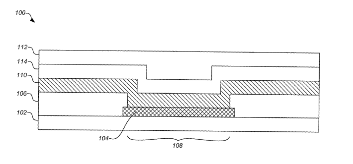
layer. FIG. 1
illustrates a cross-section of a typical sensor structure 100 of the present
invention. The
sensor is formed from a plurality of layers of various conductive and non-
conductive
constituents disposed on each other according to a method of the invention to
produce a
8
CA 02502277 2005-04-13
WO 2004/036183 PCT/US2003/033065
sensor structure 100.
A preferred embodiment of the invention is shown in FIG. 1. This embodiment
includes an electrically insulating base layer 102 to support the sensor 100.
The
electrically insulating layer base 102 can be made of a material such as a
polyimide
substrate, which may be self supporting or further supported by another
material as is
known in the art. In one embodiment, the electrically insulating layer 102
comprises a
polyimide tape, dispensed from a reel. Providing the layer 102 in this form
can facilitate
clean, high density mass production. Further, in some production processes
using such a
polyimide tape, sensors 100 can be produced on both sides of the tape.
Typical embodiments of the invention include a sensor layer disposed on the
base layer 102. In a preferred embodiment as shown in FIG. 1 the sensor layer
comprises a conductive layer 104 which is disposed on insulating base layer
102.
Preferably the conductive layer 104 comprises one or more electrodes. The
conductive
layer 104 can be applied using many known techniques and materials as will be
described
hereafter, however, the electrical circuit of the sensor 100 is typically
defined by etching
the disposed conductive layer 104 into a desired pattern of conductive paths.
A typical
electrical circuit for the sensor 100 comprises two ox more adjacent
conductive paths
with regions at a proximal end to form contact pads and regions at a distal
end to form
sensor electrodes. An electrically insulating protective layer 106 such as a
polymer
coating is typically disposed on portions of the conductive layer 104.
Acceptable
polymer coatings for use as the insulating protective layer 106 can include,
but are not
limited to, non-toxic biocompatible polymers such as polyimide, biocompatible
solder
masks, epoxy acrylate copolymers, or the like. Further, these coatings can be
photo
imageable to facilitate photolithographic forming of apertures 108 through to
the
conductive layer 104.
In the sensors of the present invention, one or more exposed regions or
apertures 108 can be made through the protective layer 106 to the conductive
layer 104
to define the contact pads and electrodes of the sensor 100. In addition to
photolithograplv.c development, the apertures 108 can be formed by a number of
techniques, including laser ablation, chemical milling or etching ox the like.
A secondary
9
CA 02502277 2005-04-13
WO 2004/036183 PCT/US2003/033065
photoresist can also be applied to the protective layer 106 to define the
regions of the
protective layer to be removed to form the apertures 108. An operating sensor
100
typically includes a plurality of electrodes such as a working electrode and a
counter
electrode electrically isolated from each other, however typically situated in
close
proximity to one another. Other embodiments may also include a reference
electrode.
Still other embodiments may utilize an separate reference not formed on the
sensor. The
exposed electrodes and/or contact pads can also undergo secondary processing
through
the apertures 108, such as additional plating processing, to prepare the
surfaces and/or
strengthen the conductive regions.
A dvn sensor chemistry layer 110 is typically disposed on one or more of the
exposed electzodes of the conductive layer 104 through the apertures 108.
Preferably,
the sensor chemistry layer 110 is an enzyme layer. Most preferably, the sensor
chemistry
layer 110 comprises the enzyme glucose oxidase. In such embodiments, the
sensor
chemistry layer 110 reacts with glucose to produce hydrogen peroxide which
modulates a
current to the electrode which can be monitored to measure an amount of
glucose
present. The sensor chemistry layer 110 can be applied over portions of the
sensor layer
or over the entire region of the sensor layer, including the protective layer
106 as shown
in FIG. 1. Preferably the sensor chemistry layer 110 is disposed on portions
of a working
electrode and a counter electrode that comprise the sensor layer. Preferred
methods fox
generating the thin sensor chemistry layer 110 include spin coating processes,
dip and dry
processes, low shear spraying processes, ink-jet printing processes, silk
screen processes
and the like. Most preferably the thin sensor chemistry layer 110 is applied
using a spin
coating process.
Typically, the thin sensor chemistry layer 110 is coated with one or more
cover
layers. In preferred embodiments of the invention, the cover layer comprises a
membrane which can regulate the aanount of analyte that can contact the enzyme
of the
sensor layer. Fox example, the cover layer can comprise a glucose limiting
membrane,
which regulates the amount of glucose that contacts the glucose oxidase enzyme
layer on
an electrode. Such glucose limiting membranes can be made from a wide variety
of
materials known to be suitable for such purposes, e.g., silicone,
polyurethane, polyurea
r
CA 02502277 2005-04-13
WO 2004/036183 PCT/US2003/033065
cellulose acetate, Nafion, polyester sulfonic acid (Kodak AQ), hydxogels or
any other
membrane known to those skilled in the art.
In preferred embodiments of the invention, the cover layer is a glucose
limiting
membrane layer 112 which is disposed above the sensor chemistry layer 110 to
regulate
S glucose contact with the sensor chemistry layer 110. In some embodiments of
; the
invention, an adhesion promoter layer 114 is disposed between the membrane
layer 112
and the sensor chemistry layer 110 as shown 'vl FIG. 1 iii order to facilitate
their contact
and/or adhesion. The adhesion promoter layer 114 can be made from any one of a
wide
variety of materials known in the art to Facilitate the bonding between such
layers.
Preferably, the adhesion promoter layer 114 comprises a silane compound. In
alternative
embodiments, protein or like molecules in the sensor chemistry layer 110 can
be
sufficiently crosslinked or otherwise prepared to allow the membrane layer 112
to be
disposed in direct contact with the sensor chemistry layer 110 in the absence
of an
adhesion promoter layer 114.
The sensors of the invention can have any desired configuration, fox example
planar or cyftndxical. The base layer 102 can be self supportive, such as a
rigid polymeric
layer, or non-self supportive, such as a flexible film. The latter embodiment
is desirable
in that it permits continuous manufacture of sensors using, for example, a
roll of a
polymeric film which is continuously unwound and upon which sensor elements,
cover
layers and functional coating layers are continuously applied.
As noted above, embodiments of the invention typically include a sensor layer
having one or more sensor elements. According to the present invention, useful
sensor
elements (referred to herein as conductive elements) include thin film
conductors ox
other electrically conductive elements that produce detectable electrical
signals.
Preferably, such conductive elements axe electrodes. Preferably, an enzyme,
such as
glucose oxidase, is disposed in the aperture 108 defined above the sensor
element.
According to a specific preferred embodiment, the sensor element is an
electrically conductive sensor element. However, sensor elements of the
present
invention are not lirxiited to conductive elements. Other useful sensor
elements can be
formed from any material that is capable of producing a detectable signal
after interacting
11
CA 02502277 2005-04-13
WO 2004/036183 PCT/US2003/033065
with a preselected analyte whose presence is to be detected (referred to
herein as reactive
elements). The detectable signal can be, for example, an optically detectable
change,
such as a color change or a visible accumulation of the desired analyte (e.g.,
cells).
Exemplary materials include polymers that bind specific types of cells; single-
strand
DNA; antigens; antibodies and reactive fragments thereof; etc. Sensor elements
can also
be formed from materials that are essentially non-reactive (i.e., controls).
The foregoing
alternative sensor elements are beneficially included, for example, in sensors
for use in
cell-sorting assays and assays for the presence of pathogenic organisms, such
as viruses
(HIV, hepatitis-C, etc.), bacteria, protozoa and the like.
Embodiments of the present invention can include one or more functional
coating
layers. As used herein, the term "functional coating layer" denotes a layer
that coats at
least a portion of at least one surface of a sensor, more preferably
substantially all of a
surface of the sensor, and that is capable of interacting with one or more
analytes, such
as chemical compounds, cells and fragments thereof, etc., in the environment
in which
the sensor is disposed. Non-limiting examples of functional coating layers
include sensor
chemistry layers (e.g., enzyme layers), analyte limiting layers, biocompatible
layers; layers
that increase the slipperiness of the sensor; layers that promote cellular
attachment to the
sensor; layers that reduce cellular attachment to the sensor; and the like.
Typically
analyte limiting layers operate to prevent or restrict the diffusion of one or
more analytes,
such as glucose, through the layers. Optionally such layers can be formed to
prevent or
restrict the diffusion of one type of molecule through the layer (e.g.
glucose), while at the
same time allowing or even facilitating the diffusion of other types of
molecules through
the layer (e.g. Oz). An illustrative functional coating layer is a hydrogel
such as those
disclosed in U.S. Patent Nos. 5,786,439 and 5,391,250, the disclosures of each
being
incorporated herein by reference. The hydrogels described therein are
particularly useful
with a variety of implantable devices for which it is advantageous to provide
a
surrounding water layer.
The sensor embodiments disclosed herein can include layers having UV-
absorbing polymers. In accordance with one aspect of the present invention,
there is
provided a sensor including at least one functional coating layer including a
UV-
12
CA 02502277 2005-04-13
WO 2004/036183 PCT/US2003/033065
absorbing polymer. In preferred embodiments, the UV-absorbing polymer is a
polyurethane, a polyuxea ox a polyuxethane/polyurea copolymer. More
preferably, the
selected UV-absorbing polymer is formed from a reaction mixture including a
diisocyanate, at least one diol, diainine or mixture thereof, and a
polyfunctional UV
absorbing monomer.
UV-absorbing polymers are used with advantage in a variety of sensor
fabrication
methods, such as those described in U.S. Pat. No. 5,390,671, to Lord et al.,
entitled
"Transcutaneous Sensor Insertion Set"; No. 5,165,407, to Wilson et al.,
entitled
"Implantable Glucose Sensor"; and U.S. Pat. No. 4,890,620, to Gough, entitled
"Two-
Dimensional Diffusion Glucose Substrate Sensing Electrode", which are
incorporated
herein in their entireties by reference. However, any sensor production method
which
includes the step of forming a UV-absorbing polymer layer above ox below a
sensor
element is considered to be within the scope of the present invention. In
particular, the
inventive methods axe not limited to thin-film fabrication methods, and can
work with
other sensor fabrication methods that utilize UV-laser cutting. Embodiments
can work
with tlvck-film, planar ox cylindrical sensors and the like, and other sensor
shapes
requiring laser cutting.
As disclosed herein, the sensors of the present invention are particularly
designed
for use as subcutaneous ox txanscutaneous glucose sensors for monitoring blood
glucose
levels in a diabetic patient. Typically each sensor comprises a plurality of
sensor
elements, for example electrically conductive elements such as elongated thin
film
conductors, formed between an underlying insulative thin film base layer and
an
overlying insulative thin film cover layer.
If desired, a plurality of different sensor elements can be included in a
single
sensor. For example, both conductive and reactive sensor elements can be
combined in
one sensor, optionally with each sensor element being disposed on a different
portion of
the base layer. One or more control elements can also be provided. In such
embodiments, the sensor can have defined in its cover layer a plurality of
openings ox
apertures. One or more openings can also be defined in the cover layer
directly over a
portion of the base layer, in order to provide for interaction of the base
layer with one or
13
CA 02502277 2005-04-13
WO 2004/036183 PCT/US2003/033065
more analytes in the environment in which the sensor is disposed. The base and
cover
layers can be comprised of a vaxiety of materials, typically polymers. In more
specific
embodiments the base and cover layers are comprised of an insulative material
such as a
polyicoide. Openings are typically formed in the cover layer to expose distal
end
electrodes and proximal end contact pads. In a glucose monitoring application,
for
example, the sensor is placed transcutaneously so that the distal end
electrodes are in
contact with patient blood or extracellular fluid, and the contact pads axe
disposed
externally for convenient connection to a monitoring device.
An illustrative embodiment of the invention is a sensor designed for
implantation
within a body that comprises a base layer, a sensor layer disposed upon the
base layer
which includes a plurality of sensor elements, an enzyme layer (preferably
less than 2
microns in thickness) disposed upon the sensor layer which coats all of the
plurality of
sensing elements on the sensor layer, and a cover layer. Typically the enzyme
layer
comprises glucose oxidase, preferably in a substantially fixed ratio with a
carrier protein.
In a specific embodiment, the glucose oxidase and the carrier protein are
distributed in a
substantially uniform manner throughout the disposed enzyme layer. Typically
the
carrier protein comprises albumin, preferably in an amount of about 5% by
weight. As
used herein, "albumin" refers to those albumin proteins typically used by
artisans to
stabilize polypeptide compositions such as human senun albumin, bovine serum
albumin
and the like. In highly preferred embodiments of the invention, the cover
layer is an
analyte contacting layer which is disposed on the sensor so as to regulate the
amount of
analyte that can contact the enzyme-layer. In further highly preferred
embodiments, the
sensor includes an adhesion promoter layer disposed between the enzyme layer
and the
analyte contacting layer and the enzyme layer is less than 1, 0.5, 0.25 or 0.1
microns in
thickness.
A related embodiment of the invention is an electrochemical analyte sensor
which includes a base layer, a sensor layer disposed upon the base layer that
includes at
least one working electrode and at least one counter electrode, an enzyme
layer disposed
upon the sensor layer, wherein the enzyme layer is less than 2 microns in
thickness; and
an analyte contacting layer that regulates the amount of analyte that contacts
the enzyme
14
CA 02502277 2005-04-13
WO 2004/036183 PCT/US2003/033065
layer. In a specific embodiment of the invention, the working electrode and/or
the
coated surface of the working electrode is larger than counter electrode
and/or the
coated surface of the counter electrode. In preferred embodiments, the enzyme
layer
comprises glucose oxidase stabilized by coating it on the working electrode
and the
counter electrode in combination with a carrier protein in a fixed ratio. In a
highly
preferred embodiment, the enzyme layer substantially covers the sensor layer.
Embodiments where the glucose oxidase enzyme layer is disposed in a uniform
coating
over the whole sensor layer are preferred because they may avoid problems
associated
with sensors having multiple different coatings on a single layer such as the
selective
delamination of different coatings having different material properties.
Optionally, the
sensor includes an adhesion promoting layer disposed between the enzyme layer
and the
analyte contacting layer.
A related embodiment of the invention is an electrochemical analyte sensor
which includes a base layer, a sensor layer disposed upon the base layer that
includes at
least one working electrode, at least one reference electrode and at least one
counter
electrode, an enzyme layer disposed upon the sensor layer, and an analyte
contacting
cover layer that regulates the amount of analyte that contacts the enzyme
layer. In
preferred embodiments, the enzyme layer is less than 2 microns in thickness
and is
coated on at least a portion of the working electrode, the reference electrode
and the
counter electrode. In a highly preferred embodiment, the enzyme layer
substantially
covers the working electrode, the reference electrode and the counter
electrode.
Optionally, the enzyme layer comprises glucose oxidase in combination with a
carrier
protein (e.g, albumin) in a fixed ratio. Typically, the sensor includes an
adhesion
promoting layer disposed between the enzyme layer and the analyte contacting
layer.
Yet another embodiment of the invention comprises a glucose sensor for
implantation within a body which includes a base layer, a sensor layer
disposed upon the
base layer, a glucose oxidase layer disposed upon the sensor layer, wherein
the glucose
oxidase is stabilized by combining it with albumin in a defined ratio and
further wherein
the glucose oxidase and the albumin are distributed in a substantially uniform
manner
throughout the disposed layer, and a glucose limiting layer that regulates the
amount of
CA 02502277 2005-04-13
WO 2004/036183 PCT/US2003/033065
glucose that contacts the glucose oxidase layer. In preferred embodiments, the
sensor
layer includes a plurality of sensor elements including at least one working
electrode and
at least one counter electrode. In such sensor embodiments, the glucose
oxidase layer is
preferably less than 2, 1, 0.5, 0.25 or 0.1 microns in thickness and the
albl»'!'m?n in the
layer is present in an amount of about 5% albumin by weight. Preferably the
sensor
includes an adhesion promoting layer disposed between the glucose oxidase
layer and the
glucose )uniting layer.
A highly preferred embodiment of the invention is an electrochemical glucose
sensor having hydrogen peroxide recycling capabilities. Typically such sensors
include a
, base layer, a sensor layer disposed upon the base layer, wherein the sensor
layer includes
at least one working electrode and at least one counter electrode, a glucose
oxidase layer
disposed upon the sensor layer, wherein the glucose oxidase layer coats at
least a portion
of the working electrode and at least a portion of the counter electrode in a
manner such
that the working electrode oxidizes hydrogen peroxide that is produced by
glucose
oxidase upon reaction with glucose, and a glucose limiting layer disposed on
the sensor
so as to regulate the amount of glucose that can contact the glucose oxidase
layer and to
inhibit die diffusion of hydrogen peroxide into the environment in which the
sensor is
placed. Typically such sensors include an adhesion promoting layer disposed
between
the glucose oxidase layer and the glucose limiting layer. In addition such
sensors usually
include an insulation layer between the base layer and the glucose oxidase
layer. The
embodiments of the invention relating to electrochemical glucose sensors
having
hydrogen peroxide recycling capabilities are particularly preferred because
the recycling
of this molecule reduces the amount of hydrogen peroxide that can escape from
the
sensor into the environment in which it is placed. In this context,
implantable sensors
that are designed to reduce the release of tissue irritants such as hydrogen
peroxide will
have improved biocompatibility profiles. Consequently, yet another embodiment
of the
invention is a method of improving the biocompatibility of a glucose oxidase
sensor by
designing the sensor to incorporate the hydrogen peroxide recycling elements
disclosed
herein.
In certain embodiments of the invention disclosed herein (e.g., those having
1G
CA 02502277 2005-04-13
WO 2004/036183 PCT/US2003/033065
hydrogen peroxide recycling capabilities) the sensor layer has a plurality of
electzodes
including a working electrode and a counter electrode, both of which are
coated with a
layer of glucose oxidase. Such sensor designs have surprising properties
including an
enhanced sensitivity. Without being bound by a specific theory, these
properties may
result from the enhanced oxidation of hydrogen peroxide at the surface of the
electrode
which produces additional oxygen that can be utilized in the glucose sensing
reaction
(see, e.g., FIG. 2). Therefore this recycling effect may reduce the oxygen
dependent
limitations of such sensors. Moreover, this design may result in a sensor
having a
counter electrode that can readily reduce available hydrogen peroxide and
consequently
has a lower electrode potential. Sensors designed to function with lower
electrode
potentials are preferred embodiments of the invention because high electrode
potentials
in sensors of this type can result in a gas producing hydrolysis reaction
which can
destabilize the sensors (due to the disruption of sensor layers from gas
bubbles produced
by hydrolysis reactions). In addition, in sensor embodiments designed so that
the
counter electrode is coated with a very thin layer of glucose oxidase, the
hydrogen
peroxide generated when glucose reacts with glucose oxidase is very close to
the reactive
surface of the counter electrode. This can increase the overall efficiency of
the sensor in
a manner that allows for the production of compact sensor designs which
include for
example, counter electrodes with smaller reactive surfaces.
A variety of art-accepted methods and materials can be utilized to generate
such
sensors. For example, while a variety adhesion promoting compounds axe known
in the
art, typically this layer comprises a silane compound. In preferred
embodiments of the
invention, the base layer comprises a polyixnmide, the insulation layer
comprises a
polyimmide, an electrode comprises platinum black and the glucose limiting
layer
comprises a hydroplvlic polymer. Preferably, the glucose oxidase layer is
vapor
crosslinked on the sensor layer.
C. METHODS FOR PRODUCING ANALYTE SENSORS OF THE INVENTION
The disclosure provided herein teaches methods for applying very thin enzyme
coatings to these types of sensors as well as sensors produced by such
processes. In this
17
CA 02502277 2005-04-13
WO 2004/036183 PCT/US2003/033065
context, preferred embodiments of the invention include methods for making
such
sensors on a substrate according to art accepted processes. In certain
embodiments, the
substrate comprises a rigid and flat structure suitable for use in
photolithogxaphic mask
and etch processes. In this regard, the substrate typically defines an upper
surface having
a high degs:ee of uniform flatness. A polished glass plate may be used to
define the
smooth upper surface. Alternative substrate materials include, for example,
stainless
steel, aluminum, and plastic materials such as delrin, etc. In other
embodiments, the
substrate is non-rigid and can be another layer of filth or insulation that is
used as a
substrate, fox example plastics such as polyi~nides and the like.
An W itial step in the methods of the invention t~rpically includes the
formation of
a base layer of the sensor. The base layer can be disposed on the substrate by
any desired
means, fox example by controlled spin coating. In addition, an adhesive may be
used if
there is not sufficient adhesion between the substrate layer and the base
layer. A base
layer of insulative material is formed on the substrate, typically by applying
the base layer
material onto the substrate in liquid form and thereafter spinning the
substrate to yield
fine base layer of thin, substantially uniform thickness. These steps are
repeated to build
up the base layer of sufficient thickness, followed by a sequence of
photolithogxaphic
and jor chemical mask and etch steps to form the conductors discussed below.
In a
preferred form, the base layer comprises a thin film sheet of insulative
material, such as
polyicoide having a filin thickness on the order of about 0.003 inch.
The methods of the invention further include the generation of a. sensor layer
having one or more sensor elements. Typically these sensor elements are
electrodes that
are formed by one of the variety of methods known in the art such as
photoresist,
etching and rinsing to define the geometry of the active electrodes. The
electrodes can
then be made electrochemically active, for example by elect~odeposition of Pt
'black for
the working and counter electrode, and silver followed by silver chloride on
the reference
electrode. The enzyme layer is then disposed on the sensor layer by a method
other than
electrochemical deposition, followed by vapor cxosslinking, for example with a
dialdehyde (glutaraldehyde) ox a carbodi-imide.
In an exemplary embodiment of the invention, the base layer is initially
coated
I
18
CA 02502277 2005-04-13
WO 2004/036183 PCT/US2003/033065
with a thin film conductive layer by electrode deposition, surface sputtering,
or other
suitable process step. In the preferred form, this conductive layer may be
provided as a
plurality of thin film conductive layers, such as an initial chrome-based
layer suitable for
chemical adhesion to a polyicoide base layer followed by subsequent formation
of thin
film gold-based and chrome-based layers in sequence. In alternative
embodiments, other
electrode layer conformations or materials can be used. The conductive layer
is then
covered,-in accordance with conventional photolithographic techniques, with a
selected
photoxesist coating, and a contact mask can be applied over the photoresist
coating fox
suitable photoimaging. The contact mask typically includes one ox more
conductor trace
patterns for appropriate exposure of the photoresist coating, followed by an
etch step
resulting in a plurality of conductive sensor traces remaining on the base
layer. In an
illustrative sensor construction designed for use as a subcutaneous glucose
sensor, each
sensor trace can include three parallel sensor elements corresponding with
three separate
electrodes such as a working electrode, a counter electrode and a reference
electrode.
Portions of the conductive sensors axe typically covered by a insulative
layer,
preferably of a material such as a polyicoide. The insulative layer can be
applied in any
desired manner. In an exemplary procedure, the insulative layer is applied in
a liquid
layer over the sensor traces, after which the substrate is spun to distribute
the liquid
material as a thin film overlying the sensor traces and extending beyond the
marginal
edges of the sensor traces in sealed contact with the base layer. This liquid
material can
then be subjected to one or more suitable radiation and/or chemical and/or
heat curing
steps as axe known in the art. In alternative embodiments, the liquid material
can be
applied using spray techniques ox any other desired means of application.
Various
insulative layer materials may be used such as photoixnagable epoxyacrylate,
with a
preferred material comprising a photoimagable polyicoide available from OCG,
Inc. of
West Patexson, N.J., under the product number 7020.
Appropriate electrode chemistries defining the distal end electrodes can be
applied to the sensor tips, optionally subsequent to exposure of the sensor
tips through
the openings. In an illustrative sensor embodiment having three electrodes for
use as a
glucose sensor, an enzyme (preferably glucose oxidase) is provided within one
of the
19
CA 02502277 2005-04-13
WO 2004/036183 PCT/US2003/033065
openings, thus coating one of the sensor tips to define a working electrode.
One ox both
of die other electrodes can be provided with d1e same coating as the working
electrode.
Alternatively, the other two electrodes can be provided with other suitable
chemistries,
such as other enzymes, left uncoated, or provided with chemistries to define a
reference
electrode and a counter electrode for the electrochemical sensor.
A significant aspect of the present invention involves processes for making
sensors having extremely thin coatings for electrode chemistries (e.g., enzyme
coatings of
less than 2 microns in thickness) with enhanced material properties. Methods
for
producing the extremely thin enzyme coatings of the invention include spin
coating
processes, dip and dry processes, low shear spraying processes, ink-jet
printing processes,
silk screen processes and the like. As artisans can readily determine the
thickness of an
enzyme coat applied by process of the art, they can readily identify those
methods
capable of generating the extremely thin coatings of the invention. Typically,
such
coatings are vapor cxosslinked subsequent to their application. Surprisingly,
sensors
produced by these processes have material properties that exceed those of
sensors having
coatings produced by electrodeposition including enhanced longevity,
linearity, regularity
as well as improved signal to noise ratios. In addition, embodiments of the
invention
that utilize glucose oxidase coatings formed by such processes are designed to
recycle
hydrogen peroxide and improve the biocompatibility profiles of such sensors.
~Xlhile not being bound by a specific scientific theory, it is believed that
the
surprising properties of sensors produced by such processes have enhanced
characteristics as compared to those generated by electrodeposition because
electrodeposition produces 3-5 micron thick enzyme layers in which only a
fraction of
the reactive enzyme is able to access the analyte to be sensed. Moreover, in
sensors
utilizing glucose oxidase, the thick coatings produced by electrodeposition
may hinder
the ability of hydrogen peroxide generated at the reactive interface to reach
the sensor
surface and thereby generate a signal. Moreover, hydrogen peroxide that is
unable to
reach a sensor surface due to such thick coatings typically diffuses away from
the sensor
into the environment in which the sensor is placed, thereby decreasing the
biocompatibility of such sensors. In addition, as glucose oxidase and albumin
have
CA 02502277 2005-04-13
WO 2004/036183 PCT/US2003/033065
different isoelectric points, electrodeposition processes can result in a
surface coating in
which an optimally determined ratio of enzyme to carrier protein is
detrimentally altered
and further wherein the glucose oxidase and the carrier protein are not
distributed in a
substantially uniform manner throughout the disposed enzyme layer. The thin
coating
processes utilized to produce the sensors disclosed herein avoid these
problems
associated with electrodeposition.
Sensors generated by processes such as spin coating processes also avoid other
problems associated with electrodeposition, such as those pertaining to the
material
stresses placed on the sensor during the electrodeposition process. In
particular, the
process of electrodeposition is observed to produce mechanical stresses on the
sensor,
for example mechanical stresses that result from tensile andjor compression
forces. In
certain contexts, such mechanical stresses may result in sensors having
coatings with
some tendency to crack or delaminate. Tllis is not observed in coatings
disposed on
sensor via spin coating or other low-stress processes. Consequently, yet
another
embodiment of the invention is a method of avoiding the electrodeposition
influenced
cracking and ox delamination of a coating on a sensor comprising applying the
coating
via a spin coating process.
Subsequent to treatment of the sensor elements, one or more additional
functional coating or cover layers can then be applied by any one of a wide
variety of
methods known in the art, such as spraying, dipping, etc. In preferred
embodiments of
the invention, the sensor is made by methods which apply a cover layer that
comprises a
hydrophilic membrane coating which can regulate the amount of analyte that can
contact
the enzyme of the sensor layer. For example, the cover layer that is added to
the glucose
sensors of the invention can comprise a glucose limiting membrane, which
regulates the
amount of glucose that contacts glucose oxidase enzyme layer on an electrode.
Such
glucose linvting membranes can be made from a wide variety of materials known
to be
suitable for such purposes, e.g., silicone, polyurethane, cellulose acetate,
Nafion,
polyester sulfonic acid (Kodak AQ), hydrogels or any other membrane known to
those
skilled in the art. In certain embodiments of the invention pertaining to
sensors having
hydrogen peroxide recycling capabilities, the membrane layer is disposed on
the glucose
21
CA 02502277 2005-04-13
WO 2004/036183 PCT/US2003/033065
oxidase enzyme layer to inhibit the release of hydrogen peroxide into the
environment in
which the sensor is placed and to facilitate the contact between the hydrogen
peroxide
molecules and the electrode sensing elements.
In some embodunents of the methods of invention, an adhesion promoter layer
is disposed between the cover layer and the sensor chemistry layer in order to
facilitate
their contact. The adhesion promoter layer can be made from any one of a wide
variety
of materials known in the art to facilitate the bonding between such layers
and can be
applied by any one of a wide variety of methods known in the art. Preferably,
the
adhesion promoter layer comprises a silane compound. Like certain other
coating layers
of the sensor, the adhesion promoter layer can then be subjected to one or
more suitable
radiation andf ox chemical and/or heat curing steps as are known in the art.
In
alternative embodiments, the enzyme layer can be sufficiently crosslinked or
otherwise
prepared to allow the membrane cover layer to be disposed in direct contact
with the
sensor chemistry layer in the absence of an adhesion promoter layer.
A preferred embodiment of the invention is a method of making a sensor by
providing a base layer, forming a sensor layer on the base layer, spin coating
an enzyme
layer on the sensor layer and then foxmixig an analyte contacting layer on the
sensor,
wherein the analyte contacting layer regulates the amount of analyte that can
contact the
enzyme layer. In preferred methods, the enzyme layer is vapor cxosslinked on
the sensor
layer. In a typical embodiment of the invention, the sensor layer is formed to
include at
least one working electrode and at least one counter electrode. In highly
preferred
embodiments, the enzyme layer is formed on at least a portion of the working
electrode
and at least a portion of the counter electrode. Typically, the enzyme layer
that is formed
on the sensor layer is less than 2, 1, 0.5, 0.25 or 0.1 microns in thickness.
Preferably, the
enzyme layer comprises glucose oxidase, glucose dehydrogenase, lactose
oxidase,
hexokinase or lactose dehydxogenase. In a specific method, the enzyme layer
comprises
glucose oxidase that is stabilized by coating it on the sensor layer in
combination with a
carrier protein in a ~txed ratio. Typically the carrier protein is albumin.
Preferably such
methods include the step of forming an adhesion promoter layer disposed
between the
glucose oxidase layer and the analyte contacting layer. Optionally, the
adhesion
22
CA 02502277 2005-04-13
WO 2004/036183 PCT/US2003/033065
promoter layer is subjected to a curing process prior to the formation of the
analyte
contacting layer.
,A related embodiment of the invention is a method of making a glucose sensor
by providing a base layer, forming a sensor layer on the base layer that
includes at least
S one working electrode and at least one counter electrode, forming a glucose
oxidase layer
on the sensor layer by a spin coating process (a layer which is preferably
stabilized by
combining the glucose oxidase with albumin in a fixed ratio), wherein the
glucose
oxidase layer coats at least a portion of the working electrode and at least a
portion of the
counter electrode, and then forming an glucose limiting layer on the glucose
sensor so as
to regulate the amount of glucose that can contact the glucose oxidase layer.
In such
processes, the glucose oxidase layer that is formed on the sensor layer is
preferably less
than 2, 1, 0.5, 0.25 or 0.1 microns in thickness. Typically, the glucose
oxidase coating is
vapor crosslinked on the sensor layer. Optionally, the glucose oxidase coating
covers the
entire sensor layer. In highly preferred embodiments of the invention, an
adhesion
promoter layer disposed between the glucose oxidase layer and the analyte
contacting
layer
The finished sensors produced by such processes are typically quickly and
easily
removed from a supporting substrate (if one is used), for example, by cutting
along a line
surrounding each sensor on the substrate. The cutting step can use methods
typically
used in this art such as those that include a W laser cutting device that is
used to cut
through the base and cover layers and the functional coating layers along a
line
surrounding or circumscribing each sensor, typically in at least slight
outward spaced
relation from the conductive elements so that the sufficient interconnected
base and
cover layer material remains to seal the side edges of the finished sensor.
Since the base
layer is typically not physically attached or only minimally adhered directly
to the
underlying supporting substrate, the sensors can be lifted quickly and easily
from the
supporting substrate, without significant further processing steps or
potential damage
due to stresses incurred by physically pulling or peeling attached sensors
from the
supporting substrate. The supporting substrate can thereafter be cleaned and
reused, or
otherwise discarded. Alternatively, the functional coating layers) can be
applied after the
23
CA 02502277 2005-04-13
WO 2004/036183 PCT/US2003/033065
sensor including base layer, sensor elements and cover layer is removed from
the
supporting substrate by cutting.
D. KITS AND SENSOR SETS OF THE INVENTION
In another embodiment of the invention, a kit and/or sensor set, useful for
the
sensing an analyte as is described above, is provided. The kit and/or sensor
set typically
comprises a container, a label and a sensor having an extremely thin enzyme
coating as
described above. Suitable containers include, for example, an easy to open
package made
from a material such as a metal foil, bottles, vials, syringes, and test
tubes. The
containers may be formed from a variety of materials such as metals (e.g.
foils) paper
products, glass or plastic. The container preferably holds a glucose sensor
coated with a
layer of glucose oxidase that is less than 2 microns in thickness. The label
on, or
associated with, the container indicates that the sensor is used for assaying
the analyte of
choice. The kit and/or sensor set may further include other materials
desirable from a
commercial and user standpoint, including elements or devices designed to
facilitate the
introduction of the sensor into the analyte environment, other buffers,
diluents, filters,
needles, syringes, and package inserts with instructions for use.
Various citations are referenced throughout the specification. In addition,
certain
text from related art is reproduced herein to more clearly delineate the
various
embodiments of the invention. The disclosures of all citations in the
specification are
expressly incorporated herein by reference.
24