Note: Descriptions are shown in the official language in which they were submitted.
CA 02502306 2005-04-14
WO 2004/038521 PCT/EP2002/011903
1
A reconfigurable state machine architecture and related
method of execution
Field of the invention
The invention relates to state machines and, more
specifically, to architectures for state machines.
Description of the related art
Evolution of microelectronics has led to highly
complex components being integrated in a single
circuit, thus giving rise to so-called systems-on-a
chip (SoC). Complex systems including co-operating
hardware and software components can thus be
manufactured that implement high-level functions.
Key features of a truly successful electronic
system are reconfigurability and the capability of
programming, possibly in run time conditions, the
functions performed by a single integrated circuit.
These features provide the circuit with a high degree
of flexibility, while permitting the circuit to be used
for different applications.
The concept of programmability has been applied to
microprocessors, where binary instructions are
translated into a set of micro-instructions (that are
fixed within the processor) for controlling operations
in the operating part of the processor, i.e. that part
of the processor where "active" elements such as
adders, multipliers, and so on are located. A first
extension of this concept leads to re-programming the
microinstruction set in order to extend the set of
instructions adapted to be implemented by the
processor. For that purpose, specialised hardware
blocks may be associated with the processor in order to
perform those functions whose degree of complexity is
beyond the current capability of a microprocessor
andlor those functions not adapted to be implemented in
a truly satisfactory manner by a microprocessor. Such
CONFIRMATION COPY
CA 02502306 2005-04-14
WO 2004/038521 PCT/EP2002/011903
2
hardware blocks are usually patterned after a fixed
configuration and generally exhibit a poor degree of
re-programmability as they are in fact designed to
fulfil a specific function.
A new concept recently introduced in the art
provides for programmability being extended also to
those hardware blocks. To obtain this, the control
parts that manage operation of the data portion of the
processor must be suitable for re-programming. Such
control parts are currently implemented via a finite
state machine or FSM.
In US-A-6 212 625 a general-purpose dynamically
programmable state engine is disclosed that dynamically
executes finite state machine and finite state machine
models. The state engine comprises an input and filter
unit, a storage unit, a transition unit, and an action
generation unit. The storage unit stores a state entry
table including a plurality of state entries. Each
state entry in the storage unit includes a state
identifier, a symbol identifier, a plurality of state
attributes, and a next state. The input and filter unit
accepts inputs and translates the inputs to symbols.
The symbols are provided to the transition unit. The
transition unit maintains a current state and locates a
state entry in the storage unit having a state
identifier matching the current state and a symbol
identifier matching a current symbol. The current state
is set to a next state of a matching entry by the
transition unit when the matching entry is a
terminating entry. G~h.en a terminating entry is
detected, an action generation unit for processing the
terminating entry is activated. A finite state machine
may be configured for execution by the state engine
using a state machine development tool.
The arrangement disclosed in US-A-6 212 625
provides for a state entry table including cells (i.e.
CA 02502306 2005-04-14
WO 2004/038521 PCT/EP2002/011903
3
addresses) each associating a single next state to a
given state identifier. Information related to possible
evolution of the machine from a given state towards a
plurality of next states, that is a current occurrence
in state machines, can thus be stored only in a
corresponding plurality of cells. Properly executing
such a state machine requires that all these cells
should be read, which inevitably takes a corresponding
plurality of clock cycles, thus slowing down machine
execution.
Another basic disadvantage of the arrangement of
US-A-6 212 625 lies in that reprogramming of the
storage unit comprising the core of the state engine
disclosed therein can only be effected via the
transition unit associated therewith, that is through
the input data channel to the transition unit and the
state machine.
Object and summary of the invention
The object of the present invention is to provide
an improved arrangement that dispenses with the
drawbacks of the prior art arrangement considered in
the foregoing.
According to the invention, that object is
achieved by means of the state machine architecture
having the features set forth in the claims that
follow. The invention also relates to a corresponding
method of executing such a state machine.
In the presently preferred embodiment, the
invention provides a re-programmable state machine
architecture adapted to be implemented by means of
volatile memories.
A presently preferred use of the architecture of
the present invention is within control units for
interface adapted for interfacing buses and
intellectual properties (IPs). However, reference to
such a possible application is for exemplary purposes
CA 02502306 2005-04-14
WO 2004/038521 PCT/EP2002/011903
4
only and must in no way be construed as limiting the
scope of the invention.
The architecture of the invention is adapted for
VHDL description at the system level and is therefore
technology-independent. In comparison with prior art
solutions, the architecture of the invention has a
parametric nature and can be easily adapted to
different configurations. The parametric nature also
facilitates implementation of optimal solutions
concerning chip area, particularly in respect of the
use of memories.
In the presently preferred embodiment, the main
parameters adapted to be selectively varied are:
- the maximum number of states;
- the maximum number of transitions from one state
towards the other states (or the same state);
- the type of machine description, that is Mealy
or Moore; and
- the number of counters used for describing the
state machine.
As is well known, in a Mealy machine the output is
determined by the inputs and the current state.
Conversely, in a Moore machine the output is determined
only by the current state while the inputs affect only
the state transitions. The parameters mentioned in the
foregoing thus have an impact on overall RAM size.
Counters can be used for following a number of
times a path through a state or a series of states. In
comparison with prior art solutions counters are
implemented externally of the machine and communicate
with the machine via an enable signal and an end of
count signal. Such signals are therefore handled as
current input and output signals of the state machine.
The description of the machine to be stored in the
memory (typically a RAM) can be appreciably reduced,
thus achieving a significant reduction in memory
CA 02502306 2005-04-14
WO 2004/038521 PCT/EP2002/011903
occupation. Programmability is ensured by making the
reference value (or the end count value) of the
counters adapted to be modified, possibly in run time
conditions. To that end each counter is provided with a
5 re-writable register containing the reference value.
This concept can be easily extended to other
computational blocks such as adders and comparators.
Brief description of the annexed drawings
The invention will now be described, by way of
example only, with reference to the annexed figures of
drawing, wherein:
- Figure 1 is a block diagram showing the general
layout of an architecture according to the invention,
- Figure 2 describes the overall arrangement of
the memory within the architecture of figure 1,
- Figure 3 is diagram further detailing
organisation and arrangement of the memory of an
architecture according to the invention, and
- Figures 4 and 5 are exemplary of the time
behaviours of certain signals generated within the
architecture of the invention.
Detailed description of a preferred embodiment of the
,." ro,., ~- ; .".,
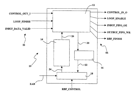
In the block diagram of figure 1 a finite state
machine (FSM) architecture according to the invention
is generally designated 10.
More specifically, the exemplary embodiment shown
in figure 1 relates to a RAM based FSM (hereinafter
RBF) including the following basic blocks:
- an output and state selector 12, the selector 12
being fed with input signals IS and adapted to generate
therefrom output signals OS;
- a basic memory block 14, in the form of a RAM;
- a state register 16; and
CA 02502306 2005-04-14
WO 2004/038521 PCT/EP2002/011903
6
- a controller 18 operating under the control of a
control signal RBF CONTROL in co-operation with an
external access bus over a line designated EAB.
Information concerning the states is transferred
from the selector 12 towards the state register 16 over
a line 20 thus permitting corresponding information to
be transferred from the register 16 to the controller
18 over a line 22. Control signals generated within the
controller 18 are transferred towards the RAM 14 over a
line 24 while a line 26 carries signals generated
within the RAM 14 towards the selector 12.
As better shown in figure 2, the memory 14 is
arranged in such a way to permit transition from a
state to another within a single cycle of the
respective clock signal CLK. In order to achieve this,
the complete description of a state must be available
at the same instant of time. Since the description of
each state is relatively long, a plurality of memory
units are provided that are operated jointly and
simultaneously selected. Each such memory unit contains
a respective portion of the description of the state.
One and only one state is associated to each
address in the RAM memory. For instance, all of the
0x0000 addresses of the RAM units include a part of the
description of state 0. The contents of the addresses
0x0000 of the various RAM units thus jointly and
completely describe state 0.
This solution is an improvement over prior art
arrangements wherein a single branch of the graph
representing the state machine is stored in each memory
cell (memory address). The arrangement described herein
requires several memory units, but this does not
represent a disadvantage since present-day technologies
(especially FPGA) provide memories having the degree of
flexibility required for that purpose. On the other
hand, a significant advantage related to the
CA 02502306 2005-04-14
WO 2004/038521 PCT/EP2002/011903
7
arrangement described here lies in the state diagram of
the machine being run through very rapidly. The various
memories are mapped on a single address plain with the
32 bit memory cells as shown in figure 2.
The description of a single state is partitioned
in different sections, each of which describes the
possible transition from that state towards another
state (see figure 3). Each transition is described in
terms of conditions on the machine input, value of the
subsequent state and values that the machine output
must take on (this last-mentioned value being required
only in the case of a Mealy machine).
There is one bit for each machine output that can
be set to 1 or 0. The next state is expressed in binary
format and used for re-addressing the memory.
Input conditions are expressed by means of two
bits for each input. In that way the condition to be
expressed can be set as input=1, input=0 or input=X,
that is as a three state value. This represents an
improvement over prior art solutions that include
conversion functions to pass from the input
configuration to configurations typical of the state
machine.
A default transition is also provided including
only the next state and the output values. This
transition is selected if none of the input condition
on the other transition inputs is met. In the case of
in an implementation in the form of a Moore machine to
each transition there is associated the output value of
the default transition.
By referring again to the block diagram of figure
1 the state register 16 contains the present state and
is adapted to re-address the memory 14.
The controller 18 manages accesses to the R.AM 14
and, more generally, operation of the RBF 10.
CA 02502306 2005-04-14
WO 2004/038521 PCT/EP2002/011903
8
During normal operation, the controller 18 causes
the value of the state register 16 to address the
memory 14.
Following a request from outside (RBF_CONTROL),
the controller 18 can standby, reset or pause the RBF
flow. These controls ensure a high degree of
flexibility without making the architecture unduly
complicated.
The controller 18 is adapted to manage re
programming of the RBF 10 in a situation where the
memory 14 is no longer addressed by resorting to the
state register 16, but is completely controlled from
outside.
Specifically, upon receiving a re-programming
command (RBF CONTROL), the controller 18 can standby
the RBF 10 and "open" the loop that during normal
operation causes the value of the state register 16 to
address the memory 14.
At this point, the memory is no longer addressed
by the state register 16 but is set to a condition
where the contents of the memory 14 can be modified, to
effect the desired reprogramming function, on the basis
of reprogramming signals received over the EAB line,
that is from outside the state machine.
Also, the controller 18 can act on the state
register 16 to reset the contents thereof or cause the
state register 16 to recycle through the same value to
pause operation of the RBF 10.
In one embodiment of the invention, the RBF
architecture 10 is organised around the RAM memory 14
with few addresses and long words. Each memory address
corresponds to a state and the address content
describes the state. V~hen a state is selected, the
state description is combined with the input to
determine the next state and the output. The RBF flow
CA 02502306 2005-04-14
WO 2004/038521 PCT/EP2002/011903
9
can be started, paused and reset through external
signals (RBF CONTROL).
Figure 1 lists all the inputs and outputs in
connection with possible use of the RBF 10 within a
control unit for an interface for interfacing via
respective buffers (not shown) a bus and an
Intellectual Property (IP).
Specifically, CONTROL_OUT_I indicates a signal
representative of the inputs controlling operation of
the IP. LOOP FINISH represents the end-of-count signals
of the counters associated with the RBF 10, while
INBUF DATA VALID indicates that the output signals from
the buffer from the bus to the IP are accessible
(valid).
CONTROL-IN 0 represents the signals from the IP,
LOOP ENABLE are the start count signals from the
counters, and INBUF FIFO OE is the signal that
activates reading of signals from the buffer from the
bus to the IP. OUTBUF FIFO WR is the signal that
activates writing of signals into the buffer from the
IP to the bus. Finally, RBF FINISH is the signal
indicating that the RBF has completed running through
its states.
The RBF has direct control on the IP control
signals (CONTROL_IN O and CONTROL OUT-I). The number of
these signals can be chosen via the CONTROL_IN SIGNALS
and CONTROL OUT SIGNALS parameters.
The signals LOOP FINISH and LOOP-ENABLE (whose
number is set with the LOOP COUNTERS parameter) allow
the RBF 10 to use external counters. To avoid expanding
the RAM 14, counters are implemented outside the RBF
main architecture. To enable operation of the
respective counter the RBF 10 must drive high the
LOOP ENABLE signal corresponding to the suited counter
until it responds driving high the LOOP FINISH signal.
CA 02502306 2005-04-14
WO 2004/038521 PCT/EP2002/011903
Figure 4 shows that the LOOP ENABLE signal must be
asserted for LV<i> + 2 clock cycles and also during the
last cycle when LOOP FINISH is asserted. Failing to
respect this protocol may cause internal failure.
5 The INBUF DATA VALID signal is internally driven
high when Inbuffer data are ready to be strobed on the
IP input port after an INBUF_FIFO OE request. The data
is put on the port one cycle after the INBUF DATA VALID
has been driven high. User can program the RBF 10 to
10 drive one of the CONTROL_IN 0 signals as a data
validation signal, after the INBUF DATA VALID has been
driven high.
Figure 5 shows Inbuffer data read timings.
INBUF FIFO OE can be driven by the RBF. After a given
latency the data are put on the IP input port.
INBUF DATA_VALID switches one cycle before so a
validation data signal can be driven if necessary on a
particular pin in the CONTROL_IN_0 port.
The total amount of states is limited by the
STATE NUMBER parameter whose maximal value can be e.g.
64. This means that the RAM cannot be longer than 64
cells. The cell size can be very high, especially when
there are many possible transitions from one state to
the others. For that reason the user can define the
maximal number of transitions from one state to the
others to optimise memory usage.
This is done by setting the parameter
TRANSITION PER STATE (whose maximal value can be e.g.
equal to 7). Also, the user can choose between a Mealy
and Moore implementation for the RBF 10: this may be
done e.g. by means of the MEALY NOT MOORE parameter.
The former choice requires more memory but allows more
flexible programs. The latter choice normally requires
more states to be defined but occupies less memory.
The following formula gives the RBF word length:
STATE DESCRIPTION DIM=RBF OUTPUT+STATE_DIM+
CA 02502306 2005-04-14
WO 2004/038521 PCT/EP2002/011903
11
TRANSITION PER STATE*(2*RBF_INPUT+STATE DIM+MEALY NOT MOORE*
RBF OUTPUT)
where
S RBF OUTPUT= CONTROL IN SIGNALS+LOOP COUNTERS+3
STATE DIM=[log2(STATE_NUN~ER)]
RBF INPUT=CONTROL OUT SIGNALS+LOOP COUNTERS+1
The RBF RAM 14 is preferably implemented as a set
of 32 bits word RAM accessed at the same time.
As shown in detail in Figure 2 the binary code in
RBF 10 is structured over several binary words whose
lengths depend on the RBF parameters, while the number
of words depends on the number of states. Nevertheless
the binary code is downloaded in the RAM 14 of the RBF
10 through the 32 bit bus before running the process;
for that reason the code can be reorganised on a 32 bit
basis as shown in the example.
The state description is filled with zeros to
reach a whole bit number that is a multiple of 32. The
new word is split into several 32-bit words. The most
significant words are placed at the beginning of the
memory plan, empty addresses are added to align the
words and then the other parts follow. Setting the
STATE-NUMBER signal as a power of 2 is preferred as
this avoids adding empty addresses. RBF memory
organisation as shown in Figure 2 provides for 5 states
and 112 bits for each state.
An executable program automatically generates the
RBF binary code as well as its memory organisation. The
input to this program contains all the RBF parameters
inputs as well as the state machine description. The
complete format is shown hereinbelow.
3S #RBF PARAMETERS
CONTROL IN SIGNALS= x
CA 02502306 2005-04-14
WO 2004/038521 PCT/EP2002/011903
12
CONTROL OUT SIGNALS = y
NUMBER OF STATES = s
MAX TRANSITION PER STATE= t
MEALY NOT MOORE= m
S LOOP COUNTERS= 1
#OUTPUT NAMES DEFINITION
0 RBF FINISH
1 OUTBUF FIFO WR 0
lO 2 INBUF FIFO OE I
3 LOOP COUNTERS ON 1
4 <ip input control signal>
<ip input control signal>
# INPUT NAMES DEFINITION
O INBUF DATA VALID I
1 LOOP COUNTERS FINISH <1>
2 <ip output control signal>
3 <ip output control signal>
#state <i>
cond: <input signal> <value>
<input signal> <value>
output: <output signal> 1
<output signal> 1
nextstate: <state number>
output: <output signal> 1
nextstate: <state_number>
In the first part, the parameters are declared.
CA 02502306 2005-04-14
WO 2004/038521 PCT/EP2002/011903
13
The second part contains the output signal name
definitions. Then the loop counter enable signals
definition is to be provided; the number of these
instances may change according to the LOOP COUNTERS
value (maximum value - 4). Then the IP input control
signals must be declared (up to CONTROL_IN SIGNALS
value). The first signal declared is connected to the
pin CONTROL_IN SIGNALS_O (0), the second one to the pin
CONTROL_IN SIGNALS 0 (1) and so on.
The third part contains the input signal names
definitions. Then the loop counter finish signals must
be defined; the number of these instances can change
according to the LOOP COUNTERS value (maximum value 4).
Then the IP output control signals must be declared (up
to CONTROL OUT SIGNALS value). The first signal
declared is connected to the pin CONTROL OUT SIGNAL_I
(0), the second one to the pin CONTROL OUT SIGNALS-I
(1) and so on.
After all the definitions the RBF behaviour is
described. There must be as many #state <i> instances as
NUMBER OF STATES, with <i> varying from 0 to
NUMBER OF STATES - 1. For each state all the possible
transitions are declared. Each transition declaration
preferably includes three statements, namely: the
condition that must be verified for the transition to
occur, the output signals (for a Mealy machine) that
must be set to one (the other signals will be
automatically set to 0), and the next state. There can
be as many transition declarations as
MAX_TRANSITION-PER STATE.
In addition to these declarations, a default
transition, including the output signals and the next
state, is defined to occur if all the conditions
declared are not verified. If a Moore machine is
implemented, the default transition output signals
refer to the entire state.
CA 02502306 2005-04-14
WO 2004/038521 PCT/EP2002/011903
14
A feature of the architecture described herein is
the parametric nature of the selector 12. Depending on
the size of the state description and the number of
inputs to the selector a certain number of comparators
are provided. Each comparator receives as its input all
the input signals to the state machine as well as one
of the possible input configurations described in the
state description. If one of the comparators provides a
positive result, the next state and the corresponding
output are selected. Otherwise, default values are
selected.
The state machine corresponding to the
architecture just described can be used in different
contexts and for different applications. To advantage,
it can used as an integral part of the control section
of hardware IPs.
Before execution by the RBF 10, the RAM 14 can be
re-loaded with a new configuration. The development of
the binary code for storage in the RAM 14 may be
supported by a development tool that generates the
binary code to be loaded into the RAM 14 starting from
the conventional graphical representation of a state
machine.
Of course, without prejudice to the underlying
principle of the invention, the details and the
embodiments may vary with respect to what has been
described by way of example only without departing from
the scope of the invention as defined by the claims
that follow.