Note: Descriptions are shown in the official language in which they were submitted.
CA 02502595 2005-04-14
WO 2004/038735 PCT/SE2003/001615
1
Field ctrading material
TECHNICAL FIELD OF THE INVENTION AND PRIOR ART
The present invention relates to a field grading material con-
sisting of a polymeric matrix provided with filler particles as well
as a device for grading an electric field in high-voltage applica-
15~ Lions. The invention also relates to a method for grading an
electric field at a joint or termination of an electric power cable.
At the transition of an electric field from a first medium to a sec-
ond medium, electric stresses harmful to the electric equipment
can ensue due to a discontinuity in the electric field. In a
shielded high-voltage cable for instance, the electric field is
uniform along the cable axis and there is variation in the field
only in the radial direction. When the cable is terminated or
spliced, the shield of the cable is removed for a distance along
the cable. The removal of the shield causes a discontinuity in
the electric field at the shield end, resulting in high electric
stresses. These high stresses must be reduced in order not to
impair the expected life of the system.
The electric stresses in question can be reduced by grading the
electric field at the transition of the electric field from the first
medium to the second medium, e.g. from a shielded cable part
to a cable part where the original shield has been removed. A
number of methods have been developed and employed for this
kind of field grading. The present invention is related to so
called resistive and capacitive field grading.
CA 02502595 2005-04-14
WO 2004/038735 PCT/SE2003/001615
2
The resistive field grading can be used in alternating current as
well as direct current applications. Resistive field grading can
also be used in order to achieve field grading when voltages are
occurring in the form of impulses. In case of a cable ending of
the kind indicated above, a body having a suitable resistance is
introduced around the unshielded part of the cable in the area
closest to the shielded part of the cable and in electric contact
with the shield. When a positive voltage is applied across the
cable a current flows through the body towards the shield of the
cable, which shield is at earth potential. A resistive voltage drop
then occurs in the body, which results in a more uniform distri-
bution of the potential. This potential distribution will be more
linear if the body consists of a material exhibiting a non-linear
electrical resistance that decreases with an increasing electric
field. The closer to the edge of the shield, the higher the electric
field in the field grading body and, consequently, the lower the
electrical resistance in the body if the body exhibits such a non-
linear electrical resistance. In this way, the voltage drop along
the field grading body will become more uniformly distributed in
a body that exhibits such a non-linear electrical resistance than
in a body that does not..
The capacitive field grading i used in alternating current appli-
cations. Capacitive field grading can also be used in order to
achieve field grading when voltages are occurring in the form of
impulses. In case of a cable ending of the kind indicated above,
a body of a material having a dielectric constant higher than that
of the insulation and as low losses as possible is introduced
around the unshielded part of the cable in the area closest to
the shielded part of the cable and in electric contact with the
shield, whereby a spreading of the equipotential lines will be
achieved. Capacitive field grading properties are also desired in
a material adapted for grading the electric field in high-voltage
direct current applications so as to achieve an effective field
grading in case of suddenly occurring voltage surges.
CA 02502595 2005-04-14
WO 2004/038735 PCT/SE2003/001615
3
SUMMARY OF THE INVENTION
The object of the present invention is to provide an improved
field grading material of the type indicated in the preamble of
claim 1.
According to the invention, this object is achieved by a material
having the features of claim 1.
It has been found that the use of a filler essentially consisting of
nanoscale particles, i.e. particles having at least one dimension
smaller than or equal to 100 nm, results in percolation at a lower
filler concentration in the material as compared to a corre-
sponding material comprising a filler consisting of particles of
larger size. Thus, with the material according to the invention,
desired field grading properties can be obtained with a relatively
low concentration of filler in the matrix, implying improved
processability and improved mechanical properties of the field
grading material. The lower the concentration of filler in the ma-
trix, the better the processability and the better mechanical
properties of the field grading material.
Furthermore, the use of a filler essentially consisting of
nanoscale particles results in increased electrical breakdown
strength of the field grading material as compared to a corre-
sponding material comprising a filler consisting of particles of
larger size. The electrical breakdown strength of the field grad-
ing material also increases with decreasing filler concentration.
Consequently, the invention makes it possible to achieve a field
grading material having very high electrical breakdown strength
and thus being well suited for high-voltage applications.
In this description and the subsequent claims the term "nano-
sized particles" refers to particles having at least one dimension
smaller than or equal to 100 nm, e.g. particles having a width,
CA 02502595 2005-04-14
WO 2004/038735 PCT/SE2003/001615
4
length and/or height smaller than or equal to 100 nm. The nano-
sized particles may of course have several or all dimensions
smaller than or equal to 100 nm. The nano-sized particles may
e.g. be essentially spherical or cylindrical with a diameter
smaller than or equal to 100 nm. It is emphasised that the nano-
sized particles of the filler may have any shape as long as they
in at least one of their dimensions are smaller than or equal to
100 nm.
In this description and the subsequent claims the term "field
grading effective amount of filler particles" refers to an amount
of filler particles that is sufficient for giving the material the de-
sired field grading properties.
According to a preferred embodiment of the invention, the filler
comprises a field grading effective amount of particles having
one dimension between 2-80 nm, preferably 5-50 nm and most
preferably 5-30 nm. It has been found that the above indicated
advantages of the inventional field grading material are further
improved when the size of the filler particles decreases from 100
nm and downwards. However, it is considered that a dimension
of about 2 nm of the particles is the practical lower limit. If the
particles are smaller than that, it will be very difficult to disperse
the particles in the material and to prevent the particles from
agglomerating.
A filler exhibits an essential increase in surface area per unit
volume when the dimension of the particles in the filler de-
creases from 100 nm and downwards. The surface area per unit
volume of the filler as a function of the particle size is illustrated
in Fig 1 for spherical filler particles that are fully dispersed in a
matrix material. This increase of the surface area per unit vol
ume is believed to be an important reason for the beneficial ef
fects associated with the field grading material according to the
invention.
CA 02502595 2005-04-14
WO 2004/038735 PCT/SE2003/001615
Further preferred embodiments of the field grading material ac-
cording to the invention will appear from the dependent claims
and the subsequent description.
5 The invention also relates to a device for grading an electric
field in high-voltage applications according to claim 12.
The invention also relates to a method for grading an electric
field at a joint or termination of an electric power cable accord
ing to claim 13.
BRIEF DESCRIPTION OF THE DRAWINGS
With reference to the enclosed drawings, a more specific de
scription of embodiment examples of the invention will follow
hereinbelow.
In the drawings
Fig 1 is a diagram showing the surface area per unit volume
as a function of the particle size for particles, fully
dispersed in a matrix material, having a spherical
shape,
Fig 2 is a diagram showing the electrical resistivity of differ-
ent field grading materials as a function of filler con-
centration,
Fig 3 is a diagram showing the electrical breakdown
strength of different field grading materials as a func-
tion of filler concentration,
Fig 4 is a diagram showing the dielectric constant (permit-
tivity) of different field grading materials at 1 kHz as a
function of filler concentration,
CA 02502595 2005-04-14
WO 2004/038735 PCT/SE2003/001615
6
Fig 5 is a diagram showing the electrical resistivity of differ-
ent SiC fillers as a function of electric field strength,
and
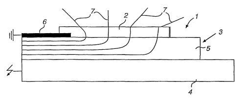
Fig 6 is a schematic -io~gitudinaf sectional of a termination
of an electric power cable, provided with a body of
field grading material according to the invention.
DETAILED DESCRIPTION OF PREFERRED EMBODIMENTS
OF THE INVENTION
The field grading material according to the present invention
consists of a polymeric matrix provided with a filler. The filler
comprises a field grading effective amount of particles having at
least one dimension smaller than or equal to 100 nm.
The surface area per unit volume of a filler comprising spherical
particles as a function of the particle size is illustrated in Fig 1.
From the diagram of Fig 1, it can be seen that a filler exhibits an
essential increase in surface area per unit volume of a fully
dispersed filler when the dimension of the particles in the filler
decreases from 100 nm and downwards. The gradient of the
curve C~ showing the surface area per unit volume of a filler as
a function of the particle size increases rapidly as the size of the
particles is gradually reduced below 100 nm. It has been found
that several important properties associated with the field grad-
ing effects of a field grading. material of the above-indicated kind
are essentially and surprisingly improved as the dimension of
the particles in the filler is reduced below 100 nm.
The polymeric matrix in the field grading material according to
the invention is suitably provided with a filler comprising a field
grading effective amount of particles having at least one dimen-
sion between 2-80 nm, preferably 5-50 nm and most preferably
5-3.0 nm.
CA 02502595 2005-04-14
WO 2004/038735 PCT/SE2003/001615
7
Fig 2 is a diagram showing the electrical resistivity of some dif-
ferent field grading materials as a function of filler concentration
(percentage by volume). A first curve C2~ is related to a field
grading material consisting of a matrix of LDPE provided with a
filler of Zn0-particles having an average size of about 0,3 pm
(300 nm). A second curve C22 is related to a field grading mate-
rial consisting of a matrix of LDPE provided with a filler of Zn0-
particles having an average size of about 49 nm. A third curve
C~3 is related to a field grading material consisting of a matrix of
LDPE provided with a filler of Zn0-particles having an average
size of about 24 nm. It is evident from this diagram that percola-
tion begins at an essentially lower filler concentration for the
materials comprising nano-sized filler particles (curves C22 and
C23) as compared to the material comprising micro-sized filler
particles (curve C2~). For the materials related to the curves C2~
and C~3 percolation begins at a filler concentration of about 12%
by volume and 15% by volume, respectively, whereas percola-
tion begins at a filler concentration of about 28% by volume for
the material related to the curve C2~. The smaller the size of the
particles, the lower the filler concentration required for per-
colation.
Fig 3 is a diagram showing the electrical breakdown strength of
two different field grading materials as a function of filler .con-
centration (percentage by volume). ~ne of the sets of measured
data points in Fig 3 is related to a field grading material con-
sisting of a matrix of LDPE provided with a filler of Zn0-particles
having an average size of about 0,3 pm (i.e. micro-sized parti-
cles). The other set of measured data points in Fig 3 is related
to a field grading material consisting of a matrix of LDPE pro-
vided with a filler of Zn0-particles having an average size of
about 50 nm (i.e. nano-sized particles). It can be seen in this
diagram that the material comprising nano-sized filler particles
has a higher electrical breakdown strength than the material
comprising micro-sized filler particles at a given filler concentra-
CA 02502595 2005-04-14
WO 2004/038735 PCT/SE2003/001615
tion. Consequently, a higher electrical breakdown strength of a
field grading material can be obtained when using nano-sized
filler particles as compared to using micro-sized filler particles.
Thus, a field grading material comprising nano-sized particles is
suitable for high-voltage applications. It can also be seen in the
diagram that the electrical breakdown strength of the respective
field grading material increases with decreasing filler concentra-
tion.
The nano-sized filler particles suitably constitute less than 40%
by volume, preferably less than 30% by volume and most pref-
erably less than 20% by volume of the field grading material.
The polymeric matrix of the field grading material according to
the present invention suitably consists, or at least essentially
consists, of rubber, thermoplastics or thermoplastic elastomer. It
is preferred that the matrix consists, or at least essentially con-
sists, of polyolefin rubber or thermoplastic polyolefin elas-
tomerlplastomer, preferably including EPDM (Ethylene Propyl-
ene Diene Monomer) rubber or silicone rubber, or of crystalline
thermoplastics, preferably polyethylene.
The nano-sized filler particles are suitably dispersed in the
polymeric matrix by ordinary melt-mixing.
According to a first variant of the invention, the filler is of a ma-
terial where the bulk has a dielectric constant at infinitely high
frequencies of at least 5, preferably A1~03, Ti02 or BaTi03. This
implies that the field grading material has effective capacitive
field grading properties in possible combination with resistive
field grading properties. It is previously known that the dielectric
constant of a material consisting of a polymeric matrix with filler
is fairly independent of the size of the high dielectric constant
particles of the filler. However, it has surprisingly been found
that there is a dramatic increase in the dielectric constant when
the, size of the particles in the filler is decreased to such an ex-
CA 02502595 2005-04-14
WO 2004/038735 PCT/SE2003/001615
9
tent that the particles have one dimension smaller than or equal
to 100 nm. Therefore, by decreasing the size of the high dielec-
tric constant particles in the filler to such an extent that the par-
ticles have one dimension smaller than or equal to 100 nm, a
field grading material having a desired dielectric constant can be
obtained with a filler concentration being essentially lower as
compared to a corresponding material comprising a filler con-
sisting of particles of larger size.
Fig 4 is a diagram showing the dielectric constant (permittivity)
of two different, field grading materials, which are subjected to
an alternating voltage having a frequency of 1 kHz, as a function
of filler concentration (percentage by volume). One of the sets of
measured data points in Fig 4 is related to a field grading
material consisting of a matrix of Engage~ provided with a filler
of A1~03-particles having an average size larger than 100 nm,
i.e. micro-sized particles. The other set of measured data points
in Fig 4 is related to a field grading material consisting of a ma-
trix of Engage~ provided with a filler of A1203-particles having an
average size of about 33 nm, i.e. nano-sized particles. It can be
seen in this diagram that the material comprising nano-sized
filler particles has a higher dielectric constant than the material
comprising micro-sized filler particles at a given filler concentra-
tion.
According to a second variant of the.invention, the filler is of a
semiconducting material, i.e. a material having an energy band-
gap larger than 0 eV and smaller than about 5 eV, preferably
Zn0 or SiC. The use of semiconducting filler materials, such as
Zn0 or SiG, normally results in a non-linear electrical resistance
of the field grading material, i.e. a resistance that decreases
with an increasing electric field. This non-linearity of the resis-
tance can be favourable in certain applications as previously
indicated. The onset of the non-linearity of the resistance, i.e.
the electrical field strength at which the resistance changes from
an .essentially linear to an essentially non-linear behaviour, in-
CA 02502595 2005-04-14
WO 2004/038735 PCT/SE2003/001615
creases with decreasing size of the particles in the filler. Thus, a
material according to this variant of the invention exhibits an
onset of the non-linearity of the resistance being at a higher
field strength as compared to a corresponding material com-
5 prising a filler consisting of particles of larger size. When the
onset of the non-linearity of the resistance is at a higher field
strength, reliable resistive field grading at high electrical fields
becomes possible. This may be combined with suitable capaci-
tive field grading properties.
Fig 5 is a diagram showing the electrical resistivity of different
SiC fillers as a function of electric field strength. One of the sets
of measured data points in Fig 5 is related to a pure SiC powder
comprising SiC particles having an average size of about 10 pm,
i.e. micro-sized particles. The other set of measured data points
in Fig 5 is related to a pure SiC powder comprising SiC particles
having an average size of about 20 nm, i.e. nano-sized
particles. It can be seen in this diagram that the material com-
prising nano-sized particles exhibits an onset of the non-linear-
ity of the resistance being at a higher electric field strength,
about 10 kV/cm, as compared to the material comprising micro-
sized particles, for which the onset of the non-linearity of the re-
sistance is below 1 kV/cm.
For a material comprising particles of micro-size and larger, the
onset of the non-linearity of the resistance is essentially recip-
rocally proportional to the particle size. It has however been no-
ticed that the onset of the non-linearity of the resistance is not
reciprocally proportional to the particle size for a material com-
prising particles of nano-size. This is advantageous since the
onset of the non-linearity of the resistance would have been at a
far too high electric field strength for a material comprising a
filler of nano-sized particles if the reciprocal proportionality had
applied also for nano-sized particles.
CA 02502595 2005-04-14
WO 2004/038735 PCT/SE2003/001615
11
According to a preferred embodiment of the invention, the nano-
sized filler particles essentially have a high aspect ratio, i.e. an
aspect ratio of more than 1, preferably more than 5 and most
preferably more than 10. Said particles may be provided in the
form of fibres, fibrils, whiskers, flakes, tubes, ellipsoids etc.
If the particles having a high aspect ratio are randomly oriented
in the matrix, an isotropic field grading material is obtained. The
use of such particles randomly oriented in the matrix results in .
percolation at a lower filler concentration as compared to a cor-
responding material comprising a filler consisting of particles
having essentially a spherical shape.
If the particles having a high aspect ratio are oriented to extend
essentially in the same direction in the matrix, i.e. if they are
oriented in a specific preferred direction in the matrix, an anisot-
ropy in field grading properties is conferred to the field grading
material, which anisotropy can be favourable in certain applica-
tions.
A field grading material according to the invention is suitable for
use at a joint or termination of an electric power cable, in which
case a body comprising the field grading material is introduced
in the cable joint or cable termination. Fig 6 schematically
illustrates a cable termination 1 provided with a body 2 of field
grading material according to the present invention. The cable 3
comprises a conductor 4 surrounded by an insulation 5. A shield
6 is arranged outside the insulation 5, said shield being con-
nected to ground. The end of the cable 3 is unshielded, i.e. at
the end of the cable the insulation 5 is not covered by any
shield. The body 2 of field grading material is introduced around
the unshielded part of the cable in the area closest to the
shielded part of the cable and in electric contact with the shield
6. The body 2 of field grading material will secure a uniform dis-
tribution of the potential at the cable termination, as illustrated
CA 02502595 2005-04-14
WO 2004/038735 PCT/SE2003/001615
12
by the equipotential lines 7 in Fig 6. Only the upper half of the
longitudinal section of the cable termination is shown in Fig 6.
A field grading material according to the invention is particularly
suitable for use in a device for grading an electric field in high-
voltage applications. Such a device could e.g. comprise a body
2 of the type illustrated in Fig 6 for use at a cable termination or
cable joint or in any other type of application where a grading of
an electric field is required.
The invention is of course not in any way limited to the preferred
embodiments described above. On the contrary, several
possibilities to modifications thereof should be evident to a per-
son skilled in the art, without deviating from the basic idea of
the invention as defined in the appended claims. It is for in-
stance possible to include an additional smaller amount of mi-
cro-sized filler particles in the matrix, as long as the essential
field grading effects are defined by the nano-sized filler particles
included in the matrix.