Note: Descriptions are shown in the official language in which they were submitted.
CA 02502850 2005-04-20
WO 2004/061974 PCT/US2003/038490
VERTICAL JFET LIMITED SILICON CARBIDE POWER METAL-OXIDE
SEMICONDUCTOR FIELD EFFECT TRANSISTORS AND METHODS OF
FABRICATING VERTICAL JFET LIMITED SILICON CARBIDE METAL-
OXIDE SEMICONDUCTOR FIELD EFFECT TRANSISTORS
Statement of Government Interest
The present invention was made, at least in part, with support from the United
States Office of Naval Research, contract number N00014-02-C-0302. The
Government may have certain rights in tlus invention.
Cross-Reference to Provisional Application
This application claims the benefit of, and priority from, Provisional
Application Serial No. 60/435,212, filed December 20, 2002 entitled hERTICAL
JFET LIMITED SILICON CARBIDE POWER METAL-OXIDE SEMICOND UCTOR
FIELD EFFECT TRANSISTORS AND METFIODS OF FABRICATING VERTICAL
JFET LIMITED SILICON CARBIDE POWER METAL-OXIDE SEMICOND UCTOR
FIELD EFFECT TRANSISTORS, the disclosure of which is hereby incorporated
herein by reference in its entirety as if set forth fully herein.
Field of the Invention
The present invention relates to semiconductor devices and the fabrication of
semiconductor devices and more particularly, to silicon carbide (SiC) metal-
oxide
semiconductor field effect transistors (MOSFETs) and the fabrication of such
MOSFETs.
Baclcaround of the Invention
To make a high current, high voltage, low on-resistance, vertical SiC power
MOSFET has, so far, been impractical, at least in part, due to the poor
surface
mobility of electrons in the inversion layer. Recently, some processing
techniques
have been developed on a lateral MOSFET structure, which result in an improved
surface electron mobility. However, a power MOSFET structure may involve
CA 02502850 2005-04-20
WO 2004/061974 PCT/US2003/038490
additional processing including, for example, anneals at temperatures of
greater than
1500° C for the activation of p-type dopants, for example, p-welllp+
contact/p-
Junction Termination Extension (JTE) implants. Such anneals may have
detrimental
impact on the performance of power MOSFETs fabricated using such techniques.
A number of silicon carbide power MOSFET structures have been described
in the literature. See e.g. U.S. Patent No. 5,506,421; A. K. Agarwal, J. B.
Casady, L.
B. Rowland, W. F. Valek, M. H. White, and C. D. Brandt, "1.1 kV 4H-SiC Power
UMOSFET's," IEEE Electron Device Letters, Vol. 18, No. 12, pp. 586-588,
December 1997; A. K. Agarwal, J. B. Casady, L. B. Rowland, W. F. Valek and C.
D.
Brandt, "1400 V 4H-SiC Power MOSFETs," Materials Science Forum Vols. 264-268,
pp. 989-992, 1998; J. Tan, J. A. Cooper, Jr., and M. R. Melloch, "High-Voltage
Accumulation-Layer UMOSFETs in 4H-SiC," IEEE Electron Device Letters, Vol. 19,
No. 12, pp. 487-489, December 1998; J. N. Shenoy, J. A. Cooper and M. R.
Melloch,
"High-Voltage Double-Implanted Power MOSFET's in 6H-SiC," IEEE Electron
Device Letters, Vol. 18, No. 3, pp. 93-95, March 1997; J. B. Casady, A. K.
Agarwal,
L. B. Rowland, W. F. Valek, and C. D. Brandt, "900 V DMOS and 1100 V UMOS
4H-SiC Power FETs," IEEE Device Research Conference, Ft. Collins, CO, June 23-
25, 1997; R. Schorner, P Friedrichs, D. Peters, H. Mitlehner, B. Weis and D.
Stephani, "Rugged Power MOSFETs in 6H-SiC with Blocking Capability up to 1800
V," Materials Science Forum Vols. 338-342, pp. 1295-1298, 2000; V. R. Vathulya
and M. H. White, "Characterization of Channel Mobility on Implanted SiC to
determine Polytype suitability for the Power DIMOS structure," Electronic
Materials
Conference, Santa Barbara, CA, June 30 - July 2, 1999; A. V. Suvorov, L. A.
Lipkin,
G. M. Johnson, R. Singh and J. W. Palmour, "4H-SiC Self Aligned Implant-
Diffused
Structure for Power DMOSFETs," Materials Science Forum Vols. 338-342, pp.
1275-1278, 2000; P. M. Shenoy and B. J. Baliga, "The Planar 6H-SiC ACCUFET: A
New High-Voltage Power MOSFET Structure," IEEE Electron Device Letters, Vol.
18, No. 12, pp. 589-591, December 1997; Ranbir Singh, Sei-Hyung Ryu and John
W.
Palmour, "High Temperature, High Current, 4H-SiC Accu-DMOSFET," Materials
Science Forum Vols. 338-342, pp. 1271-1274, 2000; Y. Wang, C. Weitzel and M.
Bhatnagar, "Accumulation-Mode SiC Power MOSFET Design Issues," Materials
Science Forum Vols. 338-342, pp. 1287-1290, 2000; and A. K. Agarwal, N. S.
Saks,
S. S. Mani, V. S. Hegde and P. A. Sanger, "Investigation of Lateral RESURF, 6H-
SiC
MOSFETs," Materials Science Forum Vols. 338-342, pp. 1307-1310, 2000.
2
CA 02502850 2005-04-20
WO 2004/061974 PCT/US2003/038490
The existing SiC structures can, generally, be divided into three categories:
(1)
Trench or UMOSFET, (2) Vertical Doubly Implanted MOSFET (DIMOSFET), and
(3) Lateral Diffused MOSFET (LDMOSFET). Of these structures, the vertical
DIMOSFET structure, illustrated in Figure 1, is a variation of the diffused
(DMOSFET) structure employed in silicon technology. Typically, the p-wells are
implanted with Al or Boron, the source regions (n+) are implanted with
nitrogen or
phosphorus, and the p+ regions are usually implanted with Al. The implants are
activated at temperatures between 1400°C - 1700°C. The contacts
to ri layers are
made with nickel (Ni) and annealed and the contacts to p+ are made by Ni, Ti
or
Ti/Al. Both contacts are annealed at high temperatures. The gate dielectric
is,
typically, either thermally grown (Thermal Si02) or deposited using Low
Pressure
Chemical Vapor Deposition (LPCVD) technique and subsequently annealed in
various ambients. The deposited dielectric may, for example, be Si02 or an
Oxide/Nitride/Oxide (ONO) stack.
The interface states near the conduction band edge tend to trap the otherwise
free electrons from the inversion layer leaving a relatively small number of
free
electrons in the inversion layer. Also the trapped electrons may create
negatively
charged states at the interface which coulomb scatter the free electrons. The
reduced
number of free electrons and the increased scattering may reduce the
conduction of
current from source to drain, which may result in low effective mobility of
electrons
and a high on-resistance. Several factors have been attributed to the high
density of
states near the conduction band edge: (1) carbon or silicon dangling bonds,
(2) carbon
clusters, and (3) Si-Si bonds creating a thin amorphous silicon layer at the
interface.
See S. T. Pantelides, "Atomic Scale Engineering of SiC Dielectric Interfaces,"
DARPA/MTO High Power and ONR Power Switching MURI Reviews, Rosslyn, VA,
August 10-12, 1999 and V. V. Afanas'ev, M. Bassler, G. Pensl, and M. Schulz,
"Intrinsic SiC/Si02 Interface States," Phys. Stat. Sol. (a), Vol. 162, pp. 321-
337, 1997.
In addition to the high density of interface states, several other mechanisms
have also been attributed to the poor mobility of inversion layer electrons:
(1) Al
segregating out of the Al-doped, p-type SiC, and (2) Surface roughness created
by the
high temperature activation of implanted impurities. See S. Sridevan, P. K.
McLarty,
and B. J. Baliga, "On the Presence of Aluminum in Thermally Grown Oxides on 6H-
Silicon Carbide," IEEE Electron Device Letters, Vol. 17, No. 3, pp. 136-138,
March
3
CA 02502850 2005-04-20
WO 2004/061974 PCT/US2003/038490
1996 and M. A. Capano, S. Ryu, J. A. Cooper, Jr., M. R. Melloch, K. Rottner,
S.
Karlsson, N. Nordell, A. Powell, and D. E. Walker, Jr., "Surface Roughening in
Ion
Implanted 4H-Silicon Carbide," Journal of Electronic Materials, Vol. 28, No.
3, pp.
214-218, March, 1999. Researchers from Purdue University have concluded that a
direct correlation exists between the inversion layer electron mobility and
the implant
activation temperature. Such research has concluded that lower implant
activation
temperature (1200°C) leads to higher electron mobility and higher
activation
temperature (1400°C) results in poor electron mobility. See M. K. Das,
J. A. Cooper,
Jr., M. R. Melloch, and M. A. Capano, "Inversion Channel Mobility in 4H- and
6H-
SiC MOSFETs," IEEE Semiconductor Interface Specialists Conference, San Diego,
CA, December 3 - 5, 1998. These results have been obtained on planar MOSFETs,
which do not utilize an implantation of the p-well. The p-well implanted
impurity (Al
or Boron) typically requires at least a 1500°C activation temperature.
A further difficulty with DIMOSFETS may be associated with the "JFET"
region of the device. As seen in Figure l, a depletion region may be formed in
the ri
drift region around the p-well. This depletion region may effectively make the
channel length longer than the p-well junction depth as current flow is
provided
around the depletion region. It has been suggested that a spacer implant be
introduced
between the p-well regions to alleviate this problem. See Vathulya et al., "A
Novel
6H-SiC DMOSFET With Implanted P-Well Spacer", IEEE Electron Device Letters,
Vol. 20, No. 7, p. 354, July 1999. This spacer implant does not extend past
the p-well
regions and does not significantly reduce the JFET resistance if the depletion
region
formed at the p-well and the n' drift region interface extends deep into the
ri drift
region.
Summary of the Invention
Embodiments of the present invention provide silicon carbide metal-oxide
semiconductor field effect transistors (MOSFETs) and methods of fabricating
silicon
carbide MOSFETs having an n-type silicon carbide drift layer, a first p-type
silicon
carbide region adjacent the drift layer and having a first n-type silicon
carbide region
therein, and an oxide layer on the drift layer. The MOSFETs also have an n-
type
silicon carbide limiting region disposed between the n-type silicon carbide
drift layer
and a portion of the first p-type silicon carbide region. In some embodiments,
the n-
4
CA 02502850 2005-04-20
WO 2004/061974 PCT/US2003/038490
type limiting region has a carrier concentration that is greater than the
carrier
concentration of the n-type silicon carbide drift layer.
In further embodiments of the present invention, the n-type silicon carbide
limiting region is provided between the drift layer and a floor of the first p-
type
silicon carbide region. In still further embodiments, the n-type limiting
region is also
provided adjacent a sidewall of the first p-type silicon carbide region. In
some
embodiments of the present invention, a portion of the limiting region
adjacent the
floor of the first p-type region has a higher carrier concentration than a
portion of the
limiting region adjacent the sidewall of the first p-type region.
In particular embodiments of the present invention, the first p-type silicon
carbide region is implanted with aluminum.
Further embodiments of the present invention provide a gate contact on the
oxide layer, a source contact on the first n-type silicon carbide layer, and a
drain
contact on the drift layer opposite the oxide layer. In particular embodiments
of the
present invention, the gate contact is polysilicon (either p-type or n-type).
In other
embodiments, the gate contact is metal. In some embodiments, an n-type silicon
carbide substrate is provided between the drift layer and the drain contact.
In certain embodiments of the present invention, the n-type limiting region is
provided by an epitaxial layer of silicon carbide on the n-type silicon
carbide drift
layer. In such embodiments, the first p-type region is provided in but not
through the
epitaxial layer of silicon carbide.
In further embodiments, the n-type limiting region is provided by an implanted
n-type region in the drift layer. In some embodiments, the n-type limiting
region has
a thickness of from about 0.5 ~,m to about 1.5 ~.m. In certain embodiments,
the n-type
limiting region has a carrier concentration of from about lx 1015 to about 5 x
101' cm
In still further embodiments of the present invention, an n-type epitaxial
layer
is provided on the first p-type region and a portion of the first n-type
region. The
epitaxial layer is provided between the first n-type silicon carbide region
and the first
p-type silicon carbide region and the oxide layer.
In some embodiments, a second p-type silicon carbide region is provided
within the first p-type silicon carbide region and adjacent the first n-type
silicon
carbide region.
CA 02502850 2005-04-20
WO 2004/061974 PCT/US2003/038490
In additional embodiments of the present invention, a silicon carbide device
is
provided having a drift layer of n-type silicon carbide and first regions of p-
type
silicon carbide. The first regions of p-type silicon carbide are spaced apart
and have
peripheral edges that define a first region of n-type silicon carbide
therebetween.
Second regions of n-type silicon carbide having a carrier concentration
greater than a
carrier concentration of the drift layer are provided in the first regions of
p-type
silicon carbide and are spaced apart from the peripheral edges of the first
regions of p-
type silicon carbide. An oxide layer is provided on the drift layer, the first
region of
n-type silicon carbide and the second regions of n-type silicon carbide. Third
regions
of n-type silicon carbide having a carrier concentration greater than the
carrier
concentration of the drift layer are provided beneath the first regions of p-
type silicon
carbide and between the first regions of p-type silicon carbide and the drift
layer.
Source contacts are provided on portions of the second regions of n-type
silicon
carbide. A gate contact is provided on the oxide layer, and a drain contact is
provided
on the drift layer opposite the oxide layer.
In particular embodiments of the present invention, the third regions of n-
type
silicon carbide are also provided adjacent the peripheral edges of the first
regions of
p-type silicon carbide that define the first region of n-type silicon carbide.
In certain
embodiments of the present invention, the first region of n-type silicon
carbide and
the third regions of n-type silicon carbide axe provided by a first n-type
silicon carbide
epitaxial layer on the drift layer, and the first regions of p-type silicon
carbide axe
provided in the first n-type silicon carbide epitaxial layer. In other
embodiments of
the present invention, the third regions of n-type silicon carbide are
provided by
implanted n-type regions in the drift layer.
In some embodiments of the present invention, the first region of n-type
silicon carbide is a region of the drift layer. In other embodiments, the
first region of
n-type silicon carbide may have a higher carrier concentration than the
carrier
concentration of the drift layer, and may have a lower carrier concentration
than the
carrier concentration of the third regions of n-type silicon carbide.
In still further embodiments of the present invention, an epitaxial layer of
silicon carbide is provided on the first p-type regions and the first region
of n-type
silicon carbide.
In other embodiments of the present invention, an n-type silicon carbide layer
with a higher carrier concentration than the drift layer is provided between
the drift
6
CA 02502850 2005-04-20
WO 2004/061974 PCT/US2003/038490
layer and the drain contact. In such embodiments, the n-type silicon carbide
layer
may be an n-type silicon carbide substrate.
In further embodiments, second p-type silicon carbide regions are provided
within the first p-type silicon carbide regions.
In some embodiments of the present invention, the third regions of n-type
silicon carbide have a thickness of from about 0.5 ~,m to about 1.5 ~,m and a
carrier
concentration of from about lx 1015 to about 5 x 101' cm 3.
In additional embodiments of the present invention, a silicon carbide device
is
provided having an n-type silicon carbide drift layer, spaced apart p-type
silicon
carbide well regions, and an n-type silicon carbide limiting region between
the well
regions and the drift layer. In particular embodiments, the n-type limiting
region is
provided between the spaced apart p-type well regions. In some embodiments,
the n-
type limiting region has a higher carrier concentration than a carrier
concentration of
the drift layer. In further embodiments, the n-type limiting region is
provided by an
epitaxial layer of silicon carbide on the drift layer, and the p-type well
regions are
provided in but not through the epitaxial layer.
Methods of fabricating devices according to embodiments of the present
invention are also provided.
Brief Description of the Drawings
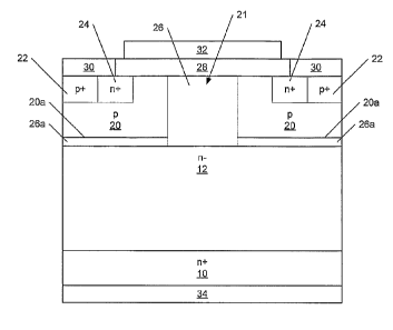
Figure 1 is a cross-sectional view of a conventional DIMOSFET;
Figure 2A is a cross-sectional view of a SiC MOSFET according to
embodiments of the present invention;
Figure 2B is a cross-sectional view of a SiC MOSFET according to
embodiments of the present invention;
Figure 3 is a cross-sectional view of a SiC MOSFET according to further
embodiments of the present invention;
Figures 4A through 4H illustrate processing steps in the fabrication of
MOSFETS according to various embodiments of the present invention;
Figures SA through 5D illustrate processing steps in the fabrication of
MOSFETS according to further embodiments of the present invention;
Figures 6A and 6B are simulation results for a conventional DIMOSFET
illustrating on-state resistance and oxide field voltage versus gap between
the p-well
regions of the simulated device;
7
CA 02502850 2005-04-20
WO 2004/061974 PCT/US2003/038490
Figures 7A and 7B are simulation results for a DIMOSFET with a implanted
spacer illustrating on-state resistance and oxide field voltage versus gap
between the
p-well regions of the simulated device;
Figures 8A and 8B are simulation results for a DIMOSFET according to
embodiments of the present invention illustrating on-state resistance and
oxide field
voltage versus gap between the p-well regions of the simulated device;
Figures 9A and 9B are experimentally obtained I-V curves for a DIMOSFET
with a implanted spacer (Figure 9A) and a DIMOSFET according to embodiments of
the present invention (Figure 9B); and
Figures l0A and lOB axe experimentally obtained reverse bias leakage curren
plots for a DIMOSFET with a implanted spacer (Figure l0A) and a DIMOSFET
according to embodiments of the present invention (Figure lOB).
Detailed Description of the Invention
The present invention now will be described more fully hereinafter with
reference to the accompanying drawings, in which preferred embodiments of the
invention are shown. This invention may, however, be embodied in many
different
forms and should not be construed as limited to the embodiments set forth
herein;
rather, these embodiments are provided so that this disclosure will be
thorough and
complete, and will fully convey the scope of the invention to those skilled in
the art.
As illustrated in the Figures, the sizes of layers or regions axe exaggerated
for
illustrative purposes and, thus, are provided to illustrate the general
structures of the
present invention. Like numbers refer to like elements throughout. It will be
understood that when an element such as a layer, region or substrate is
referred to as
being "on" another element, it can be directly on the other element or
intervening
elements may also be present. In contrast, when an element is referred to as
being
"directly on" another element, there are no intervening elements present.
Embodiments of the present invention provide silicon carbide MOSFETs
and/or methods of fabricating silicon carbide MOSFETs which may reduce on-
state
resistance of a device. While the inventors do not wish to be bound by any
theory of
operation, it is believed that by reducing the depletion region beneath the p-
well of
the MOSFET, the length of the current path may be reduced and, therefore, the
on-
state resistance of the device may be reduced over that of a similarly sized
CA 02502850 2005-04-20
WO 2004/061974 PCT/US2003/038490
conventional MOSFET. Furthermore, by reducing the depletion region in the JFET
gap, device areas may be reduced by reducing the size of the JFET gap.
MOSFETs according to embodiments of the present invention are illustrated
in Figure 2A. As seen in Figure 2A, in particular embodiments of the present
invention, a lightly doped ri drift layer 12 of silicon carbide is on an
optional n+ layer
of silicon carbide. The ri drift layer 12 may be a substrate or an epitaxial
layer of
silicon carbide and may, for example, be 4H polytype silicon carbide. In
certain
embodiments, the ri drift layer 12 has a carrier concentration of from about
1014 to
about S X 1 O16 Cm 3. Furthermore, in some embodiments of the present
invention, the
10 drift layer 12 has a thickness of from about 5 ~m to about 150 Vim.
Furthermore, the
n+ layer 10 may be an implanted layer or region, an epitaxial layer or a
substrate. In
some embodiments, the ri layer has a carrier concentration of from about 1018
to
about 1021 cm 3.
A region of higher carrier concentration n-type silicon carbide 26 is provided
on the drift layer 12. The region 26 has a higher carrier concentration than
the carrier
concentration of the drift layer 12 and provides an embodiment of a JFET
limiting
region 26a between a floor 20a of the p-wells 20 and the drift layer 12. The
region 26
may be provided by epitaxial growth or by implantation. In certain embodiments
of
the present invention, the region 26 has thickness of from about 0.5 ~m to
about 1.5
~,m. Also, the region 26 may have a carrier concentration of from about 1015
to about
5 X 101' cm 3. The region 26 may have a uniform carrier concentration or a non-
uniform carrier concentration.
As is further seen in Figure 2A, spaced apart regions of p-type silicon
carbide
provide p-wells 20 in the region 26. The p-wells 20 are implanted so as to
extend into
but not through the region 26 such that a region of higher carrier
concentration n-type
silicon carbide 26a is provided between a floor 20a of the p-wells 20 and the
drift
layer 12. In particular embodiments, the portion of the region 26 in the gap
21
between the p-wells 20 has a higher carrier concentration than the drift layer
12. In
other embodiments of the present invention, the portion of the region 26 in
the gap 21
between the p-wells 20 has the same carrier concentration as the drift layer
12. Thus,
the portion of the region 26 adjacent the sidewalls of the p-wells 20 may have
the
same or higher carrier concentration than the drift layer 12 while the portion
26a of
the region 26 adjacent the floor 20a of the p-wells 20 has a higher carrier
concentration than the drift layer 12. In particular embodiments, the p-wells
20 have
9
CA 02502850 2005-04-20
WO 2004/061974 PCT/US2003/038490
a carrier concentration of from about 1016 to about 1019 cm 3. Furthermore,
the p-
wells 20 may provide a junction depth of from about 0.3 ~m to about 1.2 Vim.
An example of embodiments of the present invention where the gap 21 and the
area beneath the p-wells 20 have different carrier concentrations is
illustrated in
Figure 2B. As seen in Figure 2B, regions 26' are provided beneath the floor of
the p-
wells 20 and between the p-wells 20 and the drift layer 12 to provide the JFET
limiting regions. However, the drift layer 12 is provided in the gap 21
between the p-
wells 20. The regions 26' may be provided, for example, by implanting n-type
regions 26' in the drift layer 12 using a mask and implanting the p-wells 20
so that the
depth of the p-wells 20 in the drift layer 12 is less than the greatest depth
of the
regions 26' in the drift layer 12. Similarly, an n-well could be formed in the
drift
layer 12 and the p-wells 20 formed in the n-well.
In some embodiments, the p-wells 20 are implanted with A1 and annealed at a
temperature of at least about 1500°C. However, other suitable p-type
dopant may be
utilized in providing the p-wells 20. The doping profile of the p-wells 20 may
be a
substantially uniform profile, a retrograde profile (increasing doping with
depth) or
the p-wells may be totally buried (with some n-type silicon carbide above the
p-wells
20). In some embodiments, the p-wells 20 may have carrier concentrations of
from
about 1x10¹⁶ to about 1x1019 cm 3 and may extend into the region 26 or the ri
drift
layer 12 from about 0.3 ~m to about 1.2 ~,m. While various p-type dopants may
be
utilized, A1 is utilized in some embodiments because Boron tends to diffuse
over
several microns when annealed at temperatures exceeding 1500°C.
Therefore, it may
be difficult to control the precise gap between the p-wells 20 (the region
which may
be referred to as the JFET region 21) and/or the depth of the p-wells 20. If
this gap is
too high, the field in the gate oxide can become too high when the device is
in the
blocking state. However, if the gap is too narrow, the resistance of the JFET
region
21 may become very high. Accordingly, gaps of from about 1 ~m to about 10 ~,m
axe
preferred. The particular gap utilized for a given device may depend upon the
desired
blocking voltage and on-state resistance of the device.
Regions of ri silicon carbide 24 and, optionally, regions of p+ silicon
carbide
22 are disposed within the p-wells 20. In some embodiments, the regions of n+
silicon
carbide 24 are spaced from about 0.5 ~,m to about 5 ~,m from the edge of the p-
wells
20 adjacent the JFET region 21. The regions of n+ silicon carbide 24 may have
a
CA 02502850 2005-04-20
WO 2004/061974 PCT/US2003/038490
doping concentration of from about 5 X 1018 cm 3 to about 1021 cm 3 and may
extend
to a depth of from about 0.1 ~,m to about 0.8 ~m into the p-wells 20 but are
shallower
than the depth of the p-wells 20. Suitable n-type dopants include phosphorous
and
nitrogen or other n-type dopants known to those of skill in the art. The
optional
regions of p+ silicon carbide 22 may be adjacent the regions of ri silicon
carbide 24
and opposite the edge of the p-wells 20. The regions of p+ silicon carbide 22
may
have a doping concentration of from about 5 X 1018 cm 3 to about 1021 cm 3 and
may
extend to a depth of from about 0.2 ~m to about 1.2 ~,m into the p-wells 20
but are
shallower than the depth of the p-wells 20.
The gate oxide 28 extends at least between the n+ regions of silicon carbide
24
and has a gate contact 32 thereon. In some embodiments, the gate oxide 28 may
be
either a thermally grown oxide with an NO or N20 anneal or Oxide/Nitride/Oxide
(ONO) where the first oxide is a thermal oxide followed by an NO or N20
anneal.
The gate contact material may be any suitable contact material. In some
embodiments, the gate contact material is molybdenum or p-type polysilicon. P-
type
polysilicon may be suitable in some embodiments because of its high work
function.
The thickness of the gate oxide 28 may depend on the work function of the
material of
the gate contact 32. However, in general, thicknesses of from about 100 A to
about
5000 A are preferred.
One or more source contacts 30 and a drain contact 34 are also provided.
Source contacts 30, in some embodiments are formed of nickel (Ni), titanium
(Ti),
platinum (Pt) or aluminum (Al), combinations thereof and/or other suitable
contact
materials and may be annealed at temperatures of from about 600 °C to
about 1000
°C, for example, 825 °C, so as to provide an ohmic contact to
both the p+ regions 22
and the n+ regions 24. The drain contact 34 may be Ni or Ti or other such
suitable
material for forming an ohmic contact to n-type silicon carbide.
Differing or the same contact materials may be utilized to contact the p+
regions 22 and the n+ regions 24. Furthermore, while not illustrated in the
Figures,
one or more metal overlayers may be provided on one or more of the contacts.
Techniques and materials for providing metal overlayers are known to those of
skill in
the art and, therefore, are not discussed further herein.
Figure 3 illustrates further alternative embodiments of the present invention
which utilize a re-grown epitaxial layer. As seen in Figure 3, a thin layer of
silicon
carbide 27 is re-grown on the p-wells 20 after implanting and annealing the p-
wells
11
CA 02502850 2005-04-20
WO 2004/061974 PCT/US2003/038490
and extends across the region 26 in the JFET region. Embodiments such as
illustrated
in Figure 2B may also be modified to include such a re-grown epitaxial layer
that is
re-grown on the p-wells 20 after implanting and annealing the p-wells and
extends
across the drift layer 12 in the JFET region. The n+ regions of silicon
carbide 24 may
be formed through the re-grown silicon carbide layer 27 and/or prior to re-
growth.
The re-grown silicon caxbide layer 27 may have a thickness of from about 0.05
~.m to
about 1 ~,m in come embodiments. The re-grown silicon carbide layer 27 may be
n-
type silicon carbide. In certain embodiments, the re-grown silicon carbide
layer 27
has a doping of from about 5 X 1014 cm 3 to about 5 X 101' cm 3.
As is further seen in Figure 3, because of the regrown silicon carbide layer
27,
a contact window is provided through the silicon carbide layer 27 to provide a
contact
30' to the optional p+ regions 22 or to the p-wells 20 if the p+ regions 22
are not
present. The contact 30' may be made of any suitable material for forming an
ohmic
contact as described above.
While Figures 2A, 2B and 3 illustrate embodiments of the present invention
as discrete devices, as will be appreciated by those of skill in the art,
Figures 2A, 2B
and 3 may be considered unit cells of devices having multiple cells. Thus, for
example, additional unit cells may be incorporated into the devices
illustrated in
Figures 2A, 2B and 3 by dividing the device along its central axis
(illustrated as the
vertical axis in Figures 2A, 2B and 3) and rotating the divided device about
an axis of
the periphery of the devices illustrated in Figures 2A, 2B and 3 (the vertical
edges of
the devices illustrated in Figures 2A, 2B and 3). Accordingly, embodiments of
the
present invention include devices such as those illustrated in Figures 2A, 2B
and 3 as
well as devices having a plurality of unit cells incorporating the JFET
limiting regions
illustrated in Figures 2A, 2B and 3.
Fabrication of devices according to embodiments of the present invention
having a JFET limiting region provided by an epitaxial layer will now be
described
with reference to Figures 4A through 4I3 and SA through SD. As will be
appreciated
by those of skill in the art in light of the present disclosure, embodiments
of the
present invention having a JFET limiting region provided by implantation may
be
provided by modifying the operations described herein to provide such
implanted
regions as described above.
As seen in Figure 4A, an n-type silicon carbide epitaxial layer 26 is formed
on
the drift layer 12. The n-type epitaxial layer 26 may be formed to the
thickness and
12
CA 02502850 2005-04-20
WO 2004/061974 PCT/US2003/038490
doping levels described above. As seen in Figure 4S, a mask 100 is formed and
patterned on the n-type epitaxial layer 26 and impurities are implanted into
the n-type
epitaxial layer 26 to provide the p-wells 20. The implanted impurities may be
implanted to the depths described above and to provide the desired carrier
concentrations when activated. Alternatively, the drift layer 12 may be
provided on
an n+ silicon carbide substrate. In such embodiments, the n+ layer described
below
may be provided by the substrate.
As is seen in Figure 4C, the mask 100 is removed and a mask 104 is formed
and patterned and n-type impurities are implanted utilizing the mask 104 to
provide
the n~ regions 24. The mask 104 is formed to provide the desired spacing
between the
periphery of the p-wells 20 and the ri regions 24 that defines the channel
length of the
shorting channels 26. Suitable n-type impurities include nitrogen and
phosphorous.
Furthermore, the impurities may be implanted to provide the dimensions and
carrier
concentrations of the n+ regions 24 described herein.
Figure 4D illustrates the formation of the optional p+ regions. The mask 104
is removed and a mask 106 is formed and patterned and p-type impurities are
implanted utilizing the mask 106 to provide the p+ regions 22. The p-type
impurities
may be implanted to provide the dimensions and carrier concentrations of the
p+
regions 22 described herein. In some embodiments, the p-type impurity is
aluminum,
however, other suitable p-type impurities may also be utilized.
Figure 4E illustrates the removal of the mask 106 as well as the creation of
the n+ layer 10, which may be formed by a backside implant of n-type
impurities in a
substrate or may be an epitaxial layer or the substrate itself and may be
formed prior
to Figure 4A. The structure is also annealed at a temperature of from about
1200 °C
to about 1800 °C for durations from about 30 seconds to about 24 hours
to activate the
implanted p-type and n-type impurities. Optionally, the structure may be
capped with
a dielectric layer, such as Si02 or Si3N4, to protection the structure during
annealing.
Alternatively, in embodiments where the gate oxide is annealed after formation
to
improve the SiC/Si02 interface, the activation of such impurities may be
provided by
such anneal.
Figure 4F illustrates the formation of the gate oxide 28. The gate oxide may
be thermally grown and may be a nitrided oxide andlor may be other oxides. The
nitrided oxide may be any suitable gate oxide, however, in certain
embodiments,
SiOa, oxynitride or ONO are utilized. Formation of the gate oxide or the
initial oxide
13
CA 02502850 2005-04-20
WO 2004/061974 PCT/US2003/038490
of an ONO gate dielectric may be followed by an anneal in N20 or NO so as to
reduce
defect density at the SiC/oxide interface. In particular embodiments, the gate
oxide is
formed either by thermal growth or deposition and then annealed in an N20
environment at a temperature of greater than about 1100 °C and flow
rates of from
about 2 to about 8 SLM which may provide initial residence times of the NZO of
from
about 11 to about 45 seconds. Such formation and annealing of an oxide layer
on
silicon carbide are described in commonly assigned United States Patent
Application
Serial No. 09/834,283, entitled "Method of N20 Annealing an Oxide Layer on a
Silicon Carbide Layer", United States Provisional Application Serial No.
60/237,822
entitled "Method of N20 Growth of an oxide layer on a Silicon Carbide Layer"
filed
May 30, 2001, United States Patent Application Serial No. 09/968,391 entitled
"Method Of NO Growth Of An Oxide On A Silicon Carbide Layer" filed October l,
2001, and/or United States Patent Application Serial No. 10/045,542 entitled
"Method
Of Fabricating an Oxide Layer on a Silicon Carbide Layer Utilizing an Anneal
in a
Hydrogen Environment" filed October 26, 2001, the disclosures of which are
incorporated herein by reference as if set forth fully herein.
Additionally, an NZO grown oxide may also be utilized as described in J. P.
Xu, P. T. Lai, C. L. Chars, B. Li, and Y. C. Cheng, "Improved Performance and
Reliability of N20-Grown Oxynitride on 6H-SiC," IEEE Electron Device Letters,
Vol. 21, No. 6, pp. 298-300, June 2000. Techniques as described in L. A.
Lipkin and
J. W. Palmour, "Low interface state density oxides on p-type SiC," Materials
Science
Forum Vols. 264-268, pp. 853-856, 1998 may also be utilized. Alternatively,
for
thermally grown oxides, a subsequent NO anneal of the thermally grown Si02
layer
may be provided to reduce the interface trap density as is described in M. K.
Das, L.
A. Lipkin, J. W. Palmour, G. Y. Chung, J. R. Williams, K. McDonald, and L. C.
Feldman, "High Mobility 4H-SiC Inversion Mode MOSFETs Using Thermally
Grown, NO Annealed Si02," IEEE Device Research Conference, Denver, CO, June
19-21, 2000; G. Y. Chung, C. C. Tin, J. R. Williams, K. McDonald, R. A.
Weller, S.
T. Pantelides, L. C. Feldman, M. K. Das, and J. W. Palmour, "Improved
Inversion
Channel Mobility for 4H-SiC MOSFETs Following High Temperature Anneals in
Nitric Oxide," IEEE Electron Device Letters accepted for publication; and G.
Y.
Chung, C. C. Tin, J. R. Williams, K. McDonald, M. Di Ventra, S. T. Pantelides,
L. C.
Feldman, and R. A. Weller, "Effect of nitric oxide annealing on the interface
trap
densities near the band edges in the 4H polytype of silicon carbide," Applied
Physics
14
CA 02502850 2005-04-20
WO 2004/061974 PCT/US2003/038490
Letters, Vol. 76, No. 13, pp. 1713-1715, March 2000. Oxynitrides may be
provided
as described in United States Patent Application Serial No. 09/878,442,
entitled "High
Voltage, High Temperature Capacitor Structures and Methods of Fabrication"
filed
Jme 11, 2001, the disclosure of which is incorporated herein by reference as
if set
forth fully herein.
Figure 4G illustrates formation of the gate contact 32. As described above,
the gate contact 32 may be p-type polysilicon and/or may be other suitable
contact
material and may be formed and patterned utilizing techniques known to those
of skill
in the art. Alternatively, the oxide 28 of Figure 4F and the gate contact 32
may be
formed and patterned together. Finally, Figure 4H illustrates formation of the
source
and drain contacts 30 and 34 respectively, that may be formed by evaporative
deposition, sputtering or other such techniques known to those of skill in the
art. In
certain embodiments, the source and drain contacts 30 and 34 are nickel which
is
annealed at about 825 °C after formation so as to improve the quality
of the olunic
contact.
Figures SA through SD illustrate operations in the fabrication of devices
according to alternative embodiments of the present invention utilizing a
regrown
epitaxial layer. Operations for fabrication of the devices are the same as
those
described above with reference to Figures 4A through 4E and continue with the
operations illustrated in Figure SA. As seen in Figure 5A, an n-type epitaxial
layer
27 is formed on the structure of Figure 4E. Such growth may be provided before
or
after annealing to activate the implants. The epitaxial layer 27 is patterned
to extend
between the implanted regions 24 as seen in Figure SB. Figure 5B also
illustrates the
formation of the gate oxide 28. In some embodiments, the gate oxide 28 is
thermally
grown and may be a nitrided oxide. The nitrided oxide may be any suitable gate
oxide, however, Si02, oxynitride or ONO may be prefeiTed. Formation of the
gate
oxide may be carried out as described above with reference to Figure 4F.
Figure SC illustrates formation of source contacts 30'. As seen in Figure SC,
windows are opened in the gate oxide 28 corresponding to the location of the
p+
regions 22 and/or n+ regions 24. The contacts 30' are then formed in the
window.
Figure SD illustrates formation of the gate contact 32 and the source contacts
30'.
Alternatively, the oxide 28 of Figure SD and the gate contact 32 may be formed
together. Thus, the gate contact may be formed and patterned prior to opening
windows for the source contacts. As described above, the gate contact 32 may
be p-
CA 02502850 2005-04-20
WO 2004/061974 PCT/US2003/038490
type polysilicon or may be other suitable contact material and may be formed
and
patterned utilizing techniques known to those of skill in the art. Source
contacts 30'
may be formed by evaporative deposition, sputtering or other such techniques
known
to those of skill in the art. Finally, Figure SD also illustrates formation of
the drain
contact 34 which may be formed by evaporative deposition, sputtering or other
such
techniques known to those of skill in the art. In certain embodiments, the
source and
drain contacts 30' and 34 are nickel which is annealed at temperature of from
about
600 °C to about 1000 °C, for example, about 825 °C, after
formation so as to improve
the quality of the ohmic contact.
In addition to the embodiments described herein, embodiments of the JFET
limiting regions may also be provided in DMOSFETs as described in United
States
Patent Application Serial No. 09/911,995 filed July 24, 2001 and entitled
"Silicon
Carbide Power Metal-Oxide Semiconductor Field EfFect Transistors Having a
Shorting Channel and Methods of Fabricating Silicon Carbide Metal-Oxide
Semiconductor Field Effect Transistors Having a Shorting Channel," the
disclosure of
which is incorporated herein as if set forth fully.
While embodiments of the present invention have been described with
reference to particular sequences of operations, as will be appreciated by
those of skill
in the art, certain operations within the sequence may be reordered while
still
benefiting from the teachings of the present invention. For example, in
particular
embodiments of the present invention, the formation of the n+ regions 24 and
the p+
regions 22 may be reversed. Accordingly, the present invention should not be
construed as limited to the exact sequence of operations described herein.
Figures 6A through 8B are 2D simulation results for various DMOSFET
structures illustrating on-state resistance or oxide field strength versus
JFET gap
distance. Figures 6A and 6B are simulation results for a conventional DMOSFET
having a 6 X 10¹⁴ crri 3 and 115 ~,m thick drift layer and 10 ~m wide p-wells
that
extend 0.75 ~.m into the drift layer. Figures 7A and 7B are simulation results
for a
DMOSFET having a 6 X 1014 cm 3 and 115 ~,m thick drift layer, 10 ~,m wide p-
wells
that extend 0.75 ~.m into the drift layer and a 5 X lOls cm 3 spacer implant
that
extends 0.75 ~,m into the drift layer. Figures 8A and 8B are simulation
results for a
DMOSFET according to embodiments of the present invention having a 6 X 1014 cm
3
and 115 ~m thick drift layer, 10 ~,m wide p-wells that extend 0.75 ~,m into a
5 X l Ols
cm 3 epitaxial layer that is 1.75 ~m thick. As seen in Figures 6A through 8B,
16
CA 02502850 2005-04-20
WO 2004/061974 PCT/US2003/038490
embodiments of the present invention may provide narrower JFET gaps for a
given
maximum oxide field as well as reduced on state resistance.
Figure 9A is a measured I-V curve for a DMOSFET without the JFET
limiting region according to embodiments of the present invention and Figure
9B is a
measured I-V curve for a DMOSFET with JFET limiting regions according to
embodiments of the present invention. As seen in Figures 9A and 9B, the
measured
on-state resistance is reduced from 266 mSZ-cm2 to 189 mS2,-cm2. Furthermore,
Figure l0A is a measured drain leakage current trace for a DMOSFET without the
JFET limiting region according to embodiments of the present invention and
Figure
lOB is a measured drain leakage trace for a DMOSFET with JFET limiting regions
according to embodiments of the present invention. As seen in Figures l0A and
lOB,
both devices had a breakdown voltage of greater than 3150 V.
In the drawings and specification, there have been disclosed typical preferred
embodiments of the invention and, although specific terms are employed, they
are
used in a generic and descriptive sense only and not for purposes of
limitation.
17