Note: Descriptions are shown in the official language in which they were submitted.
CA 02503055 2005-04-19
WO 2004/040822 PCT/US2003/033708
RADIO RECEIVER AND METHOD FOR AM SUPPRESSION
AND DC~OFFSET REMOVAL
1. Field of the Invention
This invention generally relates to signal-processing systems, and more
particularly to a system and method for recovering a baseband signal in a
receiver of a
communications system.
2. Backgiround of the Related Art
The design of a radio transceiver having a small form factor and which can be
manufactured at low cost is highly desirable for use in modern wireless
communication
systems, and this is especially true in cellular systems. However, a fully
integrated radio
transceiver design is difficult to implement because many cellular standards
have severe
performance demands in terms of sensitivity and selectivity.
The direct-conversion radio transceiver architecture is thought to be an ideal
solution for replacing the widely-used superheterodyne architecture. The
difficulty in design
is much more severe in the receiver side than in the transmitter side because
the selectivity
and sensitivity requirements should be met at the same time in receiver.
Figure 1 shows a related art superheterodyne radio receiver architecture, and
Figure 2 shows a related art direct-conversion radio receiver architecture.
One difference between these architectures is that the superheterodyne
architecture performs channel selection and amplification at some specified
IF(Intermediate
Frequency). Even though one or more external channel selection filters are
usually formed
by ceramic filters or SAW filters, performing channel selection at IF is
advantageous in at
least the following respects.
First, DC-offset is not an issue because simple AC coupling can reject the
generation of DC offset and enable fast settling. Also, a 11f noise problem
found in related
art direct conversion radio receiver is minimized because the amplification is
performed at
an IF frequency which is far from DC. Second, strong blockers and adjacent
channel
signals are mostly filtered by almost-ideal passive filters. Thus, the concern
for linearity is
relaxed.
The direct-conversion radio receiver architecture should solve and address the
aforementioned problems in the related art. Unlike the superheterodyne
receiver, DC-
offset is an issue in a direct conversion receiver and thus adequate DC-offset
removal
circuitry should be employed. Even though such DC-offset removal circuitry
works, there
are numerous drawbacks in real world applications.
i
CA 02503055 2005-04-19
WO 2004/040822 PCT/US2003/033708
First, the cut-off frequency of a DC-offset cancelling loop should be
sufficiently
smaller than the desired signal bandwidth to reduce the effect of inter-symbol
interference.
Normally, the cut-off frequency of the DC-offset cancelling loop is set to
111000 of channel
bandwidth. Even though techniques have been proposed which can render this DC
servo
loop with a small die size, the design of circuit parameters may not be
realistic, in the case
of very small channel bandwidth like those used in GSM and PDC communication
networks.
In the GSM standard, the channel spacing is 200KHz and only 25KHz in PDC.
Even worse, the GMSK signal used in GSM standard has most of the signal energy
at DC
when down-converted to DC. Thus, DC-offset cancellation becomes harder to
perform in
GSM applications. The DC-offset cancellation loop can reject the static DC-
offset, but a
long transient is found when the dynamic DC-offset arises. The settling time
is inversely
proportional to the cut-off frequency and thus may not acceptable for some
applications.
Especially, to satisfy all the requirements of GSM, the radio receiver should
be
designed to pass a single-tone blocking test and AM suppression test. Although
the signal
power is larger in case of single tone blocker, the built-in DC-offset removal
circuit can
easily filter out the DC-offset caused by the second-order distortion from the
strong blocker
signal, because the block signal is assumed to be continuous sine-wave signal.
However,
in the AM suppression test, the strong blocking signal arrives the middle of
packet and thus
the DC-offset caused by this blocker cannot be filtered out so fast and last
for a long time
for settling.
Also in GSM applications, one-time DC-offset cancellation is usually employed
due
to the packet-based signal transmission. In this case, the DC-offset will
degrade the signal-
to-noise ratio at the base-band output if it is not properly filtered at the
digital base-band
modem. Modern GMSK demodulators incorporate the high-performance analog-to-
digital
converter prior the digital signal processing. Although use of the analog-to-
digital converter
with high dynamic range and additional DC-offset correction method in DSP can
solve this
problem, it still puts the design difficulty for analog-to-digital converter
and the DC-offset
should not exceed the dynamic range of the analog-to-digital converter.
One method which has been proposed to solve the DC-offset problem and AM
suppression is to use the analog-to-digital converter with high dynamic range
and to adopt
a DC-offset cancellation algorithm running in a digital signal processor. In
this case, the
amount of DC-offset should be small enough not to exceed the full dynamic
range of the
analog-to-digital converter. Typically, most of the channel selection and gain
control is
2
CA 02503055 2005-04-19
WO 2004/040822 PCT/US2003/033708
performed in a base-band modem, not in the analog part of the receiver. The
design
challenge lies in the design of a high-performance analog-to-digital
converter.
Another method which has been proposed to solve the DC-offset problem or
second-order distortion is to use a very low-IF architecture rather than a
direct-conversion
architecture. In a very low-IF architecture, the DC-offset caused by the
second-order
distortion lies outside the signal band and thus is easily removed by digital
filtering. The
requirement for IIP2 indicating the amount of the second-order distortion is
relaxed by the
amount of filtering in the low-IF receiver. However, digital filtering also
requires a large
number of bits in analog-to-digital converter and may not acceptable for its
high-current
consumption. Thus, use of digital low-IF radio receiver architecture is
limited to applications
such as GSM.
The above references are incorporated by reference herein where appropriate
for
appropriate teachings of additional or alternative details, features andlor
technical
background.
SUMMARY OF THE INVENTION
An object of the invention is to solve at least the above problems andlor
disadvantages and to provide at least the advantages described hereinafter.
The present invention is a receiver including a baseband signal recovery
circuit
which uses a low-IF architecture for data reception. The receiver preferably
uses a full-
analog implementation for channel selection and filtering. Thus, the overhead
placed on
the design of analog-to-digital converter is greatly relaxed and most of
hardware can be re-
used for multi-mode applications with only a slight modification. The present
invention is
suitable for use in applications requiring highly integrated radio receiver
architectures.
Additional advantages, objects, and features of the invention will be set
forth in
part in the description which follows and in part will become apparent to
those having
ordinary skill in the art upon examination of the following or may be learned
from practice of
the invention. The objects and advantages of the invention may be realized and
attained
as particularly pointed out in the appended claims.
BRIEF DESCRIPTION OF THE DRAWINGS
The invention will be described in detail with reference to the following
drawings in
which like reference numerals refer to like elements wherein:
Figure 1 is a block diagram showing a related art superheterodyne radio
receiver;
3
CA 02503055 2005-04-19
WO 2004/040822 PCT/US2003/033708
Figure 2 is a block diagram showing a related art direct conversion radio
receiver;
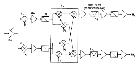
Figure 3 is a block diagram of a radio receiver in accordance with an
exemplary
embodiment of the present invention;
Figure 4 is a diagram showing a transfer function of an elliptic filter in
accordance
with an exemplary embodiment of the present invention;
Figure 5 is a diagram showing waveforms produced at various stages of a radio
receiver implemented in accordance with an exemplary embodiment of the present
invention;
Figure 6 is a block diagram showing a DDFS circuit for generating an
oscillator
signal which may correspond to the second local oscillator (LO) signal of the
present
invention; and
Figure 7 is a block diagram showing another circuit for generating an
oscillator
signal which may correspond to the second local oscillator (LO) signal of the
present
invention.
DETAILED DESCRIPTION OF PREFERRED EMBODIMENTS
Figure 3 shows a baseband signal recovery circuit in accordance with one
exemplary embodiment of the present invention. Instead of the related art's
direct-
conversion radio architecture, the present invention uses a low-IF
architecture for data
reception. However, unlike other related art systems, at least one embodiment
of the
present invention uses a full-analog implementation for channel selection and
filtering.
Thus, the overhead placed on the design of analog-to-digital converter is
greatly relaxed
and most of hardware can be re-used for multi-mode applications with only a
slight
modification.
As shown in Figure 3, an RF front-end mixer down-converts an RF signal from
LNA 1 into respective intermediate frequency I and Q signals using a
quadrature mixer,
which includes mixers 2 and 3. The quadrature mixer should have well-matched
phase and
gain in IIQ signal for sufficient image rejection. By virtue of weak adjacent
channel signal
power in GSM standard, the required amount of image rejection will be around
40dB.
After the first down-conversion stage, an optional gain stage and filtering
stage
may be employed to partially reject strong out-of band signals and to block
noise from
propagating into the following stages.
The second down-conversion mixer 4 converts the low-IF signal into a base-band
signal. After performing this second-down conversion, an optional gain stage
may also be
4
CA 02503055 2005-04-19
WO 2004/040822 PCT/US2003/033708
implemented to block noise from being input into the following stage. The
residual DC-
offset signal or induced dynamic DC-offset from the second-order distortion
undergoes
frequency translation via the second mixer, and the frequency becomes the same
as the
frequency of the second LO signal.
After the second-down conversion, a notch-filter 5 with a deep notch at the
same
frequency as that of the second LO signal is present to suppress this unwanted
signal.
Although a low-pass filter may be used to reject the unwanted signal, the
notch filter is
much more suitable for eliminating the single-tone signal caused by static or
dynamic DC-
offset. The notch filter may be implemented by an elliptic filter andlor a
chebyschef II type
which has zero at some desired frequency. Unlike a DC servo loop, the response
time of
the present offset canceling circuitry is quite fast, because the DC-offset is
translated into
the high frequency rather than being located at DC. Thus, adverse effects from
the DC-
offset is greatly relaxed both in its absolute value and the correction time.
The design of
the second LO frequency is important in the present invention in terms of
image rejection
and capability of AM suppression. When the low IF architecture is used, some
amount of
signal leakage from the in-band blocking signal to the desired band is
inevitable, due to the
gain and phase imbalance in the first LO signal and first LO mixer (2 and 3 in
Figure 3).
For example, when the second LO signal is 100KHz in a GSM application, the
desired signal will be centered at 100KHz. The in-band blocking signal located
below
400KHz from the desired signal will have some image component at 300KHz. Since
the in
band blocking signal at that frequency has the higher magnitude by more than
40dB
compared with the desired signal, the image rejection from the first mixer
should be better
than 36dB to get the desired SNR. When the second LO signal moves toward
higher
frequency, the requirement in image rejection becomes much more severe because
of
higher blocking signal level. Thus, it is desirable to locate the second LO
frequency as low
as possible to relax the image requirement given to the first mixer. However,
the transient
response of the notch filter depends on the location of the notch, and the
settling time is
inversely proportional to the frequency. The DC offset caused by the strong
blocking signal
in a GSM application undergoes the frequency translation with the second
mixer(4 in
Figure 3), becoming to the carrier leakage. This carrier leakage is
proportional to the
amount of the DC offset and the frequency is the same as the second LO signal.
This
carrier leakage should be removed quickly to avoid causing the bit error
during the
demodulation process in the base-band modem. Since the bit error happens in
case that
the transient time of the DC offset removal with the help of the notch filter
is quite long, the
5
CA 02503055 2005-04-19
WO 2004/040822 PCT/US2003/033708
location of the notch should be as high as possible. When considering both
requirement of
image rejection and transient response, the second LO frequency is usually
determined
close to 100KHz.
Figure 4 is a diagram showing one example of a transfer function of an
elliptic filter
with a zero at a designed position. As shown in Figure 4, the notch is caused
by a zero in
the filter transfer function. The zero in the filter transfer function means
the gain at the
particular signal frequency and thus can be suppressed sufficiently. When
considering the
particular example of a GSM receiver, the requirement for the second order-
distortion is
calculated as follows.
Consider the case where the input blocking signal has a power of -3ldBm at
6MHz frequency offset from the desired signal and the desired signal has -
99dBm which is
3dB above from the sensitivity level. To maintain 9dB of SNR, the IIP2 at the
input of LNA
should be greater than
2 x (-31) - (-99) + 9 = 46 dBm (1)
Assuming the gain of the LNA to be 15dB, the first down-conversion mixer
should
have IIP2 performance better than 61dBm. This value is not readily achievable
by other
circuit design techniques that are used in the related art. However, in the
two-step down
conversion architecture of the claimed embodiments of the present invention,
assuming
that the notch filter suppresses the signal by 30dB at the zero location, IIP2
performance
can be relaxed by a same amount. The resulting requirement of IIP2 for the
mixer is about
16dBm, which is readily achievable.
Figure 5 shows various exemplary operating waveforms which may be produced at
various stages of a receiver constructed in accordance with one exemplary
embodiment of
the present invention. As shown, when a strong blocking signal arrives at the
input of LNA
1, some amount of DC-offset is produced especially in the first down-
conversion mixer.
Even though the low-pass filter after the first down-conversion mixer
suppresses this
blocking signal, DC-offset is produced due to second-order distortion. The IF
signal is
greater than the signal bandwidth and thus the DC-offset itself lies outside
the desired
signal.
After second-down conversion, the desired signal is centered at DC and DC-
offset
becomes a single-tone signal at the second LO frequency. The notch filter
suppresses this
single-tone signal to a negligible or acceptable level. Also, after the second
down-
6
CA 02503055 2005-04-19
WO 2004/040822 PCT/US2003/033708
conversion, the optional gain stages and filtering stages reject remaining
interferers to
provide the desired signal and meet the signal strength for the analog-to-
digital converter.
In implementing the exemplary embodiments of the present invention, it is
preferable for the second LO signal to be designed with a spectral purity in
order to realize
an acceptable signal-to-noise ratio (SNR). The harmonics of the second LO
signal should
be suppressed sufficiently, so as not to produce severe interference problems
by harmonic
mixing or spurious mixing. Also, it is preferable for the frequency of the LO
signal to be
exactly like the frequency of the first LO signal.
In accordance with one exemplary embodiment, the LO signals may be generated
using a Phase Locked Loop (PLL) circuit. However, the frequency of the second
LO signal
may be too low in some circumstances, and when this condition does exist, it
is quite
ineffective to use a PLL for second LO generation.
Thus, in accordance with another exemplary embodiment, the present invention
generates the second local oscillator (LO) frequency in one of two ways. The
first way
involves using Direct Digital Frequency Synthesizer (DDFS) for the generation
of the
second LO signal. One example of a DDFS technique suitable for use with the
present
nvention is disclosed at the website www.analog.com.
Figure 6 shows a general block diagram of a circuit implementing a DDFS
technique. In this diagram, the ROM table and DACs are clocked by the
reference clock
input, and the circuit generates a pure single-tone for the second LO signal.
Depending on
the size of ROM and bits of DAC, spectral purity in this example reaches less
than -90dBc.
In Figure 6, the sin lookup table contains sine data for an integral number of
cycles. Those
skilled in the art will appreciate that other transcendental function data can
be used in the
lookup table without departing from the spirit and scope of the present
invention.
The second way involves using a divided reference clock input with post
filtering to
reject harmonic signals. Figure 7 shows an exemplary circuit which generates
an LO
frequency signal based on this approach. When implemented in a GSM
application, for
example, the entire system uses 13MHz or 26MHz as the reference clock signal
source
from an external crystal oscillator. When divided by 100 or 200 times, the
second LO signal
becomes 130KHz. The divide-by-4 circuit provides the exact quadrature signal
for single-
sided down conversion in the second mixer. The multiple harmonics of the clock
signal is
removed by additional filtering signal after the final dividing stage.
The present invention outperforms other related art systems in at least the
following respects. The radio receiver architecture of the present invention
uses an analog
7
CA 02503055 2005-04-19
WO 2004/040822 PCT/US2003/033708
circuit technique to remove static DC-offset and dynamic DC-offset caused by
strong
blocking signal. By using an image-rejecting structure and a second mixer
operating at very
low firequency, the system requirement of IIP2 is greatly relaxed. Also, any
DC-offset
generated as a result of any kind of mismatch or sudden change in blocking
signal level
can be removed quite fast, because the DC-offset is translated into high
frequency signal
due to the frequency translation.
The transient response required to remove DC-offset is also fast, because a
small
time constant required in other related art DC- offset cancelling loops is no
longer required.
By using an analog implementation of the radio receiver which suppresses the
DC-offset,
the present radio receiver architecture can be applied to a fully integrated
radio transceiver
for most wireless applications including a GSM application.
In another exemplary embodiment of the present invention, a radio receiving
method includes using a first front-end down-conversion mixer to down-convert
an RF
signal from a first low noise amplifier (LNA) into respective intermediate
frequency I and Q
signals.
In another exemplary embodiment of the present invention, a radio receiving
method includes using a down-conversion operation to obtain a desired signal
that is
centered at DC and where a DC-offset becomes a single-tone signal at one of a
plurality of
local oscillator (LO) frequencies.
Other modifications and variations to the invention will be apparent to those
skilled
in the art from the foregoing disclosure. Thus, while only certain embodiments
of the
invention have been specifically described herein, it will be apparent that
numerous
modifications may be made thereto without departing from the spirit and scope
of the
invention.
The foregoing embodiments and advantages are merely exemplary and are not to
be construed as limiting the present invention. The present teaching can be
readily applied
to other types of apparatuses. The description of the present invention is
intended to be
illustrative, and not to limit the scope of the claims. Many alternatives,
modifications, and
variations will be apparent to those skilled in the art. In the claims, means-
plus-function
clauses are intended to cover the structures described herein as performing
the recited
function and not only structural equivalents but also equivalent structures.
S