Some of the information on this Web page has been provided by external sources. The Government of Canada is not responsible for the accuracy, reliability or currency of the information supplied by external sources. Users wishing to rely upon this information should consult directly with the source of the information. Content provided by external sources is not subject to official languages, privacy and accessibility requirements.
Any discrepancies in the text and image of the Claims and Abstract are due to differing posting times. Text of the Claims and Abstract are posted:
| (12) Patent: | (11) CA 2503204 |
|---|---|
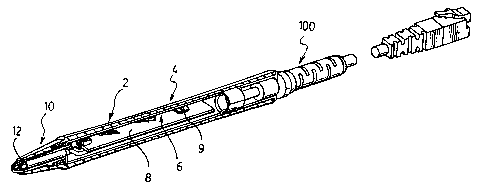
| (54) English Title: | SIGNALING PEN |
| (54) French Title: | STYLET A SIGNALISATION |
| Status: | Granted and Issued |
| (51) International Patent Classification (IPC): |
|
|---|---|
| (72) Inventors : |
|
| (73) Owners : |
|
| (71) Applicants : |
|
| (74) Agent: | BLAKE, CASSELS & GRAYDON LLP |
| (74) Associate agent: | |
| (45) Issued: | 2011-07-05 |
| (22) Filed Date: | 2005-04-19 |
| (41) Open to Public Inspection: | 2006-10-19 |
| Examination requested: | 2005-10-05 |
| Availability of licence: | N/A |
| Dedicated to the Public: | N/A |
| (25) Language of filing: | English |
| Patent Cooperation Treaty (PCT): | No |
|---|
| (30) Application Priority Data: | None |
|---|
A signaling pen of improved construction includes an actuator that functions generally independent of a bias and stop arrangement. Preferably an antenna is fixed to a PCB board secured within a body. This provides an efficient signal communication path. Preferably the PCB board is secured within an inner casing that also houses the ON/OFF actuator. An extension of the displaceable pen tip extends into said casing and controls the ON/OFF actuator.
Stylet à signalisation dont la construction a été améliorée. Il comprend un actionneur qui fonctionne généralement indépendamment d'un circuit de polarisation et d'arrêt. De préférence, une antenne est fixée à une carte de circuits imprimés immobilisée dans un corps. Cela offre un trajet de communication des signaux efficient. De préférence, la carte de circuits imprimés est immobilisée dans un boîtier intérieur qui abrite aussi l'actionneur ON/OFF. Un prolongement de la pointe du stylet mobile s'étend dans ledit boîtier et commande l'actionneur ON/OFF.
Note: Claims are shown in the official language in which they were submitted.
Note: Descriptions are shown in the official language in which they were submitted.
2024-08-01:As part of the Next Generation Patents (NGP) transition, the Canadian Patents Database (CPD) now contains a more detailed Event History, which replicates the Event Log of our new back-office solution.
Please note that "Inactive:" events refers to events no longer in use in our new back-office solution.
For a clearer understanding of the status of the application/patent presented on this page, the site Disclaimer , as well as the definitions for Patent , Event History , Maintenance Fee and Payment History should be consulted.
| Description | Date |
|---|---|
| Revocation of Agent Requirements Determined Compliant | 2020-08-27 |
| Appointment of Agent Requirements Determined Compliant | 2020-08-27 |
| Change of Address or Method of Correspondence Request Received | 2020-08-07 |
| Revocation of Agent Request | 2020-08-07 |
| Appointment of Agent Request | 2020-08-07 |
| Appointment of Agent Requirements Determined Compliant | 2020-07-27 |
| Inactive: Office letter | 2020-07-27 |
| Revocation of Agent Requirements Determined Compliant | 2020-07-27 |
| Inactive: Adhoc Request Documented | 2020-07-07 |
| Appointment of Agent Request | 2020-05-20 |
| Revocation of Agent Request | 2020-05-20 |
| Change of Address or Method of Correspondence Request Received | 2020-05-20 |
| Appointment of Agent Request | 2020-04-07 |
| Revocation of Agent Request | 2020-04-07 |
| Inactive: COVID 19 - Deadline extended | 2020-03-29 |
| Change of Address or Method of Correspondence Request Received | 2020-03-24 |
| Maintenance Request Received | 2020-03-24 |
| Common Representative Appointed | 2019-10-30 |
| Common Representative Appointed | 2019-10-30 |
| Inactive: First IPC assigned | 2013-01-17 |
| Inactive: IPC removed | 2013-01-17 |
| Inactive: IPC assigned | 2013-01-17 |
| Inactive: IPC expired | 2013-01-01 |
| Inactive: IPC removed | 2012-12-31 |
| Inactive: IPC deactivated | 2011-07-29 |
| Grant by Issuance | 2011-07-05 |
| Inactive: Cover page published | 2011-07-04 |
| Pre-grant | 2011-04-18 |
| Inactive: Final fee received | 2011-04-18 |
| Letter Sent | 2011-03-07 |
| Notice of Allowance is Issued | 2011-03-07 |
| Notice of Allowance is Issued | 2011-03-07 |
| Inactive: Approved for allowance (AFA) | 2011-02-28 |
| Amendment Received - Voluntary Amendment | 2009-12-08 |
| Inactive: S.30(2) Rules - Examiner requisition | 2009-06-08 |
| Application Published (Open to Public Inspection) | 2006-10-19 |
| Inactive: Cover page published | 2006-10-18 |
| Inactive: IPC assigned | 2006-02-08 |
| Inactive: First IPC assigned | 2006-02-08 |
| Inactive: IPC assigned | 2006-02-08 |
| Letter Sent | 2006-02-06 |
| All Requirements for Examination Determined Compliant | 2005-10-05 |
| Request for Examination Requirements Determined Compliant | 2005-10-05 |
| Request for Examination Received | 2005-10-05 |
| Inactive: Payment - Insufficient fee | 2005-09-21 |
| Letter Sent | 2005-09-08 |
| Request for Examination Received | 2005-07-20 |
| Amendment Received - Voluntary Amendment | 2005-07-20 |
| Inactive: Single transfer | 2005-07-20 |
| Inactive: First IPC assigned | 2005-06-10 |
| Inactive: Filing certificate - No RFE (English) | 2005-05-09 |
| Filing Requirements Determined Compliant | 2005-05-09 |
| Inactive: Courtesy letter - Evidence | 2005-05-09 |
| Application Received - Regular National | 2005-05-09 |
There is no abandonment history.
The last payment was received on 2011-04-18
Note : If the full payment has not been received on or before the date indicated, a further fee may be required which may be one of the following
Please refer to the CIPO Patent Fees web page to see all current fee amounts.
Note: Records showing the ownership history in alphabetical order.
| Current Owners on Record |
|---|
| INGENICO CANADA LTD. |
| Past Owners on Record |
|---|
| JONATHAN DAVID LIBERTY |
| KI SHEUNG YUEN |
| XIAOYU ZHOU |

