Sélection de la langue

Search

Sommaire du brevet 2503204 

Énoncé de désistement de responsabilité concernant l'information provenant de tiers

Une partie des informations de ce site Web a été fournie par des sources externes. Le gouvernement du Canada n'assume aucune responsabilité concernant la précision, l'actualité ou la fiabilité des informations fournies par les sources externes. Les utilisateurs qui désirent employer cette information devraient consulter directement la source des informations. Le contenu fourni par les sources externes n'est pas assujetti aux exigences sur les langues officielles, la protection des renseignements personnels et l'accessibilité.

Disponibilité de l'Abrégé et des Revendications

L'apparition de différences dans le texte et l'image des Revendications et de l'Abrégé dépend du moment auquel le document est publié. Les textes des Revendications et de l'Abrégé sont affichés :

  • lorsque la demande peut être examinée par le public;
  • lorsque le brevet est émis (délivrance).
(12) Brevet: (11) CA 2503204
(54) Titre français: STYLET A SIGNALISATION
(54) Titre anglais: SIGNALING PEN
Statut: Octroyé
Données bibliographiques
(51) Classification internationale des brevets (CIB):
  • G06F 3/0354 (2013.01)
(72) Inventeurs :
  • YUEN, KI SHEUNG (Canada)
  • ZHOU, XIAOYU (Canada)
  • LIBERTY, JONATHAN DAVID (Canada)
(73) Titulaires :
  • INGENICO CANADA LTD. (Canada)
(71) Demandeurs :
  • INGENICO CANADA LTD. (Canada)
(74) Agent: BLAKE, CASSELS & GRAYDON LLP
(74) Co-agent:
(45) Délivré: 2011-07-05
(22) Date de dépôt: 2005-04-19
(41) Mise à la disponibilité du public: 2006-10-19
Requête d'examen: 2005-10-05
Licence disponible: S.O.
(25) Langue des documents déposés: Anglais

Traité de coopération en matière de brevets (PCT): Non

(30) Données de priorité de la demande: S.O.

Abrégés

Abrégé français

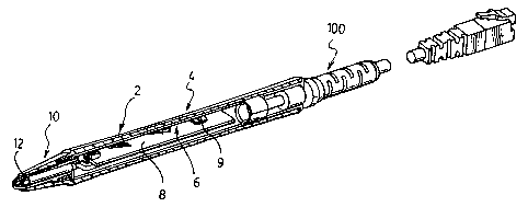
Stylet à signalisation dont la construction a été améliorée. Il comprend un actionneur qui fonctionne généralement indépendamment d'un circuit de polarisation et d'arrêt. De préférence, une antenne est fixée à une carte de circuits imprimés immobilisée dans un corps. Cela offre un trajet de communication des signaux efficient. De préférence, la carte de circuits imprimés est immobilisée dans un boîtier intérieur qui abrite aussi l'actionneur ON/OFF. Un prolongement de la pointe du stylet mobile s'étend dans ledit boîtier et commande l'actionneur ON/OFF.


Abrégé anglais

A signaling pen of improved construction includes an actuator that functions generally independent of a bias and stop arrangement. Preferably an antenna is fixed to a PCB board secured within a body. This provides an efficient signal communication path. Preferably the PCB board is secured within an inner casing that also houses the ON/OFF actuator. An extension of the displaceable pen tip extends into said casing and controls the ON/OFF actuator.

Revendications

Note : Les revendications sont présentées dans la langue officielle dans laquelle elles ont été soumises.


THE EMBODIMENTS OF THE INVENTION IN WHICH AN EXCLUSIVE
PROPERTY OR PRIVILEGE IS CLAIMED ARE DEFINED AS FOLLOWS:

1. An electronic signaling pen comprising an
antenna,
a pen tip movable relative to a casing between an
OFF position and an ON position with a spring bias urging
said pen tip to said OFF position, said casing including
a PCB board secured therein,
said pen tip including an actuator that cooperates
with an actuation point of a circuit of said PCB board
and changes the state of said circuit dependent upon the
ON/OFF position of said pen tip, said actuator in said ON
position causing said circuit to conduct and in said OFF
position, causing said circuit to be open; and wherein
said pen tip includes a separate stop arrangement that
determines the ON position of said pen tip.

2. An electronic signaling pen as claimed in claim 1
wherein said PCB board includes an antenna fixed to said
PCB board.

3. An electronic signaling pen as claimed in claim 2
wherein said pen tip moves relative to said antenna as
said pen tip moves between said OFF position to the ON
position.

4. An electronic signaling pen as claimed in claim 3
wherein the movement of said pen tip between the ON and
OFF positions is less than 1 mm.

5. An electronic signaling pen as claimed in claim 1
wherein said actuator is a compressible member secured on
an end portion of said pen tip.

6. An electronic signaling pen as claimed in claim 5
wherein said compressible member includes an electrical


-9-


conducting portion at a free end thereof that completes
an electrical connection with said actuation point PCB
board when said pen tip is in said ON position.

7. An electronic signaling pen as claimed in claim 1
including an outer protective sleeve about said casing
with said pen tip movable relative to said outer
protective sleeve.

8. An electronic signaling pen as claimed in claim 7
wherein said casing is a split plastic molded casing.

9. An electronic signaling pen as claimed in claim 8
wherein said split plastic molded casing is plated with
an electrically conductive material and includes a ground
arrangement for grounding said PCB board.

10. An electronic signaling pen as claimed in claim 9
wherein said casing adjacent said pen tip includes a port
extending through said casing and said pen tip includes
an extension member connected to said pen tip and
extending into said casing, said extension member
including a compressible switch actuator engaging said
actuation point of said PCB board when said pen tip is in
the ON position.

11. An electronic signaling pen as claimed in claim 10
wherein said compressible switch actuator includes an
integral electrically conducting member at the end
thereof that engages stationary electrical conducting
points of said actuation point and completes an
electrical conduction path of said circuit.

12. An electronic signaling pen as claimed in claim 11
wherein said pen tip when assembled on said casing is
captured thereon.


-10-


13. An electronic signaling pen as claimed in claim 12
wherein said compressible switch actuator is resiliently
compressed as said pen tip moves between said OFF and
said ON positions.

14. An electronic signaling pen as claimed in claim 13
wherein said molded casing includes an antenna sleeve
projecting from one end of said casing into said pen tip.

15. An electronic signaling pen as claimed in claim 14
wherein said antenna is a wire soldered to said PCB
board.

16. An electronic signaling pen as claimed in claim 1
wherein said antenna is a wire soldered to said PCB
board.

17. An electronic pen comprising a pen body, an
electronic circuit secured in said pen body and said
electronic circuit includes a stationary part of an
ON/OFF actuator, a movable pen tip secured at one end of
said body that is spring biased to an extended position
relative to said pen body and is movable to an actuating
position partially telescoped within said pen body, said
pen tip including a moving part of said ON/OFF actuator,
said moving part including an electrical conducting
member that forms an electrical connection with said
stationary part turning said actuator ON when said pen
tip is in said actuating position, said moving part
breaking any electrical connection with said stationary
part as said pen tip moves from said actuating position
to said extended position and thereby turning said
actuator OFF when said pen tip is in said extended
position, and wherein said electronic circuit includes an
antenna having a fixed connection with said electronic
circuit.


-11-


18. An electronic pen as claimed in claim 17 wherein
said moving part of said actuator is a compressible
member fixed on said pen tip interior to said pen body.

19. An electronic pen as claimed in claim 18 wherein
said pen tip cooperates with a structural element of said
pen body to provide a stop surface defining said
actuating position.

20. An electronic pen as claimed in claim 17 wherein
said pen includes a stop surface separate from said
ON/OFF actuator, said stop face determining the extent
that said pen tip can telescope within said pen body.

21. An electronic pen comprising a pen body, an
electronic circuit secured in said body and said
electronic circuit including a stationary part of an
ON/OFF actuator, a movable pen tip secured at one end of
said body that is spring biased to an extended position
relative to said pen body and is movable to an actuating
position partially telescoped within said pen body, said
pen tip including an moving part of said ON/OFF actuator,
said moving part including an electrical conducting
member that forms a first electrical state with said
stationary part turning said actuator ON when said pen
tip is in said actuating position, said moving part
changing said first state to a second electrical state
turning said actuator OFF as said pen tip moves from said
actuating position to said extended position, and wherein
said electronic circuit includes an antenna having a
fixed connection with said electronic circuit.

22. An electronic pen as claimed in claim 21 wherein
said moving part of said actuator is a compressible
member fixed on said pen tip on a portion of said pen tip
extending into an interior chamber portion of said pen
body that houses said electronic circuit.


-12-


23. An electronic pen as claimed in claim 22 wherein
said pen tip cooperates with a structural element of said
pen body to provide a stop surface defining said
actuating position that limits the inward telescopic
movement of said pen tip.

24. An electronic pen as claimed in claim 21 wherein
said pen includes a stop surface separate from said
ON/OFF actuator.

25. An electronic pen as claimed in claim 22 wherein
said spring bias in said ON position generates a force at
least a order of magnitude greater than a force generated
due to compression of said compressible member when said
actuator is in said ON position.


-13-

Description

Note : Les descriptions sont présentées dans la langue officielle dans laquelle elles ont été soumises.


WH 12 647CA
CA 02503204 2005-07-20
TITLE: SIGNALING PEN
FIELD OF THE INVENTION
The present invention relates to a digital pen for
use in association with a digitizing surface.
BACKGROUND OF THE INVENTION
An electronic signaling device in the form of a
pen or stylus has been used for many years in association
with a digitizing surface. Basically, the stylus
cooperates with the digitizing surface to determine the
particular pattern of movement of the pen as it moves
across the surface and provides a digital record thereof.
These types of devices are used for a host of
applications but have particular application in
association with check writing and/or digital signatures.
The technology for using a digital pen is quite
well known and requires a user to place the pen on the
appropriate surface and displaces a tip portion to
activate the device as part of the normal writing
process. The pen transmits or receives a signal
depending on the particular application and in any event,
the particular position of the pen on the surface is
determined. As the pen is moved across the surface, the
particular pattern is recorded and typically visually
reproduced on the device.
Although digital pens have been known for many
years, the construction of the pens is complicated and
the assembly of the components of the pen requires
considerable precision and time.
The present invention provides a simplified
electronic pen which is cost effective to manufacture.
- 1 -

CA 02503204 2005-07-20
WH 12 647CA
SUMMARY OF THE INVENTION
An electronic signaling pen according to the
present invention comprises an antenna and a pen tip
movable relative to a casing which secures a printed
circuit board (PCB). The pen tip is movable between an
OFF position and an ON position with a spring bias urging
the pen tip to the OFF position. The pen tip includes an
actuator independent of the antenna that cooperates with
a contact point of a circuit of the PCB board and changes
the state of the circuit dependent upon the position of
the pen tip in the ON or OFF position. The pen tip
includes a stop arrangement that limits the extent that
the tip moves towards the casing.
According to an aspect of the invention, the PCB
board includes an antenna fixed to the PCB board.
According to a further aspect of the invention the
pen tip moves relative to the antenna as the pen tip
moves between the OFF position and the ON position.
In yet a further aspect of the invention, the
movement of the pen tip between the ON and OFF positions
is less than lmm.
In yet a further aspect of the invention, the
actuator includes compressible material secured on an end
portion of the pen tip.
In yet a further aspect of the invention, the
compressible material includes an electrical conducting
portion at a free end thereof that engages and completes
an electrical condition with the PCB board when the pen
tip is in the ON position.
In a different aspect of the invention, the pen
includes an outer protective sleeve about the casing of
- 2 -

CA 02503204 2005-07-20
WH 12 647CA
the pen and the pin tip is movable relative to the outer
protective sleeve.
In yet a different aspect of the invention, the
signaling pen has a split plastic molded casing about the
circuit board and secures the circuit board. This
plastic mold casing is plated with an electrically
conducted material and includes a ground arrangement for
grounding of the PCB board.
In yet a different aspect of the invention, the
casing adjacent the pen tip includes a port extending
through the casing and the pen tip includes an extension
member connected to the pen tip and extending into the
casing. The extension member includes a compressible
switch actuator engaging the PCB board when the pen tip
is in the ON position.
An electronic pen according to the present
invention comprises a pen body, an electronic circuit
secured in the body with the electronic circuit including
a stationary part of an ON/OFF actuator. A movable pen
tip is secured at one end of the body and is spring
biased to an extended position relative to the pen body.
The pen tip is movable to an actuating position partially
telescoped within the pen body. The pen body includes a
moving part of the ON/OFF actuator. This moving part
includes an electrical conducting member that forms an
electrical connection with the stationary part turning
the actuator ON when the pen tip is in the actuating
position. The moving part breaks any electrical
connection with the stationary part as the pen tip moves
from the actuating position to the extended position.
The electronic circuit includes antenna preferably having
a fixed connection with the electronic circuit.
- 3 -

CA 02503204 2005-07-20
WH 12 647CA
According to an aspect of the invention, the
moving part of the actuator is a compressible member
fixed on the pen tip interior to the pen body.
In a different aspect of the invention, the pen
tip cooperates with a structural element of the pen body
to provide a stop surface defining the actuating
position.
In a different aspect of the invention, the pen
includes a stop surface separate from said ON/OFF
actuator that defines said actuating position.
BRIEF DESCRIPTION OF THE DRAWINGS
Preferred embodiments of the invention are shown
in the drawings, wherein:
Figure 1 is a partial perspective cutaway view of
the electronic pen;
Figure 2 is a sectional view through the
electronic pen;
Figure 3 is a partial sectional view showing the
cooperation of the movable pen tip and pen body;
Figure 4 is a sectional view similar to Figure 2
but with the pen tip in an actuating position;
Figure 5 is a partial sectional view showing the
pen tip in the actuating position;
Figure 6 is an exploded view showing the various
components of the electronic pen;
Figure 7 is a partial perspective view of the pen
tip and pen body; and
Figure 8 is a partial perspective view of the pen
casings.
DETAILED DESCRIPTION OF THE PREFERRED EMBODIMENTS
The electrical pen 2 includes an outer pen body 4
housing an inner casing 6. The inner casing is
- 4 -

CA 02503204 2005-07-20
WH 12 647CA
positioned within the outer pen body by guides and houses
the PCB circuit board 8. The displaceable tip 10
telescopes within the outer pen body 4 and moves between
an extended position as shown in Figures 1 and 3 to an
actuating position or ON position as shown in Figures 4
and 5.
The displaceable tip 10 protects the fixed antenna
12. Preferably the antenna is a wire soldered on the PCB
circuit board 8. This provides an effective electrical
connection of the antenna 12 to the PCB board. Other
electrical connections of the antenna to the PCB board
are possible, however, it is preferred that the antenna
be fixed on the board to provide an effective signal
path. There is no movement of the antenna relative to
the PCB board during movement of the displaceable tip 10
from the extended position to the actuating position. In
a preferred embodiment the wire antenna is a conventional
wire. For example, 24 awg wire performs well.
The displaceable tip 10 is preferably an injection
molded plastic member and carries a movable part 20 of
the ON/OFF actuator 16. The PCB board 8 includes a
stationary part defined by two spaced conductors 18 which
cooperate with the electrical conducting surface 22 of
the movable part 20. As the pen tip moves from the
extended position of Figure 1 to the actuating position
of Figures 4 and 5, the movable part 20 which is a
compressible member moves with the pen tip and applies a
low pressure force on the two spaced conductors 18 due to
compression of the movable member. The resilient
compression of member 20 provides an efficient connection
of the electrical conducting surface 22 with the
electrical conductors 18 of the ON/OFF actuator 16.
With the present design, the movable part 20
undergoes compression and thus a pressure force is
exerted to provide an effective connection of the two
- 5 -

CA 02503204 2005-07-20
WH 12 647CA
electrical connectors 18 of the stationary part of the
actuator 16. Compressible member 20 does not
significantly act to stop the movement of the
displaceable tip 10. This movement is stopped due to an
interference contact between the displaceable tip 10 and
in this case, the end of the inner casing 6. The bias
spring 30 produces a force much greater (at least an
order of magnitude greater) than the compression force
generated by member 30. Thus the resilient compression
force of member 30 does not significantly influence the
bias force of the spring.
As shown in Figure 5, extension 52 of the pen tip
bottoms against the end 54 of the casing 8. The bias
spring 30 provides some resistance, however, it is the
engagement of extension 52 and 54 of the casing that
provides the positive stop and determines the actuating
position of the pen tip. When pressure on the pen tip is
removed, i.e. the pen tip is not in writing contact with
a surface, the bias spring 30 forces the displaceable pen
tip 10 to the extended position as shown in Figures 1, 2
and 3.
As shown in the partial sectional view of Figure
3, electrical conducting surface 22 of the movable part
20 is now spaced from the electrical conductors 18 of the
stationary part of the ON/OFF actuator 16.
The inner casing 6 includes a first casing 66 and
a second casing 68 and these casings include a port 60
through which the projecting arm 62 of the pen tip 10
extends. With this arrangement, the movable part 20 is
located within the casing 6 and is quickly actuated by
means of the movement of the pen tip to the actuating
position. It can also be appreciated that the antenna 12
is stationary and includes an excellent electrical
connection with the PCB board 8.
- 6 -

CA 02503204 2005-07-20
wH 12 647cA
As shown in Figure 6, the first casing 66 includes
a guide tube 70 which is sized to receive the antenna 12.
The antenna is secured on the PCB board 8 and is then
located together with the PCB board between the two
casings. The first casing 66 and the second casing 68
cooperate to positively secure the PCB board 8 in a fixed
position within the casing. Each of the casings 66 and
68 are a plastic molded component that is electrically
plated with a conductive metal. The PCB extends across
the two casings such that the split lines are above and
below the PCB board. The metal plated casings act as a
shield electrically protecting the PCB board from
extraneous signals. Only the portion of the antenna
beyond the casing is outside the shield whereby improved
performance is achieved.
The casings cooperate, as shown in Figures 2 and
4, where the grounding flanges 78 and 80 of the casings
engage appropriate electrical contact portions 9 on the
PCB board 8. This provides a common voltage reference to
the PCB board and the assembled casing. A ground sleeve
74 is then applied over the metal plating of the casings
(see Figure 8).
The PCB board 8 and the casings are assembled in a
simple manner and the displaceable tip 12 is also
assembled on the casings. This is required as the
movable compressible part 20 is located within the
casing. Therefore, the displaceable tip 10, the spring
30 and the movable part 20 are assembled on the
cooperating first and second casings 66 and 68. Once
this arrangement has been assembled, it can then be
inserted into the open end 90 of the outer body pen
portion 4. The inner casing 6 is moved to the bottom end
of the outer pen body 4 until it engages a stop or
locating flange such as flange 32. The spring relief
provided by the rubber portion of the electrical
_ 7 _

CA 02503204 2005-07-20
WH 12 647CA
conductor 100 closes the end of the pen body and locks
the casing 6 in position.
The general assembly of the pen is as follows:
The electrical power conductor 100 and the antenna 12 are
soldered to the PCB board. The PCB board is then
positioned in the casing 66 and the antenna is placed in
the tube 70 (see Figure 7). A bare portion of the
antenna extends beyond the casing. The pen tip and
actuator are assembled on the casing 66. The other
casing 68 is then assembled to enclose the PCB board.
The assembled unit is inserted into the pen body and
locks therewith.
The metal plate casing and PCB board are grounded
when the pen is actuated and a sinusoidal signal is
provided to the casing when the pen is not actuated.
This particular arrangement has proven to be
effective partially due to the effective electrical
connection of the antenna to the PCB board as well as the
action of ON/OFF actuator 16 that operates essentially
independently of a stop mechanism. The number of moving
parts has been reduced and the ability to provide high
quality control is realized. The ON/OFF actuator and the
pen tip operate quickly without any large movement of the
displaceable pen tip. This improves the feel of the pen
to a user.
Although various preferred embodiments of the
present invention have been described herein in detail,
it will be appreciated by those skilled in the art that
variations may be made thereto without departing from the
spirit of the invention or the scope of the appended
claims.
_ g

Dessin représentatif
Une figure unique qui représente un dessin illustrant l'invention.
États administratifs

Pour une meilleure compréhension de l'état de la demande ou brevet qui figure sur cette page, la rubrique Mise en garde , et les descriptions de Brevet , États administratifs , Taxes périodiques et Historique des paiements devraient être consultées.

États administratifs

Titre Date
Date de délivrance prévu 2011-07-05
(22) Dépôt 2005-04-19
Requête d'examen 2005-10-05
(41) Mise à la disponibilité du public 2006-10-19
(45) Délivré 2011-07-05

Historique d'abandonnement

Il n'y a pas d'historique d'abandonnement

Historique des paiements

Type de taxes Anniversaire Échéance Montant payé Date payée
Le dépôt d'une demande de brevet 400,00 $ 2005-04-19
Enregistrement de documents 100,00 $ 2005-07-20
Requête d'examen 800,00 $ 2005-10-05
Taxe de maintien en état - Demande - nouvelle loi 2 2007-04-19 100,00 $ 2007-04-16
Taxe de maintien en état - Demande - nouvelle loi 3 2008-04-21 100,00 $ 2008-04-18
Taxe de maintien en état - Demande - nouvelle loi 4 2009-04-20 100,00 $ 2009-04-14
Taxe de maintien en état - Demande - nouvelle loi 5 2010-04-19 200,00 $ 2010-04-15
Taxe finale 300,00 $ 2011-04-18
Taxe de maintien en état - Demande - nouvelle loi 6 2011-04-19 200,00 $ 2011-04-18
Taxe de maintien en état - brevet - nouvelle loi 7 2012-04-19 200,00 $ 2012-03-27
Taxe de maintien en état - brevet - nouvelle loi 8 2013-04-19 200,00 $ 2013-01-25
Taxe de maintien en état - brevet - nouvelle loi 9 2014-04-22 200,00 $ 2014-03-21
Taxe de maintien en état - brevet - nouvelle loi 10 2015-04-20 250,00 $ 2015-02-11
Taxe de maintien en état - brevet - nouvelle loi 11 2016-04-19 250,00 $ 2016-03-04
Taxe de maintien en état - brevet - nouvelle loi 12 2017-04-19 250,00 $ 2017-04-11
Taxe de maintien en état - brevet - nouvelle loi 13 2018-04-19 250,00 $ 2018-04-13
Taxe de maintien en état - brevet - nouvelle loi 14 2019-04-23 250,00 $ 2019-04-17
Taxe de maintien en état - brevet - nouvelle loi 15 2020-04-20 450,00 $ 2020-03-24
Taxe de maintien en état - brevet - nouvelle loi 16 2021-04-19 459,00 $ 2021-03-25
Taxe de maintien en état - brevet - nouvelle loi 17 2022-04-19 458,08 $ 2022-01-17
Taxe de maintien en état - brevet - nouvelle loi 18 2023-04-19 473,65 $ 2023-04-05
Taxe de maintien en état - brevet - nouvelle loi 19 2024-04-19 624,00 $ 2024-03-25
Titulaires au dossier

Les titulaires actuels et antérieures au dossier sont affichés en ordre alphabétique.

Titulaires actuels au dossier
INGENICO CANADA LTD.
Titulaires antérieures au dossier
LIBERTY, JONATHAN DAVID
YUEN, KI SHEUNG
ZHOU, XIAOYU
Les propriétaires antérieurs qui ne figurent pas dans la liste des « Propriétaires au dossier » apparaîtront dans d'autres documents au dossier.
Documents

Pour visionner les fichiers sélectionnés, entrer le code reCAPTCHA :


Pour visualiser une image, cliquer sur un lien dans la colonne description du document. Pour télécharger l'image (les images), cliquer l'une ou plusieurs cases à cocher dans la première colonne et ensuite cliquer sur le bouton "Télécharger sélection en format PDF (archive Zip)" ou le bouton "Télécharger sélection (en un fichier PDF fusionné)".

Liste des documents de brevet publiés et non publiés sur la BDBC .

Si vous avez des difficultés à accéder au contenu, veuillez communiquer avec le Centre de services à la clientèle au 1-866-997-1936, ou envoyer un courriel au Centre de service à la clientèle de l'OPIC.


Description du
Document 
Date
(yyyy-mm-dd) 
Nombre de pages   Taille de l'image (Ko) 
Paiement de taxe périodique 2020-03-24 3 46
Changement à la méthode de correspondance 2020-03-24 3 46
Page couverture 2006-10-05 1 36
Abrégé 2005-04-19 1 14
Description 2005-04-19 8 337
Revendications 2005-04-19 5 185
Paiement de taxe périodique 2023-04-05 1 33
Dessins 2005-07-20 4 87
Description 2005-07-20 8 325
Dessins représentatifs 2006-09-26 1 11
Page couverture 2011-06-07 1 36
Correspondance 2005-05-09 1 25
Cession 2005-04-19 3 86
Poursuite-Amendment 2005-07-20 14 458
Cession 2005-07-20 5 140
Poursuite-Amendment 2009-12-08 3 134
Poursuite-Amendment 2005-10-05 1 28
Correspondance 2011-04-18 2 41
Poursuite-Amendment 2009-06-08 3 117