Note: Descriptions are shown in the official language in which they were submitted.
CA 02503306 2005-03-30
SYSTEM AND METHOD FOR INTRA-CABINET WIRELESS
COMMUNICATION
Field of the Invention
This invention relates in general to technologies for broadband wireless
component
cabinets. This invention relates more particularly to systems and methods for
enabling wireless communication between broadband network components within a
cabinet.
Background of the Invention
Communication equipment in telecom, datacom, professional audio and video, and
harsh environments is typically designed to be installed within one or more
cabinets,
of the type illustrated in Figure I . Each cabinet usually conforms to the EIA
(Electronics Industry Association) standard width of 19 or 23 inches and
houses a
multitude of card cages or rack units. Rack units in turn house a number of
circuit
pack modules (also referred to as electronic circuit packs). A representative
rack unit
is also illustrated in Fig. 7a.
Each rack unit andlor circuit pack module within a rack unit typically
requires the
establishment of a multitude of communication links to effect intra-cabinet
communication among collocated equipment. Traditionally, this intra-cabinet
communication has been physically established using either electrical or
optical
interconnect cables (as illustrated in Fig. 1), and usually creating from such
cables
well known network topologies including star, ring, bus, and mesh. Cable
systems,
however, suffer from a number of shortcomings. Use of electrical or optical
interconnect cables in many implementations results in cable clutter, which
obstructs
air flow for cooling, and interferes with moves/adds/changes. The complex
cable
3o arrangements involved typically require skilled technicians to install and
maintain
them over the course of their life. Electrical cables do not offer
catastrophic fault
isolation from surges, immunity to ground loop EMI (Electromagnetic
Interference),
CA 02503306 2005-03-30
-2-
nor immunity to common mode range issues associated with ground referenced
systems. The optical connectors and transceivers used in such cable systems
for
providing intra-cabinet communication are generally relatively costly. The
optical
and electrical cables and cable harness assemblies that are used are typically
made
specifically for the particular cabinet and for its installed racks, card
cages, and circuit
pack modules. As a result these components generally: (A) increase
commissioning
time and complexity, and (B) Require specialized knowledge for installation,
maintenance, and moves/adds/changes. On occasion, connector pins and threads
can
be become damaged if improperly installed resulting in costly field repair
work.
Optical and electrical cables used generally employ mechanical connectors that
are
sensitive to relatively common environmental factors such as dust, humidity,
sea salt,
temperature, thermal cycling and vibration.
What is needed therefore is a system and method for providing wireless
communication between the aforesaid components in a cabinet.
United States Patent No. 6,771,935 ('935) issued to Leggett discloses a
wireless bus
that replaces the hard-wired mid plane bus utilized in a standard
telecommunication
switch. Rather than using the usual wired connections between the mid plane
bus and
2o the various circuit boards or cards, a plurality of radio frequency
antennae or probes
are used for each such circuit board or card. The antennae or probes project
into a
common waveguide. By virtue of this arrangement, each circuit board or card is
operable to communicate with the other circuit boards or cards on
predetermined
radio channels. '935 also discloses containment of the cards and their
antennae within
a conductive enclosure to permit wireless communication between components
separated by intervening objects.
One disadvantage of the technology disclosed in '935 is that reflection of
incident
electromagnetic radiation off of the walls of the disclosed waveguide will
generally
3o result in multi path distortion. '935 does not disclose adequate means for
mitigating
such multi path distortion. The invention described in '935 could lead to a
high
number of sustained reflections of the electromagnetic radiation and therefore
the
CA 02503306 2005-03-30
-3-
communication channel capacity will be limited and/or the complexity of the
required
receiver will be significantly greater.
Also, it should be noted that '935 focuses on back plane/mid plane
substitutive
technology. Mid plane and back plane structures are typically constructed from
Printed Circuit Board ("PCB") materials and are generally limited in size to
less than
60cm x 50 cm. These mid plane and back plane structures are usually integrated
into a
rack mount card cage that is subsequently installed within a cabinet. As
stated earlier,
a cabinet typically contains a number of these rack units that need to
intercommunicate. The '935 technology therefore addresses intra-card cage
communication only, whereas there is a need for a technology that provides
wireless
communication between multiple points throughout the interior of the cabinet,
including between the various components whether the are located on the same
or
different card cages.
It is also noted neither '935 nor any other prior art address the issue of
bandwidth
management within the cabinet.
What is needed therefore is a system and method for providing intra-cabinet
2o communication between the various broadband network components. A system
and
method is required that enables wireless communication between the various
broadband network components located throughout the interior of the cabinet,
while
minimizing the effects of multi-path signal distortion. A system and method is
also
required that enables the deployment of wireless intra-cabinet communication
that is
easy to implement, and requires relatively inexpensive components. Also, there
is a
need for a system and method that permits efficient allocation of channel
resources
across domains, including SDMA, FDMA, TDMA, CDMA and PDMA domains
(defined below), within the confines of the cabinet.
CA 02503306 2005-03-30
-4-
Summary of the Invention
The present invention provides a solution for enabling intra-cabinet
communication
between the various components stored in a cabinet.
In one aspect thereof, the present invention provides a wireless multi-linking
system
for enabling electronic components disposed inside a cabinet to inter-
communicate
wirelessly, the system comprising: (a) a plurality of wireless multi-link
devices
linked, directly or indirectly, to a plurality of the electronic components,
the wireless
1o multi-link devices including one or more radiating elements; and (b) an
RF/microwave chamber within or adjacent to the cabinet wherein at least one
dimension of the RF/microwave chamber is greater than'/2 the wavelength of the
lowest signal frequency of each of the wireless multi-link devices at their
range of
operation, wherein the RFlmicrowave chamber is disposed so as to confine the
15 radiating elements and is operable to substantially confine signals emitted
by the
radiating elements within the RF/microwave chamber; wherein the wireless multi-
link
devices are operable to connect to a wireless medium provided within the
RF/microwave chamber and to inter-communicate via the wireless medium by
operation of the radiating elements, thereby enabling inter-communication
between
2o the plurality of electronic components.
The RF/microwave chamber of the present invention can either be provided in
existing cabinets, or new cabinets can be manufactured such that they include
or
accommodate the RF/microwave chamber of the present invention.
A number of different embodiments of the RF/microwave chamber are also
provided
to adapt to different conditions inside the cabinet, and also to provide
different
arrangements of the RF/microwave chamber to facilitate increased intra-cabinet
communication capacity and to reduce multi-path signal distortion.
In another aspect of the invention, a method is provided for linking
electronic
components disposed inside a cabinet for wireless communication therebetween.
This
CA 02503306 2005-03-30
method can be used in providing cabinets that include the RF/microwave chamber
of
the present invention, or to modify existing cabinets to include the
RF/microwave
chamber.
In another aspect of the present invention, a wireless transceiver is provided
that is
operable to manage wireless inter-connection between a plurality of wireless
electronic components, including in the RF/microwave chamber air medium.
In a still other aspect of the present invention a new circuit card is
provided that
1 o includes the wireless transceiver. A further aspect of the present
invention is a circuit
card that includes the wireless transceiver and also a radiating unit for
providing intra-
cabinet communication within the RF/microwave chamber.
The RF/microwave chamber and the wireless transceiver of the present invention
can
15 be utilized in environments other than a cabinet where wireless
communication
between wired components is desirable.
Brief Description of the Drawings
20 A detailed description of the preferred embodiments) is (are) provided
herein
below by way of example only and with reference to the following drawings, in
which:
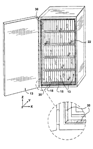
Figure 1 is a front perspective view illustrating the principal physical
features
25 of a cabinet for broadband network components;
Figure 2 is a back perspective view further illustrating the principal
physical
features of a cabinet for broadband network components;
30 Figure 3 is a perspective view of a representative circuit pack module;
CA 02503306 2005-03-30
-6-
Figure 4 is a further perspective view of the cabinet, illustrating within the
cabinet the RF/microwave chamber of the present invention;
Figure Sa illustrates a particular embodiment of the RFlmicrowave chamber,
which is a six-sided chamber that includes an outer conductive shield and an
inner
lining of frequency absorption material;
Figure Sb is a cross-sectional view of the embodiment illustrated in Figure
Sa;
Figure 6a illustrates the intra-cabinet communication unit of the present
invention, in a perspective view thereof;
Figure 6b illustrates a transceiver module in a surface mount SOP with
optional integrated radiating unit;
Figure 6c illustrates a standalone transceiver module in a surface mount SOP
mounted on a circuit pack with the radiating unit formed therein;
Figure 7a illustrates a representative card cage;
Figure 7b in a perspective view illustrates a PCB card that plugs into a
backplane rack mount card cage, in which the intra-cabinet wireless
transceiver of the
present invention is mounted on the PCB card;
Figure 7c illustrates circuit packs mounted horizontally within a card cage
for
placement in the cabinet;
Figure 7d illustrates circuit packs mounted horizontally and vertically within
a
card cage for placement in the cabinet;
Figure 7e illustrates a card cage with integral non-removable circuit packs
for
placement in the cabinet;
CA 02503306 2005-03-30
_7_
Figure 8 is a further perspective view of a cabinet for broadband wireless
components, that includes a representative arrangement of the RF/microwave
chamber of the present invention;
Figure 9a is a representative view of a planar RF/microwave chamber in
perspective, formed from two proximate parallel plates of the present
invention;
Figure 9b illustrates the spatial relationship between the RF/microwave
chamber and a card cage, in this case in connection with a back plane
embodiment
thereof;
Figure I Oa is a cross-sectional view of the planar RF/microwave chamber
illustrated in Figure 9b, the cross-section being taken along line a-a shown
in Figure
t5 9b, illustrating the use of absorptive perimeter facets and omni-
directional SISO
radiating units;
Figure l Ob is a cross-sectional view of the planar RF/microwave chamber
illustrated in Figure 9b, the cross-section being taken along lines a-a shown
in Fig. 9b,
illustrating the use of reflective and absorptive perimeter facets, and
directional
radiating units;
Figure l Oc is a further cross-sectional view of the planar RF/microwave
chamber, in which the use of frequency selective material as the reflective
facets is
illustrated;
Figure l Od is a further cross-sectional view of the planar RF/microwave
chamber, in which a reflector is used to direct electromagnetic energy within
a non-
convex RF/microwave chamber;
Figure 10e is an end cross-sectional view of a linear RF/microwave chamber
constructed from two orthogonal sets of proximate conductive parallel plates;
CA 02503306 2005-03-30
_g_
Figure 11 is a cross-sectional view of the RF/microwave chamber of the
present invention mounted in the back plane of the cabinet;
Figure 12 is a cross-sectional view of the RF/microwave chamber of the
present invention mounted mid plane of the cabinet, and the use of a passage
duct;
Figure 13a illustrates a particular embodiment of the invention in which
multiple RF/microwave chambers are connected via a passive interconnect with a
coax or waveguide;
Figure 13b another particular embodiment of the invention in which multiple
RF/microwave chambers are connected, in this case via a passive interconnect
of two
RF/microwave chambers with a coax or waveguide and a passive bandpass filter
there
between;
Figure 13c illustrates a further particular embodiment of the invention in
which three or more RF/microwave chambers are interconnected via a non-
isolating
Splitter/Combiner with optional bandpass filter;
Figure 13d illustrates another particular embodiment of the invention in which
multiple RF/microwave chambers are connected hierarchically, in this case the
three
chambers at the lower hierarchical level direct all inter-chamber
communication
through the higher level RF/microwave chamber via coax or waveguide with a
bandpass filter;
Figure 13e illustrates yet another particular embodiment of the invention in
which multiple RF/microwave chambers are connected, via a router that is
connected
to ICCUs for communication between RF/microwave chambers;
Figure 14 illustrates the principal resources of the ICWT of the present
invention, in one embodiment thereof;
CA 02503306 2005-03-30
-9-
Figure 15 illustrates the creation of wired side "channels" for communication
within the RF/microwave chamber, by operation of the ICWT;
Figure 16 is a cross-sectional view of the planar RF/microwave chamber,
illustrating intra-cabinet communication within the RF/microwave chamber in
the
presence of five omni-directional ICWTs;
Figure 17 is a routing table database illustrating connection records and
record
to fields;
Figure 18 illustrates allocation on the TDMA and FDMA channels in the
RF/microwave chamber, by operation of the ICWT's;
t 5 Figure 19a illustrates the operation of the planar RF/microwave chamber of
the present invention with five electrically steerable directional ICWTs;
Figure 19b illustrates the operation of the planar RF/microwave chamber of
the present invention also with five electrically steerable directional ICWTs,
in
20 another configuration of the ICWTs;
Figure 19c illustrates the operation of the planar RF/microwave chamber of
the present invention with in the presence of an obstacle to communication
within the
chamber; and
Figure 20 illustrates the operation of the ICWT's for the purpose of
allocation
of TDMA, CDMA, and SDMA channels within the planar RF/microwave chambers
of the present invention.
In the drawings, preferred embodiments of the invention are illustrated by way
of
example. It is to be expressly understood that the description and drawings
are only
CA 02503306 2005-03-30
- 10-
for the purpose of illustration and as an aid to understanding, and are not
intended as a
definition of the limits of the invention.
Detailed Description of the Preferred Embodiment
Cabinet
One aspect of the present invention, is a cabinet ( 10) of the type
illustrated in Figs. 1
and 2, but having the features described in this disclosure. One aspect of
cabinet ( 10)
t o is that it includes an RF/microwave chamber ( 12) that generally provides
a three-
dimensional RF shielded environment, namely the RF/microwave chamber (12), is
operable to confine electromagnetic signals of interest within the chamber.
Specifically, in one particular embodiment of the RF/microwave chamber ( 12):
(A)
external ambient signals are kept from penetrating and hence contaminating the
15 internal signal environment within the RF/microwave chamber (12), and (B)
internal
signals are prevented from escaping the RF/microwave chamber (12) and hence
contaminating the external environment.
It should be understood that the present disclosure refers to an RF/microwave
20 "chamber" to describe a structure that is operable to confine
electromagnetic signals.
In most applications the chamber will be three-dimensional and will enclose
the
radiating units described below. The RF/microwave chamber, however, is also
meant
to include variations on such a structure which may not completely enclose the
radiating unit, yet the structure is nonetheless operable to confine signals
within the
25 area of the radiating units. For example, it is possible to imagine a
structure that
includes a pair of parallel plates that are operable to maintain
electromagnetic energy
within an area defined on the opposing surfaces of such parallel plates. It is
also
possible that the walls of the RF/microwave chamber could include openings or
gaps,
so long as the RF/microwave chamber is operable to confine the electromagnetic
30 signals. Such structures would still be considered as being encompassed by
the
RF/microwave chamber of the present invention, although other alternate
embodiments described in this invention are preferred.
CA 02503306 2005-03-30
The function of the cabinet ( 10) is generally to house the various
communication
equipment contained therein. The communication equipment, as illustrated in
Fig. 1,
is generally contained in a series of circuit pack modules ( 14). The circuit
pack
modules or circuit packs (14) are generally arranged by plugging into a card
cage such
as the card cage ( 16) illustrated in Fig. 7a. The card cages ( 18) are then
mounted to
the racks (not shown) to present the assembled cabinet as best shown in Fig.
1. Figs.
7a and 7b illustrate features of representative embodiments of a card cage (
18). Fig.
7b in particular illustrates how the circuit pack modules ( 14) or circuit
packs ( 14) are
to slid in between the guides (9). It should be understood that the circuit
pack modules
( 14) are meant to be illustrative of a number of types of electronic
components or
equipment commonly deployed in rack mount equipment. Finally, it should be
understood that rack mount equipment can be either directly mounted within a
rack or
installed on a shelf that is rack mounted.
For the sake of clarity, it should be understood that "rack mount equipment",
"rack
and stack equipment" and "card cages loaded with circuit packs", or variations
of the
foregoing, are synonymous.
2o It should also be understood that a number of different arrangements of
such
components are possible within the cabinet ( 10) that are common in the
cabinets ( 10)
described herein such as: horizontally installed circuit packs (14); just one
circuit
pack ( 14) per card cage ( 18) (horizontal or vertical mount); a combination
of
horizontal and vertically installed circuit packs ( 14); or rack mount
equipment with
non-removable circuit packs ( 14). These particular aspects of the invention
are best
understood by reference to Figures 7a, 7b, 7c, 7d and 7e.
It should be understood, that a number of different possible arrangements of
the
RF/microwave chamber ( 12) within the cabinet ( I 0) are possible, including
the
3o specific embodiments described below. In each case the RF/microwave chamber
(12)
preferably: (A) is operable to shield from outside RF/microwave interference;
and (B)
is further operable to substantially absorb interior incident electromagnetic
energy in
CA 02503306 2005-03-30
_12_
an intended frequency range of operation (as further particularized below).
Also, the
RF/microwave chamber is preferably (C) operable to either selectively on non-
selectively reflect internal signals to: i) direct electromagnetic signals
around an
obstruction, ii) enhance the RF/microwave chamber communication capacity due
to
increased spatial multiplexing when directional radiating units are deployed,
and iii)
reduce a three dimensional RF/microwave chamber to an planar or linear
RF/microwave chamber, iv) to function as a waveguide. As a result of (B),
multi-path
signal distortion is reduced. Again, as particularized in the specific
embodiments of
the cabinet ( 10) described below, the interior of the RF/microwave chamber (
12) uses
1 o a combination of reflective and absorptive surfaces (each such surface
also referred to
in this disclosure as a "facet" including the various reflective facets ( 13),
or absorptive
facets (30), as explained below and illustrated in the various Figs.) to
achieve
increased intra-cabinet communication capacity and reduce multi-path signal
distortion resulting from such intra-cabinet wireless communication. As
further
particularized below, these reflective facets are designed to direct the
signal in a
manner to effect communication among radiating units (22) inserted within the
RF/microwave chamber ( 12), as explained in greater detail below.
As stated earlier, ideally, the interior facets (e.g. any combination of
absorptive and
reflective facets) are oriented to form an enclosure which confines all
electromagnetic
energy generated therein, and furthermore, isolates all external
electromagnetic
energy from penetrating the RF/microwave chamber's interior. This enclosure
could
form part of the RF/microwave chamber, or could be a separate element. Optimal
absorptive or reflective facet materials would not necessitate a separate
enclosure,
however, perfect absorptive or reflective facet materials do not exist and
therefore
additional measures may therefore be taken to further confine internal signals
and
isolate external signals. One such measure is to deploy an external RF shield
that is
constructed from an electrically conductive material and that completely
envelops the
enclosure. The RF/microwave chamber as disclosed herein generally assumes a
two
layer construction with an outer RF enclosure or shield (such as shield ( 11 )
described
below) and an interior which is lined with materials which have different
reflective
and absorptive properties. In those cases where high quality facet material is
CA 02503306 2005-03-30
-13-
deployed, the RF shield may not be required. Finally, it should be understood
that the
"facets" described in this disclosure are not necessarily flat surfaces but
may in fact
have curvature.
The combinations of inside facets that are either reflective or absorptive are
chosen so
as to optimize intercommunication among all transceivers (explained below)
associated with the RF/microwave chamber (12) (particularized below) while
substantially mitigating multi-path signal distortion. Optionally, inside
facets of the
RF/microwave chamber (12) can be lined or otherwise constructed from either a
t0 known frequency selective or a known non-selective material that will
either reflect or
absorb certain frequency components (as further explained below). The
frequency
selectivity and absorption/reflection properties of such material may or may
not be
electronically and dynamically controllable. In general, this feature allows
greater
flexibility in routing electromagnetic signals coincident in time, frequency,
and space
I5 among radiating units within the RF/microwave chamber (12). For example,
the
ability to program one facet as a reflector for one TDMA channel, and as an
absorber
for the next TDMA channel facilitates more options in routing a signal around
an
unintentional receiver or other impairment (e.g. passage duct).
2o Another feature of the RF/microwave chamber ( 12) of the present invention
is that the
dimensions of the RF/microwave chamber (12) are optimized to promote signal
propagation inside the RF/microwave chamber (12). Specifically, this is
achieved by
optimizing the chamber dimensions such that at least one dimension is greater
than or
substantially equal to '/z the wavelength (lambda/2) of the lowest frequency
25 component of any signal to be transmitted within the RF/microwave chamber (
12).
Because the RF/microwave chamber ( 12) can have various different dimensions
in its
various implementations, it is useful to understand this rule as defining
average
dimension requirements. More particularly, the dimensions of the RF/microwave
chamber are preferably such that the minimum cross-sectional dimensions
30 perpendicular to and averaged over each possible signal trajectory within
the
RF/microwave chamber are greater than or substantially equal to lambda/2. By
"substantially equal to" what is meant is that to facilitate signal
propagation within the
CA 02503306 2005-03-30
-14-
RF/microwave chamber ( 12) as contemplated by the present invention these
dimensions are preferably not significantly less than lambda/2. In particular,
it has
been found that in most implementations if said average dimensions are fifteen
percent ( 15%) less than lambda/2, then the operability of the RF/microwave
chamber
( 12) as disclosed herein is significantly reduced.
It should be understood that the described dimensions of the RF/microwave
chamber
( 12) are preferably a feature of the different embodiments of the
RF/microwave
chamber ( 12) described below. This particular aspect of the invention is
illustrated in
1o relation to particular embodiments of the RF/microwave chamber (12)
described
below, and as illustrated in Fig. 9a in particular. As a general example,
signal
frequencies propagated within the RF/microwave chamber (12) in accordance with
the present invention are generally in the microwave range above 1 GHz. In
free
space, signal wavelengths of frequencies above 1 GHz are less than 30cm.
Therefore,
15 the corresponding minimum dimension of the RF/microwave chamber ( 12) for
efficient transmission is around l5cm or greater. Lower frequencies are
possible but
necessitate the use of higher volume chambers with corresponding increases in
cabinet costs. Additionally, at higher frequencies, for a given performance
level,
absorptive and reflective construction materials are volumetrically smaller
and tend
20 therefore to be less costly.
Another aspect of the various embodiments of the cabinet ( 10) in accordance
with the
present invention is that the RF/microwave chamber (12) includes two or more
radiating units (22). Each radiating unit (22) is linked to an RF/microwave
25 transceiver or transceiver (24). In a particular embodiment of the present
invention
the radiating units (22) and RF/microwave transceivers (24) are coupled so as
to form
a wireless intra-cabinet communication unit (ICCU) (26) or wireless multi-fink
device. It should be understood that the ICCU (26) can also be provided as a
single
integral unit, which is the preferred embodiment in the case of the MIMO ICCUs
(26)
3o described below. Further details of particular embodiments of the
transceiver (24) are
particularized below under the heading "Transceiver". Further details
regarding
possible structural implementations of the radiating units (22) are as
explained below.
CA 02503306 2005-03-30
-15-
A radiating unit (22) is best understood as a structure made from conductive
and/or
dielectric materials, the structure having been designed to have a shape and
size such
that it will transmit or receive radiated electromagnetic power in an
efficient manner.
The radiating unit (22) may be a simple fixed structure such as an omni-
directional
dipole, or it may be comprised of one or more switched or phased array antenna
or
radiating elements capable of spatially forming a beam. The formed beam may be
electrically and dynamically controllable. Further details regarding different
types of
radiating units (22) are included below.
Regarding the ICCU (26), it should be understood that a number of different
embodiments are contemplated by the present invention, a number of examples of
which are described. First, the ICCU (26) can be provided as a through hole
unit as in
Fig. 6a, or as a standard surface mount unit (with pads rather than the pins
illustrated
IS on the underside in Fig. 6a). Second, the transceiver (24) can be remotely
connected
to the radiating unit of the ICCU (26) via controlled impedance interconnects)
(e.g.
coax, stripline, PCB microstrip, etc.). The radiating elements) that comprise
the
radiating unit of the ICCU (26) can be any known antenna type(s). The
transceiver
(24) design (components and their interconnect) can be realized directly on
the circuit
2o pack PCB to which the component illustrated in Fig. 6a might otherwise be
mounted.
Fig. 6b illustrates a particular embodiment of the ICCU (26), consisting of a
surface
mount System-On-Package (SOP) or SOP module (28). Although the SOP module
(28) is shown as a "surface mount" PCB component it should be understood that
a
25 "through hole" type structure could also be used, as will readily apparent
to those
skilled in the art. In Fig. 6c, the RF/microwave transceiver (ICWT) (26)
preferably is
provided in conformity with known standards for electronic components, thereby
promoting their widespread use and ready deployment within a large number of
cabinets (10). Figure 6a illustrates a single element omni-directional
monopole, as a
3o particular embodiment of the radiating unit (22), however, it should be
understood
that the radiating unit (22) may be comprised of one or more radiating
elements to
effect omni-directional, statically directional or dynamically directional
transmission
CA 02503306 2005-03-30
-16-
and receipt of radiated electromagnetic signals. As explained below, it should
also be
understood that the present invention contemplates that the ICCU (26) will
include a
steerable, multi-directional antenna. The signal frequencies propagated may
fall, for
example, within the UWB regulations ofthe Federal Communications Commission of
the United States ("FCC") or other similar bodies in other jurisdictions.
Signals
designed to comply with UWB regulations generally benefit from higher
permissible
ambient transmit powers. Other signal frequencies (preferably above 1 Ghz) and
associated standards are possible including IEEE 802.11 WiFi, IEEE 802.15 PAN,
IEEE 802.16 WiMax, and Bluetooth.
Optionally, the radiating unit (22) may be constructed from PCB materials.
Specifically, the radiating unit (22) can be manufactured using the same
materials and
processes used to make printed circuit boards in general and in a particular
representative embodiment of the present invention, the transceiver (24) is
extended
to include the radiating unit (22), for example, by providing an etched
section on a
section of PCB substrate that extends beyond the nominal board outline for
insertion
into the RF/microwave chamber (12) that provides the function of the radiating
unit. .
The radiating units (22) (or radiating unit portions) are located on the
interior of the
RF/ microwave chamber (12), as for example shown in Figs. 8 and 1 1. Fig. 8 in
particular illustrates that a unitary rack structure that includes a series of
card cages
(18) disposed within the cabinet (10). The transceiver (24) (or transceiver
portion) is
typically located exterior to the RF/microwave chamber ( 12), as for example
illustrated in the embodiment shown in Fig. 11. However, it should be
understood
that the transceiver (24) can also be disposed inside the RF/microwave chamber
( 12).
Each ICCU (26) is operable to transmit and receive RF/microwave signals
internal to
the RF/microwave chamber (12).
3o Each radiating unit (22) includes either single or multiple radiating
elements suitable
for interconnection to a single-input-single-output (SISO) or to a multiple-
input
multiple-output (MIMO) transceiver respectively, depending on the particular
intra-
CA 02503306 2005-03-30
_17_
cabinet communication requirements. For example, SISO radiating units (22)
have
only one radiating element in the radiating unit (22) and are therefore not
electrically
steerable. They are, however, less costly to produce (single element radiator
means
the electronics in the transceiver only need to interface to one radiating
element).
SISO radiating units (22) can be directional or omni-directional. In general,
it is
possible to increase communication capacity of the RF/microwave chamber ( 12)
(i.e.
potential for the RF/microwave chamber ( 12) to yield higher aggregate
bandwidth) by
employing spatial multiplexing. Spatial multiplexing is a known technique that
permits two independent communication links to exist in the same time,
frequency,
code, and polarization domains provided that they are adequately separated in
space
such that the effect of mutual interference is marginal. For example, l Obase2
cables,
due to their shielding (i.e. radiation containment), can be placed in close
proximity to
one another with minimum mutual interference. By analogy, directing the
radiation
energy transmitted from one radiating unit (22) and received by a second
radiating
~5 unit (22) permits a second similarly configured pair to be placed in closer
proximity,
hence spatial multiplexing. Static directional radiating units (22) are useful
to effect
an increase in the communication capacity of a system when the SISO radiating
units
(22) are used in a point-to-point link in fixed space. They are less useful
under
multipoint-to-multipoint communication conditions where the receiving
radiating unit
(22) needs to receive information from many different and spatially diverse
time
division multiplexed transmit radiating units (22) and likewise, the transmit
radiating
unit (22) needs to transmit time division multiplexed information to different
spatially
diverse receive radiating units (22) at different times.
A MIMO implementation employs multiple radiating elements within a radiating
unit
(22) to facilitate dynamic directivity (i.e. it can be electrically steered
and hence its
direction can be programmed/changed over time). The transceiver circuitry
needed to
support (i.e. steer) the dynamic radiating unit (22) is more complex and
costly, but is
well known to those skilled in the art. Both SISO and MIMO implementations can
yield higher RF/microwave chamber (12) communication capacity by employing
directional radiating elements to facilitate spatial multiplexing. MIMO
radiating units
(22), however, have a distinct advantage over SISO radiating units (22): since
their
CA 02503306 2005-03-30
_ Ig_
directivity can be changed over time, they are capable of spatially
multiplexing
multipoint-to-multipoint communication links, as particularized below.
The MIMO radiating units (22) can also employ different electric field
polarizations
to effect increased RF/microwave chamber ( 12) communication capacity through
polarization division multiplexing, also in a manner that is known. For
example, the
radiating unit may be constructed from two orthogonally opposed and
independently
fed radiating dipole elements whereby an interconnected MIMO transceiver would
be
operable to transmit and receive different and independent information on each
of the
to two radiating elements.
The MIMO transceiver (24) is capable of electrically and dynamically focusing
and
steering the incoming and outgoing radiation pattern of the multiple-element
radiating
unit (22) for spatial multiplexing of signals within the RF/microwave chamber
(12).
The MIMO transceiver (24) is capable of electrically and dynamically setting
the
radiating unit (22) for polarization multiplexing of signals within the
RF/microwave
chamber (12).
It should be understood that each of the different embodiments of the
RF/microwave
chamber (12) discussed below, including the front plane embodiment, the back
plane
embodiment, the mid plane embodiment, and combinations of the foregoing, can
be
presented using said SISO omni-directional radiating units (22), said MIMO
dynamically steerable radiating units (22), or both.
In a very particular embodiment of the present invention, the shielded
environment of
the RF/microwave chamber (12) includes a lining (20) constructed from a
RF/microwave spectral absorption material that significantly attenuates
reflections of
internally radiated signals as best illustrated in Fig. 5b. An example of a
suitable
spectral absorption material is: ECCOSORB LS-26 from EMERSONTM and
3o CUMING MICROWAVE PRODUCTST"'. In one particular embodiment of the
present invention, the RF/microwave chamber ( 12) resembles that of an
anechoic
chamber as illustrated in Fig. 5a. In this particular embodiment, a six-sided
CA 02503306 2005-03-30
-19-
RF/microwave chamber ( 12) in which each side is an absorptive facet (30), and
which
further includes an outer reflective shield ( 11 ) and an inner lining (20) of
absorptive
material (which is a particular form of an absorptive facet (30) as
particularized in this
disclosure). Two radiating units (22), in this simple construction, are
disposed inside
the RF/microwave chamber ( 12) with a clear path for communication
therebetween.
It should be understood that the RF/microwave chamber ( 12) disclosed has a
rectangular shape, however, other three-dimensional shapes are possible so
long as
there is an external shield, RF/microwave absorption facets, and two or more
radiating
to units (22).
Also, it should be understood that the present invention also contemplates
particular
embodiments of the reflective facets ( 13) that accommodate different
parameters
affecting communication between ICCUs (26), such as for example differences in
the
I5 shape of the RF/microwave chamber (12) that inhibit a clear path between
two or
more ICCUs (26). Figs. 5a and Sb illustrate a representative embodiment of the
RF/microwave chamber (12) (the shape thereof is representative only) in which
line-
of sight is possible among all installed radiating units (22).
2o It should be understood that each of the particular embodiments of the
RF/microwave
chamber ( 12) shown in Figs. I Oa to I Oe and illustrate particular uses of
absorptive and
reflective facets consists of a cross-sectional view of the RF/microwave
chamber ( 12),
such as the cross-section shown in Fig. 10a taken on Fig. 9b.
25 Fig. 10a illustrates a cross-sectional view of a planar RF/microwave
chamber that
employs SISO omni-directional radiating units and that is formed by two
proximate
parallel reflective facets spaced apart by at least half a wavelength of the
lowest signal
frequency. The parallel reflective facets serve to constrain energy in the Y
direction
for efficient propagation within a planar (i.e. two dimensional) XZ space. In
this
3o embodiment the RF/microwave chamber ( 12) can be viewed as a two
dimensional
waveguide, but one in which all remaining facets employ absorptive material to
"terminate" incident electromagnetic energy at its periphery.
CA 02503306 2005-03-30
-20-
Fig. I Ob illustrates the use of a reflective facet (13) in conjunction with
electrically
steerable MIMO directional radiating units to enable improved access of all
ICCUs
(26), in a particular planar embodiment of the RF/microwave chamber ( 12).
Fig. IOc illustrates the use of frequency selective surface facets (13) in
conjunction
with electrically steerable MIMO directional radiating units to enable
improved
access of all ICCUs (26), in a particular planar embodiment of the
RF/microwave
chamber ( I 2).
Alternatively, Fig. l Od illustrates a non-convex planar RF/microwave chamber
( 12) in
which line-of sight is not possible among all radiating units (22). In this
case, a
reflective facet (13) is strategically placed to allow access among all
transceivers (24)
either by reflection or by line-of sight while minimizing multipath distortion
that
15 manifests from reflected signals.
Figure I Oe illustrates a linear RF/microwave chamber formed from two
orthogonal
sets of proximate parallel plates spaced apart a least '/2 wavelength of the
lowest
signal frequency. The two remaining end facets are terminated with absorptive
20 material and electromagnetic energy is constrained to a line. In this
embodiment the
RF/microwave chamber ( 12) can be viewed as a one dimensional waveguide, but
one
in which all remaining facets employ absorptive material to "terminate"
incident
electromagnetic energy at either end.
25 It should be understood that the present invention also contemplates the
strategic
placement of reflective facets (13) to increase communication capacity, as
illustrated
for example in Fig. l Ob.
It should also be understood that the present invention contemplates the use
of
30 different types of radiating units (22) as described above (i.e. SISO,
MIMO) and also
facet materials (i.e. electrically controllable FSS, and electrically
controllable
materials that can be switched between reflective and absorptive states, which
CA 02503306 2005-03-30
_21 _
materials are known) so as to modulate the communication capacity of the
RF/microwave chamber ( 12) as described.
Particular embodiments of the cabinet ( 10) of the present invention,
including the
RF/microwave chamber (12) particularized herein are described below, namely
the
"Front plane Embodiment", the "Mid plane Embodiment, and the "Back plane
Embodiment". For the sake of understanding, the "Front plane" refers to the
front of
the cabinet (10) adjacent to the door (30) shown in Fig. I. The "mid plane"
and "back
plane" refer to planes of the cabinet ( 10) set back from the front plane,
distal to the
door (30).
Front Plane Embodiment
The front plane embodiment is best understood by reference to Figure 8. In
this
t5 embodiment, wireless transmissions for intra-cabinet communication are made
in the
front of the cabinet ( 10) where rack and stack equipment, including the racks
(not
shown) and card cages ( 18) are generally aligned within the same vertical
plane. The
card cages ( 18) are disposed within the racks and are best understood by
reference to
Fig. 7b. The circuit pack modules (14) installed within the card cages (16)
can be
2o readily moved/added/changed through the front of the cabinet ( 10) without
the need to
disconnect interfering cabling, by operation of the present invention.
The ICCU (26) described above is preferably mounted to the circuit pack
modules
(14), as best illustrated in Figure 3. The circuit pack modules are
subsequently
25 installed in card cages or other rack mount equipment as shown in Figs. 7b-
7e. In a
particular aspect of this embodiment of the present invention, each circuit
pack
module (14) or rack mount equipment includes an integral electrically
conductive
faceplate ( 1 S), as shown in Fig. 3. Out-of cabinet interconnects and power
cables are
preferably routed at the rear of the cabinet (10) (not shown).
In accordance with the front plane embodiment, the electrically conductive
faceplates
( I S), provide one of the reflective facets of the RF/microwave chamber (
12). The
CA 02503306 2005-03-30
-22-
electrically conductive cabinet door (29) forms a second proximate parallel
reflective
facet of the RF/microwave chamber ( 12) and is spaced at least '/z wavelength
(of the
lowest spectral signal component) apart from the faceplate facet (IS). In this
front
plane embodiment, the two parallel conductive facets (i.e. faceplate facet
(15) and the
cabinet door (30)) constrain RF propagation to the ZX plane so as to form a
planar
RF/microwave chamber as best illustrated in Fig. 9a. The gap between each
faceplate
is preferably RF shielded (in a manner that is known) to ensure isolation
between
unintentional circuit pack radiation and intentional RF/microwave chamber (
12)
radiation. 1n Fig. 9a, the top facet is provided by the door (29) illustrated
in Fig. 8,
to the bottom facet is provided by the various RF shield face plates (15), and
the
radiating units ( 12) are internal to the rectangular planar RF/microwave
chamber ( 12)
illustrated in Fig. 9a.
For omni-directional SISO radiating units (22), the four remaining facets of
the
t 5 RF/microwave chamber ( I 2) are formed from RF absorption material, as
illustrated
for example in Fig. I Oa, which RF absorption material is designed to reduce
the
magnitude and duration of the RF/microwave chamber's (12) impulse response,
and
thereby provide the absorptive facets (30) as shown in Fig. 9a. By analogy,
this is the
equivalent to terminating the end of a transmission cable with a matching
impedance
2o to eliminate reflection. With reference to Fig. 10a the signal emanating
from the
applicable radiating unit (22) is linearly polarized in the "Y" direction and
propagates
radially outward with equal power in the "XZ" plane. On contact, the signal is
substantially absorbed by the RF absorption material installed along the
inside
periphery of the cabinet ( 10).
In this embodiment, the cabinet walls which support the peripheral absorption
facets
are preferably constructed from a conductive material to function as a shield
to
external RF interference. The conductive faceplates and front cabinet door
reflective
facets also serve as an RF shield in this particular embodiment of the
invention: the
cabinet walls, door, and circuit pack faceplates therefore collectively
comprise an
external RF shield~which completely envelops the planar RF/microwave chamber
( 12).
CA 02503306 2005-03-30
-23-
For electrically and dynamically steerable MIMO radiating units (22), the four
remaining facets of the planar RF/microwave chamber ( 12) may be constructed
from
both ret7ective and absorptive material as explained below. Under these
circumstances, the introduction of an intentional reflector increases the
number of
routing options for spatial multiplexing without compromising multipath
distortion, as
illustrated in Fig. 10b. In Fig. l Ob, radiating units (22) are labeled from
top to
bottom as (A), (B), (C), and (D) respectively. The rays shown in Fig. I Ob are
meant
to illustrate an ephemeral electromagnetic transmission between (22A), (22B),
(22C)
and (22D) scheduled to occur coincident in time. If the radiating units (22)
were
omni-directional, and assuming equal transmit powers, (22C) would receive
higher
signal strength from the unintentional signal source (22B) than the
intentional signal
source (22A). Under these circumstances (22C) receipt of a signal from (22A)
is not
possible. Boosting (22A) power (and therefore signal strength to (22A)) with
respect
to (22B) can help overcome this problem but generally creates a problem for
(22D) in
receiving signal from (22B). Generally speaking the use of known directional
radiating units (22) can help mitigate this problem. If (22A), (22B), (22C),
and (22D)
are capable of forming narrow beam widths that are dynamically steerable, then
the
likelihood of unintentional receipt of electromagnetic signals can be reduced.
Fig. I Ob
2o illustrates a particularly challenging situation in that the receiver of
(22C) is directly
in the line-of sight (LOS) path between (22B) and (22D). In this case, (22C)'s
unintentional receipt of signal from (22B) can be mitigated by directing (22C)
transmission "around" (22C) to (22D) (think of a bank shot on a pool table).
This is
accomplished by steering (22B) to bounce off of a reflective facet within the
RF/microwave chamber ( 12) and steering (i.e. beam forming) (22D) to have
higher
directivity in the direction of the signal emanating from the reflective
surface facet
(13) illustrated in previous Figs. Finally, the absorptive facets (30) absorb
incident
energy that is not absorbed by the radiating unit (22) receiving a signal (or
"receive
radiating units or units) so that it cannot otherwise reflect and subsequently
interfere
3o with other receive radiating units (22).
CA 02503306 2005-03-30
-24-
It should be understood that different facets can be constructed from
frequency
selective material that have different frequency dependent
absorption/reflection
characteristics as explained below. Absorptive or reflective materials that
have this
characteristic are known. This is useful in frequency division multiplexed
systems
where, for example, a reflective surface acts as a reflector for one frequency
channel
and as an absorber for another. In accordance with one particular aspect of
the present
invention, the communication capacity of the RF/microwave chamber ( 12)
described
herein is increased by leveraging the different options that are available
within the
described RF/microwave chamber ( 12) to route radiated electromagnetic signals
that
to are coincident in time and adjacent in frequency.
With reference to the Figure IOc below, radiating units (22A) and (22C)
transmit and
receive at frequency Fl respectively, and radiating units (22B) and (22D)
transmit and
receive at frequency F2 respectively. A first frequency selective surface (17)
or FSS1
substantially reflects electromagnetic energy in the F 1 frequency range and
absorbs
all others. A second frequency selective surface ( 19) or FSS2 substantially
reflects
electromagnetic energy in the F2 frequency range and absorbs all others. In
this
example simultaneous direct line of site communication is undesirable since
radiating
unit (22C) would receive more unintentional F2 signal strength from (22B) than
2o intentional F1 signal strength from (22A). This could cause a problem if F1
and F2
are adjacent frequencies and the selectivity (i.e. immunity to adjacent
channel
interference) of the radiating unit (22C) is low to moderate. Indirect routing
of signals
via a frequency independent reflective surface or facet is also undesirable.
This is
because if FSS2, for example, were a frequency independent reflective facet
and FSS 1
were an absorptive facet, then a significant portion of F1 would be
undesirably
received by radiating unit (22D) via the reflective facet. This again could
cause a
problem if F1 and F2 are adjacent frequencies and the selectivity (i.e.
immunity to
adjacent channel interference) of the applicable ICCU is low to moderate. In
this
example the use of the frequency selective surface reflector (FSS2) mitigates
this
problem. FSS2 reflects F2 but absorbs Fl so that F1 cannot interfere with
(22D)'s
receipt of (228)'s signal. Likewise, FSS 1 reflects F 1 but absorbs F2 so that
F2 cannot
interfere with (22C)'s receipt of (22A)'s signal.
CA 02503306 2005-03-30
-25-
For multipoint-to-multipoint communication, these radiating units (22) may
operate in
time division multiplex and time division duplex modes, as is known to those
skilled
in the art. Ideally, their directivity is changeable in "real time" for each
time division
channel. By "real time" we mean that the directivity of a continuously
transmitting or
receiving radiating unit (22) can be switched such that, when compared to an
omni-
directional radiator, its overall throughput is not significantly impacted.
Dynamic
radiating units (22) that cannot be switched in real time can also be useful:
in this case
the scheduler or ICWT (described below) needs to be aware of the radiating
units'
to switching response time so that it can schedule transmissions at a reduced
duty cycle.
Generally there are two kinds of known radiating units (22) which can
electronically
move (i.e. steer) the beam direction of the radiating unit (22): a switched
beam
radiating unit, and an adaptive phased array radiating unit. See, for example,
U.S.
Patent No. 6,049,307 issued to Sarkar et al. that discloses "Smart Antenna"
technology that would be suitable to provide a steerable radiating unit (22)
as
described herein.
It should also be understood that controllable/programmable facet material can
also be
utilized to provide additional flexibility in routing electromagnetic signals
within the
RF/microwave chamber ( I 2). This type of material is well known in the art.
Fig. lOd illustrates a cross-sectional view of a non-convex planar
RF/microwave
chamber that uses reflective facets ( 13) for the purpose of promoting signal
propagation in the RF/microwave chamber (12), even in the presence of an
obstruction. It should be understood that the obstruction (21 ) illustrated in
Fig. l Od is
representative of various obstructions that can be imagined in providing the
RF/microwave chamber (12) inside a cabinet (10).
It should be understood that Figs. I Ob and l Od show the absorptive perimeter
facets,
3o but not necessarily all of the absorptive facets used in certain
embodiments of the
invention described herein. It should also be understood that reflective
facets
CA 02503306 2005-03-30
-26-
perpendicular to the parallel plates can be added to permit non line of site
or alternate
propagation path for spatial multiplexing.
Back Plane Embodiment
As shown in the perspective of Fig. 9b and the cross-sectional view of Fig.
11, in the
back plane embodiment of the present invention, the ICCUs (26) are installed
at the
rear of the circuit pack modules ( 14) with the various radiating units (22)
protruding
into a centrally located rectangular RF/microwave chamber ( 12) of at least %z
to wavelength distance in the "Y" direction and extending from side to side
and top to
bottom of the cabinet in the "X" and "Z" dimensions respectively. It should be
understood, that other than the manner in which the RF/microwave chamber in
physically formed within the cabinet, all discussions of the front plane
embodiment
are equally applicable to the backplane embodiment.
Mid Plane Embodiment
The embodiment is considered mid plane if circuit pack modules (14) exist on
either
side of the RF/microwave chamber ( 12). This particular embodiment of the
RF/microwave chamber (12) disclosed herein is illustrated in Fig. 12.
Known interfacial card cage PCB back planes may be present on either or both
sides
of the RF/microwave chamber (12) to facilitate power distribution among the
various
circuit pack modules ( 14) collocated in the racks (not shown) positioned on
either side
of the RF/microwave chamber ( 12) in the mid plane embodiment thereof.
For mid plane applications of the RF/microwave chamber ( 12), the chamber can
be
fitted with horizontal ducts (also referred to as an interconnect) (35) that
permit the
passage of signals (via electrical and optical cables, and connectors) from/to
front
mounted card cages and circuit pack modules contained therein to/from
geometrically
aligned rear mounted card cages and circuit packs contained therein. The cross
sectional area of the ducts (35) (in the XZ plane) is typically small in
relation to the
CA 02503306 2005-03-30
-27-
cross-sectional area of the RF/microwave chamber ( 12) so as to minimize multi-
path
signal distortion. For backplane applications the same ducts (35) may be
utilized as a
means to pass off cabinet interconnect to/from front card cages ( I 8) and
circuit pack
modules ( 14). For the passage of electrical signals, the duct material may be
constructed from known electrically conductive material to provide shielding
and/or
RF absorptive material to reduce multi-path signal distortion due to
reflection. The
ducts (35) may be formed either entirely within the RF/microwave chamber (12),
or in
concert with the circuit pack module (14). Figure 12 illustrates details of
one
representative duct (35) arrangement whereby the RF/microwave chamber (12) is
fitted with two aligned rectangular slots (not shown) of dimensions less than
'/2 the
wavelength of the highest spectral component of the RF signal. An interconnect
(35)
is shown between the front and back circuit packs (14), in one embodiment of
which a
small portion or protruding section (34) of the front circuit pack module (on
the right
side of Fig. 12) is extended to pass electrical signals through the
RF/microwave
chamber (12) and mate with an edge connector (38) installed on the aligned
rear PCB
circuit pack module (on the left side in Fig. 12). As is well known, the PCB
forming
the front circuit pack module (14) and the rear circuit pack module (14) is of
a
multilayer construction with signal traces in the protruding section (34)
sandwiched
between copper clad outer layers. Shielding of the protruding section (34)
signals is
completed by placing closely spaced vias along each edge so as to electrically
connect
top and bottom layers. An RF absorption material (not shown) can be applied to
the
front and' back of the protruding section (34) of the PCB to reduce
reflections within
the RF/microwave chamber ( 12).
It should be understood that multiple RF/microwave chambers (12) can be
deployed
within the same cabinet (10), in fact, there can be as many RF/microwave
chambers
( 12) as there are "independent" networks. For example, the RF/microwave
chamber
(12) illustrated in Fig. 1 1 could be sub-divided into two: one for the upper
two card
cages, and one for the lower two card cages. A problem may exist, however, if
3o communication is required between say the top and bottom card cages. This
can be
alleviated by introducing an additional RF/microwave chamber (12) populated
with
ICCUs (26) that facilitate communication intended to span the sub-chambers.
CA 02503306 2005-03-30
-28-
Alternatively, one could electrically connect two or more ICCUs together
directly,
where each RF/microwave chamber (12) requiring interconnection would have at
least one ICCU (26) present for this purpose. In either case one could
construct a
hierarchical network of RF/microwave chambers ( 12) that would be useful to
increase
overall system communication capacity, as particularized in this disclosure.
By
analogy, LANs in a computer network are interconnected hierarchically via
routers to
confine local traffic within the LAN. In this manner, the bandwidth
requirements for
each LAN can be reduced since they need only process local traffic and traffic
specifically routed to the LAN wherein a device is known to reside. In
summary, each
RF/microwave chamber ( 12) can be considered as a LAN, and information not
confined to the RF/microwave chamber ( 12) can be routed to other chambers via
ICCU(s) (26) allocated for that purpose.
A cabinet ( 10) might employ more than one RF/microwave chamber ( 12) for a
number of reasons. These include, but are not limited to: 1.) the cabinet (
10) has
physical constraints which preclude the use of a single RF/microwave chamber (
12),
or 2.) the communication capacity of a singe RF/microwave chamber ( 12) cannot
handle the system bandwidth requirements. In the first case, the cabinet ( 10)
and the
equipment installed therein might have other features that make it difficult
to
2o construct a single RF/microwave chamber ( 12) that can accommodate the
inter-
communication needs of all circuit pack modules (14) collocated within the
cabinet
( 10). As an example, consider a modified mid-plane embodiment of Fig. 12 in
which
a much deeper fifth card cage is interposed between the upper and lower two
card
cages. In such a case, this card cage depth would effectively partition the
RF/microwave chamber ( 12) into two upper and lower isolated portions. In the
second case, if the bandwidth requirements exceed the capacity of the
RF/microwave
chamber ( 12), then the intra-cabinet communication capacity may be increased
by
employing more than one RF/microwave chamber (12). This is a simple form of
spatial division multiplexing in which the total communication requirement is
3o partitioned among two or more RF/microwave chambers ( 12) that are
intrinsically
isolated from one another, but that nonetheless employ a means to
intercommunicate.
System communication capacity is enhanced when communication that is confined
CA 02503306 2005-03-30
-29-
solely within a partitioned RF/microwave chamber ( 12) (i.e. local traffic)
can occur
independent from one another and thereby permit reuse of FDMA, TDMA, SDMA,
PDMA, and CDMA resources (defined below).
The present invention contemplates two principal methods for interconnecting
isolated RF/microwave chambers ( 12), namely 1.) passive interconnection and
2.)
active interconnection
A passive interconnection is illustrated in Fig. 13a. An inter-chamber SISO
radiating
unit (22) is placed inside each of the isolated RF/microwave chambers (12) and
these
are interconnected via a waveguide or coaxial cable (50). In the passive
realization
(unlike the active realization) there are no intervening transceivers,
therefore
communication must be closely coordinated since there is no means to route
inter-
chamber traffic on different FDMA, TDMA, CDMA, or PDMA channels.
Optionally, frequency isolation, and hence communication capacity enhancement,
can
be realized by interposing a known passive bidirectional filter (52) in the
connection
between the RF/microwave chambers ( 12) as shown in Fig. 13b and also between
each connection between the RF/microwave chamber (12) and the power
splitter/combiners (54), as illustrated in Fig. 13c. Fig. 13c also illustrates
the
intercommunication between more than two RF/microwave chambers ( 12) in a non-
hierarchical peer-to-peer topology through the use of a known non-isolating
(e.g.
resistive) power splitter/combiner (54). In the particular embodiment shown in
Figs.
13b and 13c, the various RF/microwave chambers (12) see the traffic of the
other
RF/microwave chambers ( 12) symmetrically. In a non-hierarchical embodiment
the
filters (52) are tuned to the same frequency band. In this manner, all inter-
chamber
communication can transpire on one or more frequency channels within the
filter pass
band, and all local communication can transpire on all remaining channels.
CA 02503306 2005-03-30
-30-
More than two RF/microwave chambers ( 12) can also intercommunicate in a
hierarchical client-server topology as illustrated in Fig. 13d. In a preferred
embodiment, a known isolating power splitter/combiner (56) (e.g. a WILKINSONTM
splitter/combiner sold by Pulsar Microwave Corp.) is used to relay signals
between
each lower level RF/microwave chamber ( 12) and the higher level RF/microwave
chamber ( 12) within the same hierarchy. No communication transpires directly
between RF/microwave chambers ( 12) in the same level of hierarchy in this
particular
embodiment of the invention. In this embodiment, each filter (52) is tuned to
a
different frequency band to coordinate communication among all lower level
l0 hierarchical RF/microwave chambers ( 12) that share the same RF/microwave
chamber (12) in the next higher level of hierarchy. The higher level
RF/microwave
chamber (12) of Fig. 13d will also choose to relay information to the next
highest
level in the hierarchy employing a frequency not used by the lower level
RF/microwave chambers (12) in the same hierarchy.
Active interconnect manifestations are as presented in Fig. 13e. One or more
ICCUs
(26) are placed inside each of the isolated RF/microwave chambers ( 12) and
are
interconnected to a router (70). In the active embodiment (unlike the passive
embodiment discussed above) there are intervening transceivers: ICCU's (26)
connected to the router (70) automatically extract only that information
required for
propagation outside of the RF/microwave chamber ( 12). The router (70) accepts
channelized data from each source RF/microwave chamber ( 12), reorders it, and
directs it to the intended destination RF/microwave chamber (12). It is
understood that
the hierarchy in itself does not achieve the enhanced communication capacity,
rather
the subdiviston and hence isolation of signals local to each RF/microwave
chamber
( 12) yields greater overall capacity in relation to a single RF/microwave
chamber ( I 2)
serving the same ICCUs (26). Hierarchy, however, builds on the concept by
defining
a structured means to sub-divide communication across RF/microwave chamber (
12)
boundaries. In order to increase inter-chamber bandwidth the R:F/microwave
chamber
( 12) one can connect more than one ICCU (26) from within a particular
RF/microwave chamber ( 12) to the router (70).
CA 02503306 2005-03-30
-31 -
It should be understood that while Figs. 11 and 12 illustrate the cross-
sectional view
of the cabinet (10) populated with four and eight rack mount card cages
respectively,
however, more or less are possible. Each card cage (18) may have one or more
ICCUs
(26), each including a radiating unit (22) that penetrates the RF/microwave
chamber
( 12). Any ICCU (26) can communicate with any other ICCU (26) located within
the
same RF/microwave chamber ( 12) in this particular embodiment of the
invention. The
backplane (or midplane) embodiments described in this disclosure work well
when
the depth of the card cages (18) (or other collocated rack mount equipment) is
similar.
The frontplane embodiment described in this disclosure is generally preferred
when
t0 the depth of the card cages and rack mount equipment collocated within a
common
cabinet (10) are different.
For the passage of optical signals no shielding is necessary. Optical
waveguides can
be passed through small holes (dimensions less than '/2 wavelength of the
highest
spectral component) in the RF/microwave chamber ( 12) with minimal impact on
its
communication capacity.
It sho~:ld be understood that the mid plane /back plane embodiment also
contemplates
the use of SISO and MIMO transceivers/radiating units.
Equipment collocated within a cabinet usually needs to intercommunicate in
order to
realize its system level functionality. The present invention enables intra-
cabinet
communication on a wireless basis by deployment of an RF/microwave chamber (
12)
as particularized above, in conjunction with a plurality of radiating units
(22)
designed to transmit and receive broadband signals. The RF/microwave chamber (
12)
offers a closed and therefore controlled environment which blocks outside
electromagnetic interference and mitigates against multi-path signal
distortion. Owing
to its design, the RF/microwave chamber ( 12) of the present invention
facilitates high
bandwidth communication among radiating units (22).
It should also be understood that the present invention contemplates the use
of static
or dynamically steerable directional radiating units (22) (such as the
particular
CA 02503306 2005-03-30
-32-
steerable directional radiating units (22) mentioned above), thereby
permitting the
deployment of space division multiplexing so as to further enhance the
communication capacity of the communication channels defined by the radiating
units
(22). For multipoint-to-multipoint communications, in order to realize the
RF/microwave chamber (12) channel capacity, the air medium within the
RF/microwave chamber (12) is divided into multiple channels. These channels
can be
divided across space, time, code, frequency and polarization domains. Each
channel
domain either individually or in concert with others has certain benefits that
can be
exploited as well as constraints that must be respected in order to ensure the
formation
of reliable high bandwidth connectivity. The efficient allocation of channel
resources
across domains within the confines of the RF/microwave chamber is achieved by
operation of the special purpose transceiver (24) technology described below.
It is noted that recently there has been significant interest in the design
and
development of low cost transceiver chipsets suitable for transmitting high
bandwidth
signals over short distances in an open environment. These transceivers are
primarily
designed and marketed as a cable replacement for interconnecting high
bandwidth
consumer audio/video and computer components (e.g. wireless interconnect of a
computer processor and display). To this end the FCC has allocated 7 GHz of
2o spectrum in the 3 GHz -10 GHz range and defined regulations which, at a
modulation
rate of 1 bit per hertz, translates to a raw data throughput of 7 gigabits per
second.
Higher throughputs are possible if more complex modulation schemes are
employed
and the properties of the channel (i.e. RF/chamber) can be exploited. The IEEE
is in
the process of defining a personal area network standard to ensure
interoperability
among equipment vendors. When ratified, the IEEE 802.15.3a personal area
network
specification should facilitate the widespread deployment of low cost Ultra-
Wide-
Band 802.15.3a compliant transceivers. With suitable modifications these
transceivers
can be repurposed for broadband communication within the RF/microwave chamber
(12) of the present invention.
CA 02503306 2005-03-30
-33-
It should be understood that the ICCUs (26) referred to herein throughout: 1.)
effect
communication among card cages (18) or 2.) effect communication among circuit
packs ( I 4).
It should be understood that in many specific deployments of the present
invention to
provide the desired characteristics thereof to a cabinet (10), card cages (18)
may
deploy a PCB backplane or midplane (as described above) which serves to
deliver
power to the circuit packs (14) installed within the card cage (18). The
midplane or
backplane of the card cage ( 18) can also deploy wired buses (realized in the
form of
to PCB tracks etched onto the backplane/midplane PCB) or other wired
interconnect
structures to facilitate circuit pack communication within a card cage (18).
In this
case, the primary function of the ICCUs (26) is to facilitate communication
among
card cages ( 18) that share the same RF/microwave chamber ( 12). To this end,
Fig. 4
illustrates one ICCU (26) per card cage (18).
More than one ICCU (26) per card cage ( 18), however, is desirable for a
number of
reasons including: l.) to increase the card cage's communication bandwidth;
2.) to
introduce redundancy in devising fault tolerant topologies, and (3) to effect
communication within a card cage (18) between the various circuit pack modules
(14)
2o disposed in such card cage (18). A particular embodiment in which such
intra-card
cage communication is provided is shown in Fig. 8 (more than one ICCU (26) in
one
of the card cages).
It is possible that each ICCU (26) will only be able to access a subset of the
RF/microwave chamber communication capacity. As an example, consider a
frequency division multiplex scheme whereby the RF/microwave chamber ( I 2) is
channelized in the frequency domain. In this case the ICCU (26) might only be
capable (i.e. by design) of processing a single frequency carrier at a time. A
card cage
( 18) that deploys more than one ICCU (26) can therefore access more than one
3o frequency channel at a time thereby increasing its bandwidth to communicate
with
other ICCUs (26) within the RF/microwave chamber (12).
CA 02503306 2005-03-30
-34-
High reliability applications often necessitate the use of redundant
communication
transceivers to improve operational "uptime" in the event of a component
failure.
Figure 8, for example, illustrates one possible configuration whereby the
second card
cage (from the top) employs two ICCUs (26), either of which may be configured
at
any given moment in time to communicate with other card cage ICCUs (26) via
the
RF/microwave chamber ( 12).
Finally, multiple ICCUs (26) can be used within a card cage (18) to facilitate
intra-
card cage communication. Intra-card cage circuit pack communication has
historically
to been conducted via backplane/midplane PCBs, however, based on current
wireless
technology referenced in this disclosure, wireless interconnect is a viable
alternative.
The present invention provides means for leveraging such wireless interconnect
technology in conjunction with the cabinet (10) and the components stored
within
same.
I5
In addition, ICCU implementation on circuit pack modules (14) newly introduced
to
certain legacy systems permits the in-field expansion of the intra-card cage
communication capacity without having to change the card cage's
backplane/midplane PCB thereby resulting in cost savings of personnel time and
2o equipment.
To facilitate multipoint-to-multipoint wireless communication the air medium
within
the RF/microwave chamber ( 12) is channetized or "Divided" to permit shared
use or
"Multiple Access" of the medium among all communicating devices, including the
25 ICCUs (26). Perhaps the simplest form of dividing the air medium is by
time. In Time
Division Multiple Access (TDMA) systems each communicating device is allocated
a
short duration of time (i.e. timeslot) during which it may transmit. Each
transmitting
device's timeslot typically occurs in an ordered periodic sequence. In
Frequency
Division Multiple Access (FDMA) wireless systems, the frequency spectrum of
the
3o air medium is portioned off to different devices and allocated for that
communication
duration. Each transmitting device transmits on its own unique frequency
permitting
simultaneous communication among all devices. In Code Division Multiple Access
CA 02503306 2005-03-30
-35-
(CDMA) wireless systems each transmitting device is assigned a unique (and
preferably orthogonal) code. In this manner the transmitting device is
permitted to
access all bandwidth of the air medium as in TDMA for the complete duration of
the
communication as in FDMA. All users have access simultaneously to the entire
air
medium spectrum for all time. Typically, in direct sequence CDMA systems the
signal to be transmitted is spread over the entire air medium spectrum using a
code.
The signal is received by convolving the received signal with the same code
used in
its transmission. In this manner, signals that are transmitted using different
codes
manifest as noise in the de-convolved receive signal. In frequency hopping
CDMA
systems the transmit carrier frequency changes as a function of time in an
ordered
fashion. In Spatial Division Multiple Access (SDMA) wireless systems, the air
medium is partitioned into geographical subspaces whereby each subspace is
essentially independent. The air medium communication capacity is
significantly
enhanced due to carrier frequency and code reuse across each subspace
coincident in
t 5 time. The size and number of sub-spaces can be increased through judicious
control of
antenna directivity and transmit power. In Polarization Division Multiple
Access
(PDMA) wireless systems the electric field component of each transmitting
device is
assigned a unique spatial orientation (e.g. horizontal or vertical
polarization).
2o It should be understood that all of the above multiple access systems are
complimentary in that they can work in concert with one another to effect
multiple
access, in a manner that is known.
Transceiver
As stated earlier, for multipoint-to-multipoint wireless communications within
the
cabinet ( 10), in order to achieve functionality and to realize the
RF/microwave
chamber's (12) communication capacity, the air medium within the RF/microwave
chamber (12) is preferably divided into multiple logical channels. Channel
division
can occur across space, time, code, frequency and polarization domains. Each
channel
division domain either individually or in concert with others has certain
benefits that
can be exploited as well as constraints that must be respected in order to
ensure the
CA 02503306 2005-03-30
-36-
formation of reliable high bandwidth connectivity within the cabinet ( 10) of
the
present invention. Another aspect of the present invention is a system and a
method
that enables the efficient allocation of channel resources across domains
within the
confines of the RF/microwave chamber (12) of the present invention.
Specifically,
this system aspect of the present invention is best understood as a particular
embodiment of the ICCU (26) that is operable to permit the management of
bandwidth for infra-chamber communication within the cabinet (10) of the
present
invention, which is referred to in this disclosure as the infra-chamber
wireless
transceiver or ICWT (42) (also referred to as a "wireless transceiver"), which
is best
t o understood as a particular embodiment of the transceiver (24) that is part
of the ICCU
(26).
As also stated earlier, it should be understood that recently there has been
significant
interest in the design and development of low cost transceiver chipsets
suitable for
transmitting high bandwidth signals over short distances in an open
environment.
These transceivers are primarily designed and marketed as a cable replacement
for
interconnecting high bandwidth consumer audio/video and computer components
(e.g. wireless interconnect of a computer processor and display). Again, the
present
invention contemplates use of such technology in providing the transceiver
(24) of the
present invention.
The principal functional elements of the (CWT (42) are: (A) a wireless
interface
means (44) (B) a wired interface means (46), and (C) an infra-chamber
communication management utility or scheduler (48) of the present invention,
as
illustrated in Fig. 14. In a particular embodiment of the invention,
illustrated in Fig.
14, the wireless interface means (44) consists of a known wireless Physical
Layer
Device (or "Wireless PHY"), and a known wireless medium access control and
link
layer controller or "Wireless MAC and LLC"; and the wired interface means (46)
consists of a known wired Physical Layer Device, and a known wired medium
access
control and link layer controller or "Wired PHY, MAC and LLC". It should also
be
understood that the elements are referenced in conjunction with the IEEE
standard,
CA 02503306 2005-03-30
-37-
however, it should be understood that the PHY, MAC and LCC blocks can be
collapsed into a single block.
The Wired PHY and MAC/LLC block services the high speed wired ports) and
includes wireline transceivers, Phase Lock Loops ("PLL's"), and buffers for
clock
and data synchronization. Physically, the high speed ports connect to external
data
sources and sinks, can be either serial or parallel, and can be channelized
across space
and/or time. Fig. 15 shows timing signals of one embodiment of the present
invention
in which a wired high speed transceiver (not shown) is configured as a serial
LVDS
to interface in half duplex mode to receive and transmit constant bit rate
isochronous
time division multiplexed data intended for wireless transmission via an ICWT
with
radiating unit installed within the RF/microwave chamber ( 12). The ICWT (42)
behaves as a master in so far as it provides the clock and a frame
synchronization
pulse for both the upstream and down stream LVDS data. Other configurations
are
possible. For example, the ICWT can be realized as a slave device wherein
wireline
data is timed to an externally provided local clock. In this particular
embodiment,
receive and transmit wireline data must be retimed to the wireless clock to
which all
wireless transmissions within a given RF/microwave chamber ( 12) are
synchronized.
Retiming of data necessitates the deployment of buffers within the ICWT. Other
2o wired interfaces and variations are possible: A. Both channelized and non-
channelized
data can, for example, be spatially multiplexed across multiple physical high
speed
ports. B. Physically separate transmit and receive ports can be allocated to
facilitate
full duplex operation. C. Data can be presented in a serial format, parallel
format or
combination thereof. D. Digital input and output signals can comply with TTL,
CMOS, and ECL standard logic levels. E The wired interface may be adapted to
accommodate variable bit rate data. In this case an additional physical or
logical
signal would be required to demarcate individual variable length channel data.
F. The
wired interface may be provided through the deployment of industry standard
physical layer interconnect including USB, IEEE 1394, and Ethernet (100baseT,
1000baseT, 100base2).
CA 02503306 2005-03-30
-38-
Although this particular feature is not illustrated, it is important to
understand that to
support isochronous operation, PLLs are generally required for the derivation
of Fig.
15's LVDS clock and frame synchronization signals from the internal clock of
the
ICWT (42). The ICWT's (42) internal clock is in turn derived from either the
incoming symbol timing of a wireless data stream, or an externally provided
clock
reference. In this manner, the ICWT (42) can be configured to provide a global
clock
signal for the synchronization of all intra-chamber ICCUs.
The 1CWT (42) is linked to a control port (49), as illustrated in Fig. 14. It
should also
to be understood that, in a particular embodiment of the present invention,
the wired
PHY, MAC and LLC is operable to provide the control port (49), which in this
embodiment consists of a low speed control port (49) for interconnection to an
external host processor (not shown). The low speed port (49) is used to
initialize the
ICWT (42) and to request the setup and tear down of connection oriented
logical
15 channels between ICWTs (42). Physically, the low speed control port (49)
can be
serial or parallel and, in a very particular embodiment, control and
configuration data
can be written to or read from the ICWT (42) via memory mapped registers (not
shown) linked to the external host processor). The clock and frame
synchronization
rates are also programmable through the low speed control port (49).
Configuration
2o changes in the time division multiplex ("TDM") format initiated through the
low
speed control port (49) are synchronized to subsequent frame synchronization
signals,
for example, ensuring that any changes made to the manner in which
communication
occurs are synchronized to a reference point common to both the ICWT (26) and
the
external wired transceiver (24) to which the ICWT (26) is connected. In this
25 particular embodiment of the present invention, a frame synchronization
signal is used
as the common reference point. Optionally, this physical low speed control
port (49)
can be etiminated by allocating its functionality to a channel within the high
speed
port (54) described below, which provides the functions of the control port
(49) to the
ICWT (42) in this embodiment of the invention.
Connection requests initiated through the control port (49) (whether it is the
low
speed control port (49) or the high speed port (54) are passed along to the
scheduler
CA 02503306 2005-03-30
-39-
(48) for reconciliation. If and when the scheduler (48) reconciles connection
resources, it instructs the Wired PHY and MAC/LLC block to allocate necessary
additional channel resources on the high speed port (54).
The Wireless PHY block of Fig. 14 processes RF/microwave signals present at
the
radiating unit interconnect port (58) shown in Fig. 14. This port connects the
ICWT
(42) to the radiating unit (22). In a preferred embodiment of the present
invention,
this interconnect port (58) carnes conducted UWB signals that comply with FCC
and/or 802.15.3a specifications. The interconnect port (58) itself has
different
manifestations dependent on the radiating unit's (22) SISO or MIMO
capabilities and
balanced or unbalanced configuration. SISO systems have one radiating element
and
MIMO systems have more than one radiating element. The radiating elements
(that
comprise the radiating unit (22)) themselves can be different in terms of
directionality, efficiency, and characteristic impedance. In MIMO systems (as
t5 compared to S1S0 systems) the ICWT (42) has the added responsibility of
coordinating the signals among all radiating elements to form a directional
beam. For
phased array MIMO systems, the ICWT (42) achieves beam forming by adjusting
the
relative amplitude and phase of each radiating element's interfacial signal.
In
switched MIMO systems the ICWT (42) selects the radiating element or radiating
elements whose fixed directivity is most closely aimed at the targeted distant
radiating
unit or radiating units. Other known M1M0 systems, including switched/phase
array
hybrids, are possible. United States Patent No. 6,049,307 provides one example
of an
adaptive phased array.
For each radiating element within a radiating unit two possibilities exist: a
balanced
system or an unbalanced system. In a balanced system, signals from/to each of
the
radiating elements within a radiating unit are differential and symmetric
about ground
whereas in an unbalanced system the signal from/to the radiating elements
within a
radiating unit is ground referenced.
It should be understood that other specific implementations are possible,
including for
example in relation to the definition of the port interface. Also, as another
example,
CA 02503306 2005-03-30
-40-
the beam forming functionality can be relegated to the radiating unit (22)
without
departing from this disclosure.
Responsibilities of the wireless PHY of figure 14 typically include radiating
unit
impedance matching, RF/microwave pre-filtering and amplification, local
oscillator
frequency synthesis, signal up/down conversion, A/D and D/A conversion, signal
modulation and demodulation, channel coding, and in the case of MIMO radiating
units (22), dynamic beam forming.
1o The wireless MAC/LLC block of Fig. 14 is responsible for: (1) Establishing
and
maintaining timing synchronization among all ICWTs; (2) Managing access to
contention/random access channels; (3) Acting on and maintaining the
continuous
transmission and receipt of data across time, frequency, space, code, and
polarization
channels as directed by the primary ICWT's scheduler (48).
The scheduler (48) illustrated in Fig. 14 is responsible for the optimal
allocation of
wired time and space channels and wireless time, space, frequency, code, and
polarization channels to effect transfer of high speed data among all ICWTs
(42)
associated with the RF/microwave chamber ( 12). Formulation of the scheduler's
(48)
2o primary function can be stated as follows: given a number of connections to
be
routed, each with corresponding quality of service parameters (such as Jitter
Tolerance, Bandwidth Requirements, Error Rate Tolerance, and Latency
Tolerance),
the scheduler (48) is operable to allocate time, frequency, space, code, and
polarization channels as appropriate from wired interface to wired interface
through
the RF/microwave chamber ( 12) in such a manner so as to optimize overall
performance.
Additional ancillary tasks of the scheduler (48) include the following: (A)
ICWT node
discovery - all ICWTs (42) broadcast their presence on a contention/random
access
logical channel. (B) Assi~~nment of a master ICWT (42) - in the preferred
embodiment all ICWTs (42) are identical in functionality to ensure maximum
interoperability and fault tolerance. At any given time, however, only one
ICWT (42)
CA 02503306 2005-03-30
-41 -
will be responsible for routing table decisions. This master ICWT can delegate
processing to other ICWTs (42) but is ultimately responsible for broadcasting
its
routing table decisions to all ICWTs (42) so that any ICWT (42) can assume the
role
of master ICWT (42) should the current master ICWT fail (42). This redundancy
feature is important for fault tolerance networking in high availability
applications.
Choice of the master ICWT (42) is preferably arbitrary and can be subject to a
pseudo
random selection process, in a manner that is known.
(C) ICWT ~ogra~hical location discovery: the relative coordinates of each ICWT
(42) is computed by triangulating Receive Signal Strength Indication (RSSI),
Time Of
Arrival (TOA) and/or Angle Of Arrival (AOA) data, in a manner that is known.
This
data is used to determine requisite transmit power and assess adjacent and co-
channel
inference associated with a particular channel routing.
(D) RF/microwave chamber environment discovery: for MIMO systems that employ
electrically steerable directional radiating units (20) and possible passive
reflectors
internal to the RF/microwave chamber (12), the scheduler (48) can be used to
derive
the electromagnetic properties of the RF/microwave chamber ( 12). To
characterize in
the frequency domain, for example, each individual ICWT (42) is operable to
receive
2o programming to in turn transmit on a fixed frequency channel while sweeping
angularly through one full azimuth circle, with all remaining ICWTs (42)
programmed to receive signal amplitude data by angularly sweeping over one
full
azimuth circle for each azimuth increment of the transmitter that is part of
the
transceiver (26). This process is repeated for each frequency channel and the
resultant
data can be readily analyzed to determine the RF/microwave chamber's ( 12)
frequency and spatially dependent reflection/absorption properties. For
active/programmable reflectors, the process detailed above can be repeated for
each
new configuration setting of the reflector. Other characterization methods are
possible
(i.e. time domain).
Simplifications to the procedure above are possible with a priori information
about the
RF/microwave chamber ( i 2) and its various facets described. As an example,
for
CA 02503306 2005-03-30
- 42 -
static RF/microwave chamber ( 12) environments, analytic characterization data
which
may or may not include radiating units can be preprogrammed into the
scheduler.
(E) Ongoing monitoring/reportin~ of channel status (Bit Error Rate, ICWT node
presence etc.).
(F) Continuous reconciliation ofprimary ICWT routing table data.
The following inputs are either directly programmed into the scheduler (48) or
computable by the scheduler (48) from RF/microwave chamber characterization
data
gathered by the scheduler in (C) and (D) above : (A) the relative location of
all
radiating units (22) within the RF/microwave chamber ( 12); (B) radiating unit
(22)
directivity and MIMO capabilities; (C) for MIMO systems, frequency and
spatially
dependent reflection/absorption properties of the RF/microwave chamber ( 12);
and
(D) the number of connections requiring routing each with their source and
destination addresses and corresponding QOS parameters: fitter tolerance,
bandwidth,
error rate tolerance, and latency.
For the sake of clarity, latency tolerance as a QOS parameter defines the
degree to
which a given connection can tolerate delay in transmission of data. A two way
voice
connection, for example, can tolerate very little delay before comprehension
is
impaired. Connections for file download off the Internet, however, can
tolerate a high
degree of latency without compromising communication integrity. Jitter
Tolerance as
a QOS parameter defines the degree to which a given connection can tolerate
variability or uncertainty in arrival time of the next piece of information.
Generally
speaking, if transmitted information is the subject of a stochastic process,
then latency
would be its expected value, and fitter would be its variance. The Error rate
tolerance
QOS parameter defines the degree to which a given connection can tolerate
errors in
the transmission of information. Voice connections, for example, can tolerate
significant impulse noise without significant loss of comprehension. Data
files of
computer programs, however, cannot be expected to function with a single bit
error.
CA 02503306 2005-03-30
- 43
These aforesaid parameters are input via the wired low speed control port (49)
at the
time a connection request is made. There are also intrinsic ICWT transceiver
performance parameters that include: receive sensitivity, maximum transmit
output
power, tolerance to co-channel interference, and tolerance to adjacent channel
interference. It should be understood that the scheduler (48) is operable to
provide
programming for each of the foregoing parameters.
The outputs of the scheduler (48) include, time, frequency, code, spatial, and
polarization channel assignments along with transmit power. The scheduler (48)
t0 maintains a database of allocated connection records as per Fig. 17. Many
of the fields
shown are not required. A SISO radiating unit (22), for example does not
employ
spatial multiplexing and so these fields can be omitted in the SISO type
implementation.
15 When the scheduler (48) assigns RF/microwave chamber (12) channels,
transmit
power, and wired channels it accounts for the following. (A) When assigning
frequency division channels coincident in time, the scheduler (48) considers
that
adjacent channel power unintentionally received by a ICWT (42) might mask or
otherwise impair its intentional receive signal if the received power of the
intentional
20 signal is significantly less than the received power of the adjacent
signal. At moderate
interference levels the impairment manifests as an increase in an error rate
and is
compared to the connection's stipulated tolerance to the error rate QOS metric
prior to
allocation. At severe interference levels no connection can be established.
(B) When
assigning spatial division channels coincident in time, the scheduler (48)
accounts for
25 imperfect RF/microwave chamber ( 12) absorption, and the spatial radiation
power
pattern of the transmit and receive radiating units (22). Unintentional cross
channel
coupling through off axis radiation and/or from reflections off of imperfect
RF/microwave chamber ( 12) absorbing facets (30) contribute to co-channel
interference. At moderate interference levels the impairment manifests as an
increase
30 in error rate and is compared to the connection's stipulated tolerance to
the error rate
QOS metric prior to allocation. At severe interference levels no connection
can be
established. (C) When assigning code division channels coincident in time, the
CA 02503306 2005-03-30
-44-
schedGler (48) attempts to ensure that: the receive signal strength of two or
more
signals received simultaneously at a given ICWT (42) are comparable, and the
receive
strength of an intended signal is greater or equal to the receive strength of
an
unintended signal. At moderate levels of noncompliance the impairment
manifests as
an increase in error rate and is compared to the connection's stipulated
tolerance to
error rate QOS metric prior to allocation. At severe interference levels no
connection
can be established. (D) When assigning wired and RF/microwave chamber ( 12)
time
channels, consideration may be given to the connection's stipulated tolerance
to
latency and fitter QOS metrics. For latency sensitive connections the
scheduler (48)
can assign time division channels that are progressively later in time from
source to
destination so as to eliminate or minimize the introduction of frame delays.
For fitter
sensitive connections the scheduler (48) can allocate excessive channel
bandwidth to
ensure data arrives with reduced latency variance. (E) As new connection
requests
are made, previous allocations may require reassignment so as to either avoid
or
is minimize blocking (i.e. inability to fulfill all connection requests)
and/or to maximize
overall QOS metrics. (F) The ICWT (42) transmit power level is greater than
the
sensitivity of the ICWT receiver plus the path loss between transmitter and
intended
receiver (which accounts for signal diffusion and receive antenna effective
area) less
the gains of the transmit and receive radiating units (22). With knowledge of
the
2o RF/microwave chamber (12) geometry, path loss is determined from the
distance
between transmit and receive radiating units (22). Alternatively, path loss
may be
derived directly through empirical measurement. The ICWT (42) transmit power
must
be less than its transmit power output capacity. (G) The number of channel
allocations per connection is in proportion to the connection bandwidth QOS
metric.
In the most general case, the scheduler (48) is operable to provide channel
allocation
by formulating a non-linear optimization problem. The constraints and
objectives
stipulated above can be readily expressed mathematically through relational
constraints and weighted objectives, in a manner that is known, and also as is
3o described in "Nonlinear Programming: Theory and Algorithms", by Mokhtar S.
Bazaraa and C.M. Shetty, John Wiley and Sons, 1979. ISBN 0-471-78610-1.
CA 02503306 2005-03-30
- 45 -
For a small number of channel resources, the scheduler (48) is operable to
perform
optimal channel assignment using an exhaustive search method whereby every
possible solution is enumerated and evaluated according to an objective
function
thereby facilitating the discovery of the global optimal solution (rather than
a local
optima). Exhaustive searches are only practical in small "contained"
optimization
problems. More generally, where a larger number of channel resources exist,
the
scheduler (48) is operable to solve the non-linear optimization problem using
known
optimization algorithms including steepest decent, simulated annealing,
simulated
evolution etc. These techniques are well known, and are explained, as an
example, in
to the "Algorithms and Theory of Computation Handbook", by Mikhail J. Atallah,
CRC
Press 1999. The performance of these methods is dictated by the number and
nature
of constraints (i.e. whether they form a convex hull), the objective function,
the
processing power of the scheduler (48), and the maximum allotted time to
establish a
new connection. Model simplification, linearization, and/or the application of
heuristics may result in the simplification of the problem such that it can be
solved in
shorter time, recast as a linear programming problem, or otherwise expressed
in
closed form respectively. The choice of the exact method to be implemented in
accordance with the invention described, in particular cabinet conditions,
depends to
some extent on the exact deployment of the technology described in this
disclosure.
These methods and their implementation, however, are well known. Generally
speaking it should be understood that the problems resolved by operation of
the
scheduler (48) of the present invention can be readily cast and solved by
those skilled
in the art of non-linear optimization. Non-linear optimizations have the
following
characteristics. First, a non-linear objective function formulated from one or
more
potentially competing objective variables. Weights can be assigned to each
objective
variable to specify relative performance in trading one objective for another.
Second,
a set of non-linear equality and inequality constraints relating to objective
variables,
so as to define a space within which a possible solution exists. The "best"
solution is
one which either maximizes or minimizes (depending on the objective function
formulation) the "objective" as measured by the objective function.
CA 02503306 2005-03-30
-46-
The present invention also contemplates the use of the ICWT (42) described to
implement particular methods for achieving desirable bandwidth performance
within
the RF/microwave chamber (12) described. These methods include optimizations
of
trading off efficiency, execution time, memory utilization, solution quality
etc.
Optionally, the scheduler (48) is operable to implement more than one
algorithm.
This can be achieved in accordance with a number of known methods including
implementing the algorithm to hardware that is part of or linked to the ICWT
(42) or
stored in memory for execution on a microprocessor (not shown) that is linked
to or
1 o part of the ICWT (42), or part of an external host processor linked to one
or more
ICWTs (42). Either way, the scheduler (48) is operable by virtue of such
algorithm
to solve for channel assignments. The choice of which algorithm to use may be
made
either manually or automatically. An automatic decision would require the
input of
"maximum time to establish a new connection" parameter to help guide the
selection.
15 These algorithms as provided in a manner that is known, including based on
the
information set out in this disclosure.
Therefore, physically, the scheduler (48), in one particular embodiment
thereof, can
be realized via a microprocessor with sufficient memory to store and run a
variety of
2o embedded optimization algorithms.
While the scheduler (48) within the master ICWT (42) is responsible for
determining
channel allocations, a master scheduler (48) (i.e. one particular scheduler
(48) of the
plurality of schedulers (48)) can, in a particular implementation, execute the
channel
25 allocation algorithm on its own or partition the task into sub-tasks to be
run in parallel
on slave schedulers (48). This distribution of the scheduler (48) functions
can be
readily implemented by those skilled in the art.
One way to improve the reliability of a system is to employ redundant sub-
systems
3o placed in "hot standby" mode whereby each sub-system is operable to assume
and
sustain the functionality of the failed sub-system without significant
interruption. It
should be noted that the master scheduler (48) coordinates all communication
within
CA 02503306 2005-03-30
- 47 -
the RF/microwave chamber ( 12) and its failure would be catastrophic in that
no intra-
chamber communication would likely transpire. As suggested above, for high
reliability applications the system reliability would therefore be improved if
a
redundant scheduler (48) were employed which could assume functionality upon
failure of the master scheduler (48). For fault tolerant applications
therefore (i.e. high
reliability intra-cabinet communication), each slave scheduler (48) can be
configured
to independently compute channel allocations. These results can be
subsequently
compared to those of the master scheduler (48) to ensure proper operation.
When
results disagree, an "odd man out" or majority rule policy can be instituted
whereby
the scheduler (48) that makes routing decisions contrary to the majority of
schedulers
(48) associated with a particular RF/microwave chamber (12) is deemed to be in
error
and therefore unfit to be a master scheduler (48). If the unfit scheduler (48)
is
currently a master scheduler (48) then a new master scheduler (48) would need
to be
allocated. System implementations of this type are well known to those skilled
in the
art.
First Planar Embodiment
In the specific embodiment of the present invention illustrated in Fig. 16,
the planar
RF/microwave chamber ( 12) employs two proximate parallel plates separated in
the
"Y" direction by at least YZ of the wavelength of the lowest signal frequency
component. All perimeter facets (30) are constructed from frequency absorptive
material. The air medium is subdivided into frequency and time channels.
Spatial,
code, and polarization division multiplexing are not utilized in this
embodiment.
Omni-directional S1S0 radiating units (22) linearly polarized in the "Y"
direction are
employed and radiation propagation is confined within the XZ plane of the
planar
RF/microwave chamber ( 12). For illustrative purposes, 5 ICWTs (42) are shown
in
Fig. 16.
Time channels are further subdivided into contention and contention free
channel
types. Contention channels are typically used to convey low bandwidth control
CA 02503306 2005-03-30
-48-
information among ICWTs (42) for initialization, synchronization, and
management
while contention free time channels are allocated by the scheduler (48) to
establish
deterministic connectivity among ICWT (42) units. Time channels are organized
into
frames where each frame or collection of frames is demarcated by a beacon
signal
which is used for synchronization.
To illustrate scheduler (48) functionality, assume two connection requests are
made of
the scheduler (48):
(1) ICWT 1 transmits to ICWT 4
(II) ICWT 2 transmits to ICWT S
When contemplating coincidental scheduling of these connections, the following
observations are made: (A) The separation between the transmit and receive
ICWTs
15 or each of the two connections and therefore the path loss of connection
"I" and "I I"
above are comparable. (B) For equal transmit powers, ICWT 4 will receive more
unintentional signal power from ICWT 2 than intentional signal power from
ICWT_1. (C) Due to comparable distances, ICWT S will receive approximately the
same amount of unintentional signal power from ICWT 1 as intentional signal
power
2o from ICWT 2. (D) To avoid performance degradation due to adjacent channel
interference, the scheduler (48) is operable to consider: (a) Boosting ICWT
1's power
relative to ICWT 2's power, and/or (b) to not employ adjacent frequency
channels.
(E) Boosting ICWT_1's power will degrade ICWT_S's receive performance and is
therefore not a valid option.
The scheduler (48) is operable to choose to either: schedule connections I and
II
coincidently in time using non-adjacent frequency channels or, schedule
connections I
and II sequentially in time using any frequency channels. In the context of
this
embodiment, Fig. 18 graphically illustrates the scheduler algorithm's task.
The
3o scheduler algorithm selects wireless TDMA timeslots, FDMA channels, and
transmitter power levels so as to maximize QOS metrics and minimize blocking
while
satisfying constraints such as those indicated above. The arrows to the right
of the
CA 02503306 2005-03-30
-49-
ICWTs (42) illustrate a time and frequency selection example. The output of
the
algorithm is a routing table filled with routing table entries as illustrated
in Fig. 17.
In the interest of maintaining low costs, Wireless PHY and MAC/LCC layers of
the
ICWT (42) (as illustrated in Fig. 14) can be realized from off the-shelf FCC
Ultra-
Wide-Band and/or IEEE 802.15.3a compliant integrated circuits. Alternatively,
a
system on chip realization can be built in a manner that is known from off the-
shelf
FCC Ultra-Wide-Band and/or IEEE 802.15.3a compliant soft cores and hard cores
amenable to IC fabrication, in a manner that is readily apparent to those
skilled in the
art.
Second Planar Embodiment
In the embodiment of Fig. 19a, the planar RF/microwave chamber (12) employs
two
proximate parallel plates separated in the "Y" direction by at least '/z of
the
wavelength of the lowest signal frequency component (as explained above).
Three of
the perimeter facets (30) are constructed from RF/microwave absorptive
material and
the fourth facet (13) is constructed from RF/microwave reflective material.
The
RF/microwave chamber (12) air medium is subdivided into space, code, and time
channels. Frequency and polarization division multiplexing are not utilized in
this
embodiment.
Electrically and dynamically steerable MIMO radiating units (22) linearly
polarized in
the "Y" direction are employed as part of the ICWTs (42) and radiation
propagation is
confined within the XZ plane of the planar RF/microwave chamber (12). For
illustrative purposes 5 ICWTs (42) are shown in Fig. 19a.
Time channels are further subdivided into contention and contention free
channel
types. Contention channels are used to convey low bandwidth control
information
among ICWTs (42) for initialization, synchronization, and management while
contention free time channels are allocated by the scheduler (48) to establish
deterministic connectivity among ICWT (42) units. Time channels are organized
into
CA 02503306 2005-03-30
-50-
frames where each frame or collection of frames is demarcated by a beacon
signal
which is used for synchronization, in a manner that is known.
To illustrate scheduler (48) functionality, as before, assume two connection
requests
are made of the scheduler (48): ICWT_1 transmits to ICWT_4, and ICWT,2
transmits to ICWT 5.
When contemplating coincidental scheduling of these connections, the following
observations are made: (A) For direct sequence spread spectrum code division
to multiplexing with good QOS, the unintentional signal power received by ICWT
4
from ICWT 2 must be less than or equal to the intentional signal power
received by
ICWT 4 from ICWT_I . (B) In a line of sight (LOS) connection from ICWT_t to
ICWT 4, and from ICWT 2 to ICWT 5, a portion of ICWT 2's power will be
received by ICWT 4. The portion of signal power received by ICWT 4 from
15 ICWT 2 relative to ICWT 1 is a function of the beam width of the ICWTs and
the
relative distances of the two transmitters. For a given error rate QOS metric,
a
narrower ICWT (42) beam width can tolerate a greater ratio of ambient
unintentional
to intentional transmit power. (C) In the embodiment of the invention
illustrated in
Fig. 19a, to permit coincident code multiplexing and/or to maximize the error
rate
2o QOS metric, the scheduler (48) is operable to increase spatial isolation by
reflecting
both transmit signals off of the reflective facet (13). (D) Alternatively, if
the ICWT's
(42) beam width had proven too wide and/or the interferer proximity too close
to
support the desired error rate QOS metric, then the scheduler (48) would have
had to
schedule the connections sequentially in time.
In the context of this embodiment, Fig. 20 graphically illustrates the
scheduler
algorithm's task. The scheduler algorithm selects wireless TDM timeslots, CDMA
channels, SDMA channels (i.e. radiation unit directivity), and transmitter
power levels
so as to maximize QOS metrics, minimize blocking while satisfying constraints
such
3o as those indicated above. The arrows to the right of the ICWTs illustrate a
time and
code selection with the angular annotation indicating the transmitter
direction
orientation in counterclockwise rotation relative to the positive "X" axis.
The output
CA 02503306 2005-03-30
-51 -
of the algorithm is a routing table filled with routing table entries as
illustrated in Fig.
17.
The present invention also contemplates another embodiment of the ICWT (42)
illustrated in Fig. 14, in which the ICWT (42) also includes a buffer memory
block
(not specifically shown) capable of temporary storage of wireless ingress data
intended for future transmission back into the RF/microwave chamber ( 12). In
this
particular embodiment, the scheduler (48) is operable to schedule a "store and
forward" relay operation in addition to all other functionality previously
identified.
This permits the ICWT (42) to increase the RF/microwave chamber ( 12)
communication capacity by allowing the scheduling of connections through an
intermediary "store and forward" node. This is best illustrated by way of
example.
In Fig. 19b the radiating units (22) of the various ICWTs (42) have a 90
degree 3dB
t 5 beamwidth, are directionally steerable, and disposed in a planar
RF/microwave
chamber ( 12). Direct sequence spread spectrum CDMA is employed and the
following connections require allocation by the scheduler (48):
ICWT 2 transmits to LCWT 4
ICW 1 transmits to ICWT 5
The scheduler would like to allocate both connections coincident in time and
frequency but is unable to do so due to interference. ICWT 4 and ICWT 5 are
the
same radial distances ("x") away from ICWT 2 and will therefore receive the
same
signal strength from ICWT_2. The distance between ICWT 1 and ICWT S is also
"x". For direct sequence spread spectrum CDMA to function properly, the
receive
power of the intentional signal must be greater than or equal to the receive
power of
the unintentional interfering signal. It follows then that if ICWT 5 is to
receive
ICWT_1, the transmit power of ICWT 1 must be equal or greater than that of
ICWT-2. Unfortunately, under this condition ICWT 4 will receive more
unintentional signal from ICWT-1 than intentional signal form ICWT 2.
CA 02503306 2005-03-30
-52-
A solution lies in the scheduler's (48) ability to employ the services of the
"store and
forward" capable ICWT 3. In Fig. 19b, the scheduler (48) allocates the
transmission
of ICWT_1's signal to the intermediary ICWT 3, with ICWT 3 subsequently
transmitting the received signal to ICWT 5. In this case ICWT_1's signal is
directed
away from ICWT 4 so as not to interfere with ICWT 4's receipt of ICWT 2's
signal.
Likewise, ICWT 2's signal is directed away ICWT 3 so as not to interfere with
ICWT 3's receipt of ICWT_1's signal. ICWT 5's receive signal strength of
ICWT_3's signal must be equal or greater than the receive signal strength of
ICWT 2's unintentional signal. If ICWT 3's transmit power is such that ICWT
5's
receive signal strength of both ICWT 2 and ICWT_3 signals is the same then
ICWT 4 will receive less unintentional signal power from ICWT 3 than
intentional
signal power from ICWT 2. All constraints are therefore met and with the
assistance
of ICWT 3, the scheduler (48) is able to allocate ICWT_1 to ICWT,S and ICWT 2
to ICWT 4 connections coincident in time. It should be noted, however, that
the
t5 deployment ICWT 3 introduces additional latency in the ICWT_1 to ICWT 5
connection. This treatment has assumed that the added latency is acceptable.
It is
possible that the ICWT-1 to ICWT 5 connection may have an associated latency
QOS constraint that would preclude this solution. In this case the scheduler
(48) might
consider directing the ICWT 2 to ICWT,4 connection through ICWT 3 if the added
latency is acceptable.
In summary, the store and forward capability of ICWT 3, illustrated in Fig.
19b, has
enhanced the communication capacity of the RF/microwave chamber ( i 2) by
allowing coincident scheduling of two independent communications which would
otherwise not be possible.
The store and forward ICWT enhancement also permits for the routing of
connections
around an obstacle. Consider the RF/microwave chamber (12) of Fig. 19c. ICWT 1
is
unable to communicate directly with 1CWT 2 without the assistance of ICWT 3.
In
this capacity ICWT~3 may be viewed as an intelligent reflector: it receives
information from ICWT-1 and relays it to ICWT~2. The obstacle of Fig. 19c can
be
permanent such as a passage duct in a midplane embodiment, or temporary such
as
CA 02503306 2005-03-30
-S3-
the insertion or removal of a circuit pack card in a frontplane embodiment. A
store
and forward ICWT (42) is also useful in facilitating signal routing in a non-
convex
RF/microwave chamber (12).
S As stated earlier, in the interest of maintaining low cost, the Wireless PHY
and
MAC/LCC layers of the ICWT (42) can be realized from off the-shelf FCC Ultra-
Wide-Band and/or IEEE 802.15.3a compliant integrated circuits in a manner that
is
known. Alternatively, a system on chip realization can be built from off the-
shelf
FCC Ultra-Wide-Band and/or IEEE 802.15.3a compliant soft cores and hard cores
amenable to IC fabrication, in a manner that is known. MIMO functionality is
currently not part of the 802.15.3a specification and would therefore need to
be
realized independently.
Other variations and modifications of the invention are possible. For example,
The first planar embodiment could be modified by eliminating the FDMA
channelization. In this embodiment channelization would occur in the time
domain
only. The first planar embodiment could be modified by eliminating the TDMA
channelization. In this embodiment, for "N" ICWTs, "N-1" or more FDMA channels
would be set aside to relay low bandwidth control information among all ICWTs.
Two-way communication could be conducted using either Time Division Duplex
(TDD) within a frequency channel, Frequency Division Duplex (FDD) among
different frequency channels, or both. The first planar embodiment could be
enhanced by replacing the omni-directional radiating units with MIMO radiating
units
thereby permitting the addition of spatial division multiplexing within the
2S RF/microwave chamber. Also, the RF/microwave chamber described above could
utilize additional reflective facets to increase the RF/microwave chamber's
communication capacity.
The second planar embodiment could be modified by substituting the TDMA
3o channelization for FDMA channelization. In this embodiment either FDMA
channels
or a combination of CDMA and FDMA channels would be set aside to relay low
bandwidth control information among all ICWTs. Two-way communication could be
CA 02503306 2005-03-30
-54-
conducted using either Time Division Duplex (TDD) within a frequency or code
division channel, Frequency Division Duplex (FDD) among different frequency
channels, or both. The second planar embodiment could be modified by
eliminating
CDMA channelization. The second planar embodiment could also be modified by
eliminating the reflector. The second planar embodiment could be further
modified
by replacing the MIMO radiating units with omni-directional radiating units
thereby
eliminating SDMA channelization. The second planar embodiment can be enhanced
by adding FDMA channelization. In a preferred embodiment, channelization
occurs
by first subdividing the RF/microwave chamber spectrum into frequency
channels.
to Each subdivided frequency channel is further channelized in time. Finally,
each time
channel is further channelized in code. It should also be understood that the
elements
of the first and second planar embodiments described above can be readily
modifred
to apply to three-dimensional (i.e. non-planar) RF/microwave chamber
realizations,
for example, by situating radiating units such that they are not constrained
to a single
plane but rather are dispersed within the RF/microwave chamber such that intra-
cabinet communication is achieved by spatial directivity characterized by
azimuth and
elevation angles, in a manner that is known. Similarly, the present invention
exemplified by the first and second planar embodiments described above is also
applicable to one dimensional (i.e. non-planar) RF/microwave chamber
realizations,
2o for example, by confining radiating units to a line and spatial directivity
characterized
by a binary direction (e.g. left or right, up or down etc.). The first and
second planar
embodiments along with all modifications, enhancements, and variants cited
above
may be enhanced with PDMA channelization. The polarization domain can be
divided
into linearly orthogonal horizontal and vertical components, or elliptically
orthogonal
clockwise and counterclockwise components.
While the present invention is primarily concerned with inter-communication
between
components stored in a cabinet, the concept of the RF/microwave chamber
enclosing
radiating elements and the management of communication between the radiating
3o elements by operation of the wireless transceiver of the present invention
can be
applied in other areas. One example is inside a vehicle. The outer body panels
and
treated glass can be modified to serve as an RF shield; the treated glass can
also serve
CA 02503306 2005-03-30
-55-
as an inner reflector; and the inner upholstery and carpeting can be designed
to have
RF absorptive properties. This technology could be useful to effectively
disseminate a
multitude of different intrinsic and extrinsic multimedia signals among
occupants
confined within the vehicle with little worry of interference from outside
sources (i.e.
other similarly equipped vehicles passing by). The technology would support
mobile
devices (e.g. MP3 and DVD players suitably equipped with ICCUs) as they
entered
and exited the inner confines of the vehicle. The scheduler of the present
invention
would allocate channels appropriately. The present invention would be
particularly
useful as it relates to deployment of an entertainment system in a bus or
train, for
example.
All such modifications or variations are believed to be within the sphere and
scope of
the invention as defined by the claims appended hereto.