Note: Descriptions are shown in the official language in which they were submitted.
CA 02503530 2008-08-05
LOWER COMPLEXITY LAYERED MODULATION SIGNAL PROCESSOR
BACKGROUND OF THE INVENTION
1. Field of the Invention
The present invention relates to systems and methods for transmitting and
receiving data, and in particular to a system and method for transmitting and
receiving
data with lower complexity equipment.
2. Description of the Related Art
Digital signal communication systems have been used in various fields,
including digital TV signal transmission, either terrestrial or satellite. As
digital
signal communication systems and services evolve, there is a burgeoning demand
for
increased data throughput and added services. However, it is more difficult to
implement either improvement in old systems or new services when it is
necessary to
replace existing legacy hardware, such as transmitters and receivers. New
systems
1
CA 02503530 2005-04-22
WO 2004/040403 PCT/US2003/032264
and services are at an advantage when they can utilize existing legacy
hardware. In
the realm of wireless communications, this principle is further highlighted by
the
limited availability of electromagnetic spectrum. Thus, it is not possible (or
at least
not practical) to merely transmit enhanced or additional data at a new
frequency.
The conventional method of increasing spectral capacity is to move to a
higher-order modulation, such as from quadrature phase shift keying (QPSK) to
eight
phase shift keying (8PSK) or sixteen quadrature amplitude modulation (16QAM).
Unfortunately, QPSK receivers cannot demodulate conventional 8PSK or 16QAM
signals. As a result, legacy customers with QPSK receivers must upgrade their
receivers in order to continue to receive any signals transmitted utilizing
8PSK or
16QAM modulation.
It is advantageous for systems and methods of transmitting signals to
accommodate enhanced and increased data throughput without requiring
additional
frequency. It is also advantageous for enhanced and increased throughput
signals for
new receivers to be backwards compatible with legacy receivers. There is
further
advantage for systems and methods which allow transmission signals to be
upgraded
from a source separate from the legacy transmitter.
It has been proposed that a layered modulation signal, transmitting non-
coherently upper as well as lower layer signals, be employed to meet these
needs.
Such layered modulation systems allow higher information throughput with
backwards compatibility. However, even when backward compatibility is not
required (such as with an entirely new system), layered modulation can still
be
advantageous because it requires a TWTA peak power significantly lower than
that
for conventional 8PSK or 16QAM modulation formats for a given throughput.
However, a significant roadbloclc associated with implementing a layered
modulation is the requirement for the use of a separate forward error
correction (FEC)
routine and implementing circuitry for each layer. This requirement increases
the
complexity of the associated transmission and reception systems and also
increases
2
CA 02503530 2008-08-05
the overall cost. What is needed is a system and method for transmitting and
receiving such signals without need for multiple encoders/decoders. The
present
invention satisfies this need.
SUMMARY OF THE INVENTION
To address the requirements described above, the present invention discloses a
method and apparatus for transmitting and receiving a coded signal having an
upper
layer signal and a lower layer signal. The method comprises the steps of
combining
the upper layer signal and the lower layer signal, encoding the combined upper
layer
signal and lower layer signal, delaying the upper layer signal, modulating the
delayed
upper layer signal, modulating the lower layer signal, transmitting the
delayed upper
layer signal and transmitting the lower layer signal. The apparatus comprises
an
encoder, for encoding a combined upper layer signal and lower layer signal, a
delay
element, communicatively coupled to the encoder, for delaying the upper layer
signal,
a first modulator, for modulating the delayed upper layer signal, a second
modulator,
for modulating the lower layer signal, a transmitter, communicatively coupled
to the
first modulator, for transmitting the delayed upper layer signal, and a second
transmitter, communicatively coupled to the second modulator, for transmitting
the
lower layer signal.
According to an aspect of the present invention, there is provided a method of
transmitting a coded signal having an upper layer signal and a lower layer
signal,
comprising the steps of:
combining the upper layer signal and the lower layer signal;
encoding the combined upper layer signal and the lower layer signal;
assigning first symbols to the upper layer signal portion of the encoded
combined upper layer signal and the lower layer signal;
assigning second symbols to the lower layer signal portion of the encoded
combined upper layer signal and the lower layer signal;
delaying the first symbols;
3
CA 02503530 2008-08-05
mapping and modulating the delayed first symbols;
mapping and modulating the second symbols;
transmitting the delayed mapped and modulated first symbols; and
transmitting the mapped and modulated second symbols.
According to another aspect of the present invention, there is provided an
apparatus for transmitting a coded signal having an upper layer signal and a
lower
layer signal, comprising:
means for combining the upper layer signal and the lower layer signal;
means for encoding the combined upper layer signal and lower layer signal;
means for assigning first symbols to the upper layer signal portion of the
encoded combined upper layer signal and the lower layer signal;
means for assigning second symbols to the lower layer signal portion of the
encoded combined upper layer signal and the lower layer signal;
means for delaying the first symbols;
means for mapping and modulating the delayed first symbols;
means for mapping and modulating the second symbols;
means for transmitting the delayed mapped and modulated first symbols; and
means for transmitting the mapped and modulated second symbols.
According to another aspect of the present invention, there is provided an
apparatus for transmitting a coded signal having an upper layer signal and a
lower
layer signal, comprising:
an encoder, for encoding a combined upper layer signal and lower layer signal;
a first symbol assigner, for assigning first symbols to the upper layer signal
portion of the encoded combined upper layer signal and the lower layer signal;
a second symbol assigner, for assigning second symbols to the lower layer
signal portion of the encoded combined upper layer signal and the lower layer
signal;
a delay element, communicatively coupled to the first symbol assigner, for
delaying the first symbols;
3a
CA 02503530 2008-08-05
a first mapper and modulator, for mapping and modulating the delayed first
symbols;
a second mapper and modulator, for mapping and modulating the second
symbols;
a transmitter, communicatively coupled to the first mapper and modulator, for
transmitting the delayed mapped and modulated first symbols; and
a second transmitter, communicatively coupled to the second mapper and
modulator, for transmitting the mapped and modulated second symbols.
According to another aspect of the present invention, there is provided a
method of decoding a coded input signal having an upper layer modulated signal
and a
lower layer modulated signal, comprising the steps of:
demodulating the input signal to produce an upper layer signal;
delaying the input signal;
demodulating the delayed input signal to produce a lower layer signal;
combining the upper layer signal and the lower layer signal; and
decoding the combined upper layer signal and the lower layer signal.
According to another aspect of the present invention, there is provided an
apparatus for decoding a coded input signal having an upper layer modulated
signal
and a lower layer modulated signal, comprising:
means for demodulating the input signal to produce an upper layer signal;
means for delaying the input signal;
means for demodulating the delayed input signal to produce a lower layer
signal;
means for combining the upper layer signal and the lower layer signal; and
means for decoding the combined upper layer signal and the lower layer
signal.
According to another aspect of the present invention, there is provided an
apparatus for decoding a coded input signal having an upper layer modulated
signal
and a lower layer modulated signal, comprising:
3b
CA 02503530 2008-08-05
a demodulator for demodulating the input signal to produce an upper layer
signal;
a delay element, communicatively coupled to the input signal for delaying the
input signal;
a second demodulator for demodulating the delayed input signal to produce a
lower layer signal, the second demodulator communicatively coupled to the
delay
element;
a combiner for combining the upper layer signal and the lower layer signal,
the
combiner communicatively coupled to the first demodulator and the second
demodulator; and
a decoder, communicatively coupled to the combiner, the decoder for decoding
the combined upper layer signal and the lower layer signal.
According to another aspect of the present invention, there is provided a
method of decoding a coded input signal having an upper layer modulated signal
and a
lower layer modulated signal, comprising the steps of:
demodulating the input signal to produce an encoded upper layer signal;
demodulating the input signal to produce an encoded lower layer signal;
multiplexingly applying the encoded upper layer signal and the encoded lower
layer signal to a signal decoder to produce the upper layer signal and the
lower layer
signal;
wherein the step of demodulating the input signal to produce an encoded lower
layer signal comprises the steps of re-encoding and remodulating the upper
layer
signal, and extracting the lower layer signal from the input signal by
subtracting the
re-encoded and remodulated upper layer signal from the input signal.
According to another aspect of the present invention, there is provided a
method of decoding a coded input signal having an upper layer signal and a
lower
layer signal, comprising the steps of:
demodulating the coded input signal to produce a coded upper layer signal;
demodulating the coded input signal to produce a coded lower layer signal;
3c
CA 02503530 2008-08-05
multiplexingly decoding the coded upper layer signal and the coded lower
layer signal in a decoder;
wherein the step of demodulating the coded input signal to produce a coded
lower layer signal comprises the steps of decoding the coded upper layer
signal, re-
encoding and remodulating the decoded upper layer signal, and extracting the
lower
layer signal from coded input signal by subtracting the re-encoded and
remodulated
upper layer signal from the input signal.
According to another aspect of the present invention, there is provided an
apparatus for decoding a coded input signal having an upper layer modulated
signal
and a lower layer modulated signal, comprising:
means for demodulating the input signal to produce an encoded upper layer
signal;
means for demodulating the input signal to produce an encoded lower layer
signal;
means for multiplexingly applying the encoded upper layer signal and the
encoded lower layer signal to a signal decoder to produce the upper layer
signal and
the lower layer signal;
wherein the means for demodulating the input signal to produce an encoded
lower layer signal comprises means for re-encoding and remodulating the upper
layer
signal, and means for extracting the lower layer signal from the input signal
by
subtracting the re-encoded and remodulated upper layer signal from the input
signal.
According to another aspect of the present invention, there is provided an
apparatus for decoding a coded input signal having an upper layer signal and a
lower
layer signal, comprising:
means for demodulating the coded input signal to produce a coded upper layer
signal;
means for demodulating the coded input signal to produce a coded lower layer
signal; and
3d
CA 02503530 2008-08-05
means for multiplexingly decoding the coded upper layer signal and the coded
lower layer signal;
wherein the means for demodulating the coded input signal to produce a coded
lower layer signal comprises means for decoding the coded upper layer signal,
means
for re-encoding and remodulating the decoded upper layer signal, and means for
extracting the lower layer signal from coded input signal by subtracting the
re-
encoded and remodulated upper layer signal from the input signal.
According to another aspect of the present invention, there is provided an
apparatus for decoding a coded input signal having an upper layer modulated
signal
and a lower layer modulated signal, comprising:
a first demodulator for demodulating the input signal to produce an encoded
upper layer signal;
a second demodulator for demodulating the input signal to produce an encoded
lower layer signal;
a multiplexer, communicatively coupled to the first demodulator and the
second demodulator, the multiplexer for multiplexingly applying the encoded
upper
layer signal and the encoded lower layer signal to a signal decoder;
an encoder, communicatively coupled to the decoder, for re-encoding the
upper layer signal;
a modulator, communicatively coupled to the encoder, the modulator for
remodulating the re-encoded upper layer signal; and
an extractor, communicatively coupled to the modulator and the second
demodulator, the extractor for extracting the lower layer signal from the
input signal
by subtracting the re-encoded and remodulated upper layer signal from the
input
signal.
BRIEF DESCRIPTION OF THE DRAWINGS
Referring now to the drawings in which like reference numbers represent
corresponding parts throughout:
3e
CA 02503530 2008-08-05
FIG. 1 is a diagram illustrating an overview of a single satellite video
distribution system;
FIG. 2 is a block diagram showing a typical uplink configuration for a single
satellite transponder;
3f
CA 02503530 2005-04-22
WO 2004/040403 PCT/US2003/032264
FIG. 3A is a diagram of a representative data stream;
FIG. 3B is a diagram of a representative data packet;
FIG. 4 is a block diagram showing one embodiment of the modulator;
FIG. 5 is a block diagram of an integrated receiver/decoder;
FIGs. 6A - 6C are diagrams illustrating the basic relationship of signal
layers
in a layered modulation transmission;
FIGs. 7A - 7C are diagrams illustrating a signal constellation of a second
transmission layer over the first transmission layer after first layer
demodulation;
FIG. 8 is a diagram showing a system for transmitting and receiving layered
modulation signals;
FIG. 9 is a block diagram depicting one embodiment of an enhanced
receiver/decoder capable of receiving layered modulation signals;
FIG. 10A is a block diagram of one embodiment of the enhanced
tuner/modulator and FEC decoder;
FIG. 10B depicts another embodiment of the enhanced tuner/modulator
wherein layer subtraction is performed on the received layered signal;
FIGs. 1 1A and 11B depict the relative power levels of examples of
embodiments of the present invention;
FIGs. 12A and 12B are flow charts describing exemplary operations that can
be used to transmit and receive layered modulation signals;
FIG. 13 presents a block diagram of salient elements of a representative
transmitter and receiver that can perform the operations described in FIG. 12A
and
12B;
FIGs. 14A and 14B are diagrams showing the timing relationship of the UL
and LL signals;
FIGs. 15A and 15B depict illustrative process steps that can be used to
practice
another embodiment of the invention;
4
CA 02503530 2005-04-22
WO 2004/040403 PCT/US2003/032264
FIG. 16 presents a block diagram of salient elements of a alternative
transmitter and receiver that can perform the operations described in FIGs.
12A and
12B; and
FIG. 17 is a diagram showing representative data streams resulting from the
processes described in FIGs. 15A and 15B.
DETAILED DESCRIPTION OF PREFERRED EMBODIMENTS
In the following description, reference is made to the accompanying drawings
which form a part hereof, and which is shown, by way of illustration, several
embodiments of the present invention. It is understood that other embodiments
may
be utilized and structural changes may be made without departing from the
scope of
the present invention.
Video Distribution System
FIG. 1 is a diagram illustrating an overview of a single satellite video
distribution system 100. The video distribution system 100 comprises a control
center
102 in communication with an uplink center 104 via a ground or other link 114
and
with a subscriber receiver station 110 via a public switched telephone network
(PSTN) or other link 120. The control center 102 provides program material
(e.g.
video programs, audio programs and data) to the uplink center 104 and
coordinates
with the subscriber receiver stations 110 to offer such services as pay-per-
view (PPV)
program services, including billing and associated decryption of video
programs.
The uplink center 104 receives program material and program control
information from the control center 102, and using an uplink antenna 106 and
transmitter 105, transmits the program material and program control
information to
the satellite 108. The satellite receives and processes this information, and
transmits
the video programs and control information to the subscriber receiver station
110 via
downlink 118 using transmitter or transponder 107. The subscriber receiving
station
5
CA 02503530 2005-04-22
WO 2004/040403 PCT/US2003/032264
110 receives this information using outdoor unit (ODU) 112, which includes a
subscriber antenna and a low noise block converter (LNB).
In one embodiment, the subscriber receiving station antenna is an 18-inch,
slightly oval-shaped Ku-band antenna. The slight oval shape is due to the 22.5
degree
offset feed of the LNB (low noise block converter) which is used to receive
signals
reflected from the subscriber antenna. The offset feed positions the LNB out
of the
way so it does not block any surface area of the antenna. This minimizes
attenuation
of the incoming microwave signal.
The video distribution system 100 can comprise a plurality of satellites 108
in
order to provide wider terrestrial coverage, additional channels, or
additional
bandwidth per channel. In one embodiment of the invention, each satellite
coinprises
16 transponders which are utilized to receive and transmit program material
and other
control data from the uplink center 104 and provide it to the subscriber
receiving
stations 110. Using data compression and multiplexing techniques the with
respect to
channel capabilities, two satellites 108 working together can receive and
broadcast
over 150 conventional (non-HDTV) audio and video channels via 32 transponders.
While the invention disclosed herein will be described witli reference to a
satellite-based video distribution system 100, the present invention may also
be
practiced with terrestrial-based transmission of program information, via
broadcasting, cable, or other means. Further, the different functions
collectively
allocated among the control center 102 and the uplink center 104 as described
above
can be reallocated as desired without departing from the intended scope of the
present
invention.
Although the foregoing has been described with respect to an embodiment in
which the program material delivered to the subscriber 122 is video (and
audio)
program material (such as a movie), the foregoing method can be used to
deliver
program material comprising purely audio information or other data as well.
6
CA 02503530 2005-04-22
WO 2004/040403 PCT/US2003/032264
TJplink Configuration
FIG. 2 is a block diagram showing a typical uplink configuration for a single
satellite 108 transponder, showing how video program material is uplinked to
the
satellite 108 by the control center 102 and the uplink center 104. FIG. 2
shows three
video channels (which could be augmented respectively with one or more audio
channels for high fidelity music, soundtrack information, or a secondary audio
program for transmitting foreign languages), a data channel from a program
guide
subsystem 206 and computer data information from a com.puter data source 208.
The video channels are provided by a program source of video material 200A-
200C [collectively referred to hereinafter as video source(s) 200]. The data
from each
video program source 200 is provided to an encoder 202A-202C [collectively
referred
to hereinafter as encoder(s) 202]. Each of the encoders accepts a program time
stamp
(PTS) from the controller 216. The PTS is a wrap-around binary time stainp
that is
used to assure that the video information is properly synchronized with the
audio
information after encoding and decoding. A PTS time stamp is sent with each I-
frame
of the MPEG encoded data.
In one embodiment of the present invention, each encoder 202 is a second
generation Motion Picture Experts Group (MPEG-2) encoder, but other decoders
implementing other coding techniques can be used. The data channel can be
subjected to a similar compression scheme by an encoder (not shown), but such
compression is usually either unnecessary, or performed by computer programs
in the
computer data source (for example, photographic data is typically compressed
into
*.TTF files or *.JPG files before transmission). After encoding by the
encoders 202,
the signals are converted into data packets by a packetizer 204A-204F
[collectively
referred to hereinafter as packetizer(s) 204] associated with each source 200.
The data packets are assembled using a reference from the system clock 214
(SCR), and from the conditional access manager 210, which provides the SCID to
the
7
CA 02503530 2005-04-22
WO 2004/040403 PCT/US2003/032264
packetizers 204 for use in generating the data packets. These data packets are
then
multiplexed into serial data and transmitted.
Broadcast Data Stream Format and Protocol
FIG. 3A is a diagram of a representative data stream. The first packet segment
302 coinprises information from video channel 1 (data coming from, for
example, the
first video program source 200A). The next packet segment 304 comprises
computer
data information that was obtained from the computer data source 208. The next
packet segment 306 comprises information from video channel 5 (from one of the
video program sources 200). The next paclcet segment 308 comprises program
guide
information such as the information provided by the program guide subsystem
206.
As shown in FIG. 3A, null packets 310 created by the null packet module 310
may be
inserted into the data stream as desired.
The data stream therefore comprises a series of packets from any one of the
data sources in an order determined by the controller 216. The data stream is
encrypted by the encryption module 218, modulated by the modulator 220
(typically
using a QPSK modulation scheme), and provided to the transmitter 222, which
broadcasts the modulated data stream on a frequency bandwidth to the satellite
via the
antenna 106. The receiver 500 receives these signals, and using the SCID,
reassembles the packets to regenerate the program material for each of the
channels.
FIG. 3B is a diagram of a data packet. Each data packet (e.g. 302-316) is 147
bytes long, and comprises a number of packet segments. The first packet
segment 320
comprises two bytes of information containing the SCID and flags. The SCID is
a
unique 12-bit number that uniquely identifies the data packet's data channel.
The
flags include 4 bits that are used to control other features. The second
packet segment
322 is made up of a 4-bit packet type indicator and a 4-bit continuity
counter. The
packet type identifies the packet as one of the four data types (video, audio,
data, or
null). When combined with the SCID, the packet type determines how the data
packet
8
CA 02503530 2005-04-22
WO 2004/040403 PCT/US2003/032264
will be used. The continuity counter increments once for each packet type and
SCID.
The next packet segment 324 comprises 127 bytes of payload data, which in the
cases
of packets 302 or 306, represents a portion of the video program provided by
the
video program source 200. The final packet segment 326, is data required to
perform
forward error correction.
FIG. 4 is a block diagram showing one embodiment of the modulator 220. The
modulator 220 optionally comprises a forward error correction (FEC) encoder
404
which accepts the first signal symbols 402 and adds redundant information used
to
reduce transmission errors. The coded symbols 405 are modulated by modulator
406
according to the first carrier 408 to produce the upper layer modulated
signa1410.
Second symbols 420 are likewise provided to the optional second FEC encoder
422 to
produce the coded second symbols 422. The coded second symbols 422 are
provided
to second modulator 414, wlZich modulates the coded second signals according
to the
second carrier 416 to produce a lower layer modulated signa1418. The upper
layer
modulated signal 410 and the lower layer modulated signa1418 are therefore
uncorrelated. The upper layer signa1410, however, must be a sufficiently
greater
amplitude signal than the lower layer signa1418, to maintain the signal
constellations
shown in FIG. 6 and FIG. 7.
Integrated Receiver/Decoder
FIG. 5 is a block diagram of an integrated receiver/decoder (IRD) 500 (also
hereinafter alternatively referred to as receiver 500). The receiver 500
comprises a
tuner/demodulator 504 communicatively coupled to an ODU 112 having one or more
LNBs 502. The LNB 502 converts the 12.2- to 12.7 GHz downlink 118 signal from
the satellites 108 to, e.g., a 950-1450 MHz signal required by the 1RD's 500
tuner/demodulator 504. The LNB 502 may provide either a dual or a single
output.
The single-output LNB 502 has only one RF connector, while the dual output LNB
9
CA 02503530 2005-04-22
WO 2004/040403 PCT/US2003/032264
502 has two RF output connectors and can be used to feed a second tuner 504, a
second receiver 500, or some other form of distribution system.
The tuner/demodulator 504 isolates a single, digitally modulated 24 MHz
transponder, and converts the modulated data to a digital data streain.
Further details
regarding the demodulation of the received signal follow.
The digital data stream is then supplied to a forward error correction (FEC)
decoder 506. This allows the IRD 500 to reasseinble the data transmitted by
the
uplink center 104 (which applied the forward error correction to the desired
signal
before transmission to the subscriber receiving station 110) verifying that
the correct
data signal was received, and correcting errors, if any. The error-corrected
data may
be fed from the FEC decoder module 506 to the transport module 508 via an 8-
bit
parallel interface.
The transport module 508 performs many of the data processing functions
performed by the IItD 500. The transport module 508 processes data received
from
the FEC decoder module 506 and provides the processed data to the video MPEG
decoder 514 and the audio MPEG decoder 517. In one embodiment of the present
invention, the transport module, video MPEG decoder and audio MPEG decoder are
all implemented on integrated circuits. This design promotes both space and
power
efficiency, and increases the security of the fiuictions performed within the
transport
module 508. The transport module 508 also provides a passage for
communications
between the microcontroller 510 and the video and audio MPEG decoders 514,
517.
As set forth more fully hereinafter, the transport module also works with the
conditional access module (CAM) 512 to determine whether the subscriber
receiving
station 110 is permitted to access certain program material. Data from the
transport
module can also be supplied to external communication module 526.
The CAM 512 functions in association with other elements to decode an
encrypted signal from the transport module 508. The CAM 512 may also be used
for
tracking and billing these services. In one embodiment of the present
invention, the
CA 02503530 2008-08-05
CAM 512 functions in association with other elements to decode an encrypted
signal
from the transport module 508. The CAM 512 may also be used for tracking and
billing these services. In one embodiment of the present invention, the CAM
512
functions as a smart card, having contacts cooperatively interacting with
contacts in
the IRD 500 to pass information. In order to implement the processing
performed in
the CAM 512, the IRD 500, and specifically the transport module 508 provides a
clock signal to the CAM 512.
Video data is processed by the MPEG video decoder 514. Using the video
random access memory (RAM) 536, the MPEG video decoder 514 decodes the
compressed video data and sends it to an encoder or video processor 516, which
in
turn, converts the digital video information received from the video MPEG
module
514 into an output signal usable by a display or other output device. By way
of
example, processor 516 may comprise a National TV Standards Committee (NTSC)
or Advanced Television Systems Committee (ATSC) encoder. In one embodiment of
the invention, both S-Video and ordinary video (NTSC or ATSC) signals are
provided. Other outputs may also be utilized, and are advantageous if high
definition
programming is processed.
Audio data is likewise decoded by the MPEG audio decoder 517. The
decoded audio data may then be sent to a digital-to-analog (D/A) converter
518. In
one embodiment of the present invention, the D/A converter 518 is a dual D/A
converter, one channel for the right and left channels. If desired, additional
channels
can be added for use in surround sound processing or secondary audio programs
(SAPs). In one embodiment of the invention, the dual D/A converter 518 itself
separates the left and right channel information, as well as any additional
channel
information. Other audio formats may be supported. For example, other audio
formats such as multi-channel DOLBY DIGITAL AC-3.
A description of the processes performed in the encoding and decoding of
video streams, particularly with respect to MPEG and JPEG encoding/decoding
can
be found in Chapter 8 of "Digital Television Fundamentals," by Michael Robin
and
Michel Poulin, McGraw-Hill, 1998.
11
CA 02503530 2005-04-22
WO 2004/040403 PCT/US2003/032264
The microcontroller 510 receives and processes command signals from the
remote control 524, an IRD 500 keyboard interface, and/or another input
device. The
microcontroller receives commands for performing its operations from a
processor
programming memory, which permanently stores such instructions for performing
such commands. The processor programming memory may comprise a read-only
memory (ROM) 538, an electronically erasable programmable read-only memory
(EEPROM) 522 or similar memory device. The microcontroller 510 also controls
the
other digital devices of the IRD 500 via address and data lines (denoted "A"
and "D"
respectively, in FIG. 5).
The modem 540 connects to the customer's phone line via the PSTN port 120.
The modem can be used to call the program provider and transmit customer
purchase
information for billing purposes, and/or other information. The modem 540 is
controlled by the microprocessor 510. The modem 540 can output data to other
I/O
port types including standard parallel and serial computer UO ports.
The present invention also comprises a local storage unit such as the video
storage device 532 for storing video and/or audio data obtained from the
transport
module 508. The video storage device 532 can be a hard disk drive, a
read/writable
compact disc or DVD, a solid state RAM, or any other storage medium. In one
embodiment of the present invention, the video storage device 532 is a hard
disk drive
with specialized parallel read/write capability so that data may be read from
the video
storage device 532 and written to the device 532 at the same time. To
accomplish this
feat, additional buffer memory accessible by the video storage 532 or its
controller
may be used. Optionally, a video storage processor 530 can be used to manage
the
storage and retrieval of the video data from the video storage device 532. The
video
storage processor 530 may also comprise memory for buffering data passing into
and
out of the video storage device 532. Alternatively or in combination with the
foregoing, a plurality of video storage devices 532 can be used. Also
alternatively or
in combination with the foregoing, the microcontroller 510 can also perform
the
12
CA 02503530 2005-04-22
WO 2004/040403 PCT/US2003/032264
operations required to store and/or retrieve video and other data in the video
storage
device 532.
The video processing module 516 input can be directly supplied as a video
output to a viewing device such as a video or computer monitor. In addition,
the
video and/or audio outputs can be supplied to an RF modulator 534 to produce
an RF
output and/or 8 vestigial side band (VSB) suitable as an input signal to a
conventional
television tuner. This allows the receiver 500 to operate with televisions
without a
video output.
Each of the satellites 108 comprises a transponder, which accepts program
information from the uplink center 104, and relays this information to the
subscriber
receiving station 110. Known multiplexing techniques are used so that multiple
channels can be provided to the user. These multiplexing techniques include,
by way
of example, various statistical or other time domain multiplexing techniques
and
polarization multiplexing. In one embodiment of the invention, a single
transponder
operating at a single frequency band carries a plurality of channels
identified by
respective service channel identification (SCID).
Preferably, the IRD 500 also receives and stores a program guide in a memory
available to the microcontroller 510. Typically, the program guide is received
in one
or more data packets in the data stream from the satellite 108. The program
guide can
be accessed and searched by the execution of suitable operation steps
implemented by
the microcontroller 510 and stored in the processor ROM 538. The program guide
may include data to map viewer channel numbers to satellite transponders and
service
channel identifications (SCIDs), and also provide TV program listing
information to
the subscriber 122 identifying program events.
The functionality implemented in the IRD 500 depicted in FIG. 5 can be
iinplemented by one or more hardware modules, one or more software modules
defining instructions performed by a processor, or a combination of both.
13
CA 02503530 2005-04-22
WO 2004/040403 PCT/US2003/032264
The present invention provides for the modulation of signals at different
power
levels, and advantageously, for the signals to be non-coherent from each
layer. In
addition, independent modulation and coding of the signals may be performed.
Backwards compatibility with legacy receivers, such as a quadrature phase
shift
keying (QPSK) receiver is enabled and new services are provided to new
receivers. A
typical new receiver of the present invention uses two demodulators and one
remodulator as will be described in detail hereafter.
In a typical backwards-compatible embodiment of the present invention, the
legacy QPSK signal is boosted in power to a higher transmission (and
reception)
level. This creates a power "room" in which a new lower layer signal may
operate.
The legacy receiver will not be able to distinguish the new lower layer
signal; from
additive white Gaussian noise, and thus, operates in the usual manner. The
optimal
selection of the layer power levels is based on accommodating the legacy
equipment,
as well as the desired new throughput and services.
The new lower layer signal is provided with a sufficient carrier to thermal
noise ratio in order to function properly. The new lower layer signal and the
boosted
legacy signal are non-coherent with respect to one other. Therefore, the new
lower
layer signal can be implemented from a different TWTA and even from a
different
satellite. The new lower layer signal format is also independent of the legacy
format,
e.g., it may be QPSK or 8PSK, using the conventional concatenated FEC code or
i,ising a new advanced code such as a turbo code, or a low-density parity
check
(LDPC) code. The lower layer signal may even be an analog signal.
The combined layered signal is demodulated and decoded by first
demodulating the upper layer to remove the upper carrier. The stabilized
layered
signal may then have the upper layer FEC decoded and the output upper layer
symbols
communicated to the upper layer transport. The upper layer symbols are also
employed in a remodulator to generate an idealized upper layer signal. The
idealized
upper layer signal is then subtracted from the stable layered signal to reveal
the lower
14
CA 02503530 2008-08-05
layer signal. The lower layer signal is then demodulated and FEC decoded and
communicated to the lower layer transport.
Signals, systems and methods using the present invention may be used to
supplement a pre-existing transmission compatible with legacy receiving
hardware in
a backwards-compatible application or as part of a preplanned layered
modulation
architecture providing one or more additional layers at a present or at a
later date.
La ered Signals
FIGs. 6A - 6C illustrate the basic relationship of signal layers in a layered
modulation transmission. FIG. 6A illustrates a first layer signal
constellation 600 of a
transmission signal showing the signal points or symbols 602. This signal
constellation seen in FIG. 6B illustrates the second layer signal
constellation of
symbols 604 over the first layer signal constellation 600 where the layers are
coherent.
FIG. 6C illustrates a second signal layer 606 of a second transmission layer
over the
first layer constellation where the layers may be non-coherent. The second
layer 606
tates about the first layer constellation 602 due to the relative modulating
frequencies
of the two layers in a non-coherent transmission. Both the first and second
layers
rotate about the origin due to the first layer modulation frequency as
described by path
608.
FIGs. 7A - 7C are diagrams illustrating a signal constellation of a second
transmission layer over the first transmission layer after first layer
demodulation. FIG.
7A shows the constellation 700 before the first carrier recovery loop (CRL)
and FIG.
7B shows the constellation 704 after CRL. In this case, the signal points of
the second
layer are actually rings 702. FIG. 7C depicts a phase distribution of the
received
signal with respect to nodes 602.
Relative modulating frequencies cause the second layer constellation to rotate
around the nodes of the first layer constellation. After the second layer CRL
this
rotation is eliminated. The radius of the second layer constellation is
determined by
CA 02503530 2005-04-22
WO 2004/040403 PCT/US2003/032264
its power level. The thickness of the rings 702 is determined by the carrier
to noise
ratio (CNR) of the second layer. As the two layers are non-coherent, the
second layer
may also be used to transmit analog or digital signals.
FIG. 8 is a diagram showing a system for transmitting and receiving layered
modulation signals. Separate transmitters 107A, 107B, as maybe located on any
suitable platform, such as satellites 108A, 108B, are used to non-coherently
transmit
different layers of a signal of the present invention. Uplink signals are
typically
transmitted to each satellite 108A, 108B from one or more transmitters 105 via
an
antenna 106. The layered signals 808A, 808B (downlink signals) are received at
receiver antennas 112A, 112B, such as satellite dishes, each with a low noise
block
(LNB) 812A, 812B where they are then coupled to integrated receiver/decoders
(IRDs) 500, 802. Because the signal layers may be transmitted non-coherently,
separate transmission layers may be added at any time using different
satellites 108A,
108B or other suitable platforms, such as ground based or high altitude
platforms.
Thus, any composite signal, including new additional signal layers will be
backwards
compatible with legacy receivers 500, which will disregard the new signal
layers. To
ensure that the signals do not interfere, the combined signal and noise level
for the
lower layer must be at or below the allowed noise floor for the upper layer.
Layered modulation applications include backwards compatible and non-
backwards compatible applications. "Backwards compatible" in this sense,
describes
systems in which legacy receivers 500 are not rendered obsolete by the
additional
signal layer(s). Instead, even if the legacy receivers 500 are incapable of
decoding the
additional signal layer(s), they are capable of receiving the layered
modulated signal
and decoding the original signal layer. In these applications, the pre-
existing system
architecture is accommodated by the architecture of the additional signal
layers.
"Non-backwards compatible" describes a system architecture which makes use of
layered modulation, but the modulation scheme employed is such that pre-
existing
16
CA 02503530 2008-08-05
equipment is incapable of receiving and decoding the information on additional
signal
layer(s).
The pre-existing legacy IRDs 500 decode and make use of data only from the
layer (or layers) they were designed to receive, unaffected by the additional
layers.
However, as will be described hereafter, the legacy signals may be modified to
optimally implement the new layers. The present invention may be applied to
existing
direct satellite services which are broadcast to individual users in order to
enable
additional features and services with new receivers without adversely
affecting legacy
receivers and without requiring additional signal bandwidth.
Demodulator and Decoder
FIG. 9 is a block diagram depicting one embodiment of an enhanced IRD 802
capable of receiving layered modulation signals. The enhanced IIZD 802
includes a
feedback path 902 in which the FEC decoded symbols are fed back to an enhanced
modified tuner/demodulator 904 and transport module 908.
FIG. I OA is a block diagram of one embodiment of the enhanced
tuner/modulator 904 and FEC decoder 506. FIG. 10A depicts reception where
layer
subtraction is performed on a signal where the upper carrier has been
demodulated.
The upper layer of the received combined signal 1016 from the LNB 502, which
may
contain legacy modulation format, is provided to and processed by an upper
layer
demodulator 1004 to produce the stable demodulated signal 1020. The
demodulated
signal 1020 is fed to a communicatively coupled FEC decoder 1002 which decodes
the upper layer to produce the upper layer symbols which are output to an
upper layer
transport. The upper layer symbols are also used to generate an idealized
upper layer
signal. The upper layer symbols may be produced from the decoder 1002 after
Viterbi
decode (BER<10-3 or so) or after Reed-Solomon (RS) decode (BER<10"9 or so), in
typical decoding operations known to those skilled in the art. The upper layer
symbols
are provided via feedback path 902 from the upper layer decoder 1002 to a re-
17
CA 02503530 2008-08-05
encoder/remodulator 1006 which effectively produces an idealized upper layer
signal.
The idealized upper level signal is subtracted from the demodulated upper
layer signal
1020.
In order for the subtraction to leave a clean small lower layer signal, the
upper
layer signal must be precisely reproduced. The modulated signal may have been
distorted, for example, by traveling wave tube amplifier (TWTA) non-linearity
or
other non-linear or linear distortions in the transmission channel. The
distortion
effects are estimated from the received signal after the fact or from TWTA
characteristics which may be downloaded into the IRD in AM - AM and/or AM - PM
maps 1018, used to eliminate the distortion.
A subtractor 1012 then subtracts the idealized upper layer signal from the
stable demodulated signal 1020. This leaves the lower-power second layer
signal.
The subtractor 1012 may include a buffer or delay function to retain the
stable
demodulated signal 1020 while the idealized upper layer signal is being
constructed.
The second layer signal is demodulated by the lower level demodulator 1010 and
FEC
decoded by decoder 1008 according to its signal format to produce the lower
layer
symbols, which are provided to the transport module 908.
FIG. lOB depicts another embodiment wherein layer subtraction is performed
on the received layered signal. In this case, the upper layer demodulator 1004
produces the upper carrier signal 1022 (as well as the stable demodulated
signal
output 1020). An upper carrier signal 1022 is provided to the remodulator
1006. The
remodulator 1006 provides the remodulated signal to the non-linear distortion
mapper
1018 which effectively produces an idealized upper layer signal. Unlike the
embodiment shown in FIG. 10A, in this embodiment, the idealized upper layer
signal
includes the upper layer carrier for subtraction from the received combined
signal
1016.
Other equivalent methods of layer subtraction will occur to those skilled in
the
art and the present invention should not be limited to the examples provided
here.
Furthermore, those skilled in the art will understand that the present
invention is not
18
CA 02503530 2005-04-22
WO 2004/040403 PCT/US2003/032264
limited to two layers; additional layers may be included. Idealized upper
layers are
produced through remodulation from their respective layer symbols and
subtracted.
Subtraction may be performed on either the received combined signal or a
demodulated signal. Finally, it is not necessary for all signal layers to be
digital
transmissions; the lowest layer may be an analog transmission.
The following analysis describes the exemplary two layer demodulation and
decoding. It will be apparent to those skilled in the art that additional
layers may be
demodulated and decoded in a similar manner. The incoming combined signal is
represented as:
'o
SUL (t) =.fir Mu eXP(jwUt + 6u )I Su,np(t - n2T)
m=-oo
+ fL ML exP(jwLt+ i) I SLõlp(t-nzT+OTm) + n(t)
'o
m=-ao
where, MU is the magnitude of the upper layer QPSK signal and ML is the
magnitude of the lower layer QPSK signal and ML MU . The signal frequencies
and phase for the upper and lower layer signals are wU, BU and wU, BU ,
respectively.
The symbol timing misalignment between the upper and lower layers is AT,,,.
p(t - mT) represents the time shifted version of the pulse shaping filter p(t)
414
employed in signal modulation. QPSK symbols SUand SLare elements of
{exP(J n, 2), n = 0,1,2,3 . fU (=) and fL (=) denote the distortion function
of the
TWTAs for the respective signals.
Ignoring fU (=) and fL (=) and noise n(t) , the following represents the
output
of the demodulator 1004 to the FEC decoder 1002 after removing the upper
carrier:
19
CA 02503530 2008-08-05
.0
sfuL(t)=Mu SumP(t-mT)+MLexp{j(wL-wu)t+eL-9u}E SLmP(t-mT+ATm)
m=-ao m=-ao
Because of the magnitude of difference between Mu and ML , the upper layer
decoder
1002 disregards the ML component of the s'uL (t).
After subtracting the upper layer from su., (t) in the subtractor 1012, the
following remains:
sL(t)=MLexp{j(wL-wU)t+eL-6uSLp(t-mT+OT,,,)
m=-ao
Any distortion effects, such as TWTA nonlinearity effects are estimated for
signal
subtraction. In a typical embodiment of the present invention, the upper and
lower
layer frequencies are substantially equal. Significant improvements in system
efficiency can be obtained by using a frequency offset between layers.
Using the present invention, two-layered backward compatible modulation
with QPSK doubles a current 6/7 rate capacity by adding a TWTA approximately
6.2
dB above an existing TWTA power. New QPSK signals may be transmitted from a
separate transmitter, for example, from a different satellite. In addition,
there is no
need for linear traveling wave tube amplifiers (TWTAs) as with 16QAM. Also, no
phase error penalty is imposed on higher order modulations such as 8PSK and
16QAM.
Backward Compatible Applications
FIG. I 1 A depicts the relative power levels 1100 of example embodiments of
the present invention. FIG. I lA is not drawn to scale. This embodiment
doubles the
CA 02503530 2005-04-22
WO 2004/040403 PCT/US2003/032264
pre-existing rate 6/7 capacity by using a TWTA 6.2 dB above a pre-existing
TWTA
equivalent isotropic radiated power (EIRP) and second TWTA 2 dB below the pre-
existing TWTA power. This embodiment uses upper and lower QPSK layers which
are non-coherent. A code rate of 6/7 is also used for both layers. In this
embodiment,
the signal of the legacy QPSK signal 1102 is used to generate the upper layer
1104
and a new QPSK layer is the lower layer 1110. The CNR of the legacy QPSK
signal
1102 is approximately 7 dB. In the present invention, the legacy QPSK signal
1102 is
boosted in power by approximately 6.2 dB bringing the new power level to
approximately 13.2 dB as the upper layer 1104. The noise floor 1106 of the
upper
layer is approximately 6.2 dB. The new lower QPSK layer 1110 has a CNR of
approximately 5 dB. The total signal and noise of the lower layer is kept at
or below
the tolerable noise floor 1106 of the upper layer. The power boosted upper
layer 1104
of the present invention is also very robust, making it resistant to rain
fade. It should
be noted that the invention may be extended to multiple layers with mixed
modulations, coding and code rates.
In an alternate embodiment of this backwards compatible application, a code
rate of 2/3 may be used for both the upper and lower layers 1104, 1110. In
this case,
the CNR of the legacy QPSK signal 1102 (with a code rate of 2/3) is
approximately
5.8 dB. The legacy signa11102 is boosted by approximately 5.3 dB to
approximately
11.1 dB (4.1 dB above the legacy QPSK signal 1102 with a code rate of 2/3) to
form
the upper QPSK layer 1104. The new lower QPSK layer 1110 has a CNR of
approximately 3.8 dB. The total signal and noise of the lower layer 1110 is
kept at or
below approximately 5.3 dB, the tolerable noise floor 1106 of the upper QPSK
layer.
In this case, overall capacity is improved by 1.55 and the effective rate for
legacy
IRDs will be 7/9 of that before implementing the layered modulation.
In a further embodiment of a backwards compatible application of the present
invention the code rates between the upper and lower layers 1104, 1110 may be
mixed. For example, the legacy QPSK signal 502 may be boosted by approximately
21
CA 02503530 2005-04-22
WO 2004/040403 PCT/US2003/032264
5.3 dB to approximately 12.3 dB with the code rate unchanged at 6/7 to create
the
upper QPSK layer 1104. The new lower QPSK layer 1110 may use a code rate of
2/3
with a CNR of approximately 3.8 dB. In this case, the total capacity relative
to the
legacy signal 1102 is approximately 1.78. In addition, the legacy IRDs will
suffer no
rate decrease.
Non-Backward Compatible Applications
As previously discussed the present invention may also be used in "non-
backward coinpatible" applications. In a first example embodiment, two QPSK
layers
1104, 1110 are used each at a code rate of 2/3. The upper QPSK layer 504 has a
CNR
of approximately 4.1 dB above its noise floor 1106 and the lower QPSK layer
1110
also has a CNR of approximately 4.1 dB. The total code and noise level of the
lower
QPSK layer 1110 is approximately 5.5 dB. The total CNR for the upper QPSK
signal
1104 is approximately 9.4 dB, merely 2.4 dB above the legacy QPSK signal rate
6/7.
The capacity is approximately 1.74 compared to the legacy rate 6/7.
FIG. 11B depicts the relative power levels of an alternate embodiment wlierein
both the upper and lower layers 1104, 1110 are below the legacy signal level
1102.
The two QPSK layers 1104, 1110 use a code rate of 1/2. In this case, the upper
QPSK
layer 1104 is approximately 2.0 dB above its noise floor 1106 of approximately
4.1
dB. The lower QPSK layer has a CNR of approximately 2.0 dB and a total code
and
noise level at or below 4.1 dB. The capacity of this embodiment is
approximately
1.31 compared to the legacy rate 6/7.
Lower Complexit y Layered Modulation/Demodulation
Referring again to the enhanced tuner/inodulator 904 and decoder 506
illustrated in FIG. 10A, it is noted that the decoder 506 includes an upper
layer FEC
decoder 1002 and a lower level decoder 1008. When the upper and lower layer
signals (UL+LL) 1016 enter the IRD 802, the upper layer signal (UL) is
demodulated
22
CA 02503530 2008-08-05
by upper layer demodulator 1004 and decoded by the upper layer decoder 1002.
To
extract the lower layer (LL) signals, the upper layer (UL) symbols are then re-
encoded,
and the signal is remodulated by remodulator 1006. A signal processor module
1018
then alters the UL signal by introducing effects that are produced by the
satellite
transponder amplifier and re-normalizes the amplitude, thus creating a
reconstituted,
idealized UL signal. This reconstituted UL signal is subtracted from the
composite
UL+LL signal by subtractor 1012, yielding the LL signal. The LL signal is then
decoded using a demodulator 1010 and decoder 1008, preferably optimized for
the LL
signal.
Advanced coders, such as turbo coders and LDPC coders, are newly developed
or rediscovered, highly efficient forward error correcting codes. They can
provide
quasi error free operation at lower carrier to noise ratios than other FEC
codes.
However, advanced coders provide improved C/N performance at the expense
of additional processing. This, in turn, means that the advanced decoder
requires more
resources on the receiver/processor ASIC, thereby increasing the cost of the
chip.
Furthermore, as shown in FIG. 10A, two decoders are required to demodulate the
transmitted signal -- one for the UL signal and one for the LL signal. The
signal
processing requirements and the overall receiver chip complexity can be
significantly
reduced if this decoder redundancy is eliminated.
The present invention takes advantage of the fact that UL and LL signals are
decoded using a serial path, wherein the UL is decoded from the composite
UL+LL
signal, then the LL signal is decoded from the (UL+LL)-UL signal. In one
embodiment the decoder operates first on the extracted UL signal and then on
the LL
signal. By staggering the processing times and other factors the operation of
the
decoder can be scheduled for first the UL, then the LL, and so on.
Consider, for example, a single, high data rate channel providing 50Mbits/s (a
value well within the state of the art). The demodulator and decoder for this
channel
can, by design, sustain a continuous rate of 50Mbits/s. Now consider two
layers: a UL
23
CA 02503530 2008-08-05
with a data rate of about 30Mbits/s and a LL with a data rate of about
20Mbits/s. If
these two layers were a single signal, a single decoder would be used to
handle the full
50Mbit/s data rate. The issue becomes one of scheduling the operation of the
decoder
for the UL or LL, not whether the decoder could handle the aggregate data
rate.
Several different embodiments that offer further savings are identified and
described
below.
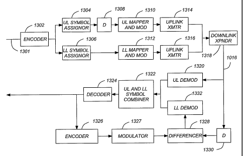
FIGs. 12A and 12B are flow charts describing exemplary operations that can
be used to transmit and receive layered modulation signals. FIG. 12A describes
exemplary transmission operations while FIG. 12B describes exemplary reception
operations. FIGs. 12A and 12B will be discussed in further reference to FIG.
13 and
FIG. 14. FIG. 13 presents a block diagram of salient elements of a
representative
transmitter and receiver that can perform the operations described in FIGs.
12A and
12B, while FIG. 14 presents a diagram showing the timing relationship of the
UL and
LL signals.
Referring first to FIG. 12A, the upper layer signal and lower layer signal are
combined to form an input signal 1301, as shown in block 1202. In block 1204,
the
combined upper layer and lower layer signals are encoded. This can be
accomplished,
for example, using the encoder shown in FIG. 13. Next, symbols are assigned to
the
encoded upper and lower layer signals. This can be accomplished by the UL
symbol
assignor 1304 and the LL symbol assignor 1306. The UL signal, in the form of
UL
symbols, is then delayed by delay element 1308. This is shown in block 1206.
As
will become clear, the upper layer signal is delayed by an amount of time
necessary
for a receiver of the transmitted coded signal to remodulate and re-encode a
demodulated upper layer signal so that the lower layer signal can be
incoherently
demodulated.
The upper layer signal is then mapped to the desired constellation and
modulated by mapper/modulator 1310. Similarly, the lower layer signal is
mapped
and modulated by mapper modulator 1312. This is shown in blocks 1208 and 1210.
24
CA 02503530 2005-04-22
WO 2004/040403 PCT/US2003/032264
The modulated upper layer and lower layer signals are uplinked from the uplink
center
104 via uplink transmitters 1314, 1316, uplink 116, and downlinked to an IRD
500 at
the receiving station 110 via downlink transponder 1318 and downlink 118.
FIG. 12B presents exemplary steps that can be used to receive, demodulate,
and decode the transmitted signal. The transmitted signal is demodulated to
produce
the upper layer signal, as shown in block 1212. This can be performed by the
upper
layer demodulator 1320 shown in FIG. 13. The input signal is then delayed, as
shown
in block 1214. This can be performed by the delay element 1330. The delayed
input
signal is then demodulated to produce the lower layer signal, as shown in
block 1216.
The input signal is demodulated by extracting the lower layer signal from the
upper layer signal with differencer 1328. The upper layer signal is
reconstituted by re-
encoding and'remodulating the upper layer signal demodulated and decoded by
the
upper layer demodulator 1320 and decoder 1324. This is accomplished by the
encoder 1326, and the modulator 1327.
Delay element 1330 delays the lower layer signal in an amount approximately
equivalent to the ainount that the upper layer signal was delayed by block
1308. The
use of delay elements 1308 and 1330 accounts for the time required to re-
encode,
remodulate the upper layer signal and extract the lower layer signal.
FIG. 14A is a diagram showing the relative timing of the upper layer signal
and the lower layer signal. Blocks 1401 of the combined upper layer signal at
succeeding periods of time (denoted U 1, U2 ,==, UN ) are encoded according to
a
Ll L2 LN
coding period T to produce data stream 1402. The upper layer signal Ul, U2,
===, UN
is delayed before being modulated, uplinked, and downlinked, so the received
data
stream becomes Uo , Ul UN-1 The upper layer signal is then demodulated,
Ll L2 LN
producing data stream 1406. This upper layer signal is decoded, re-encoded,
and
modulated by the decoder 1324, encoder 1326 and modulator 1327, and provided
to
CA 02503530 2005-04-22
WO 2004/040403 PCT/US2003/032264
the differencer 1328 to extract the lower level signal. Since the lower layer
signal is
delayed by delay element 1330, the tiining relationship_of the demodulated
upper and
lower level signals is as shown in data stream 1408, with the upper and lower
level
signals once again in a proper timing relationship.
Since the decoded upper layer signal is used to demodulate and decode the
lower layer as well, the above operations require that the upper layer signal
must be
decodable in its own right from the encoded combined upper and lower layer
signals.
To achieve this, timing data such as initialization blocks (1B) having known,
predetermined lower layer data can be inserted into at least some of the
signal blocks
U Ll 1,UL2 2 ,==, LN UN . These IBs can be inserted periodically or
aperiodically. The lower
layer demodulator 1332 can also search for these blocks for timing and
synchronization purposes as well.
The inclusion of IBs decreases the throughput by a small amount. For
example, if the IBs include a 10K block of data and the data is transinitted
at a 25MHz
rate, each block would be approximately 0.5 milliseconds in lengtli,
transmitted every
25milliseconds. This indicates that including the IBs results in a 2%
reduction in
throughput.
FIG. 14B is a diagram presenting the timing relationship of the UL and LL
signals in another embodiment of the present invention. In this embodiment,
the
majority of the blocks 1401 are as was described in FIG. 14A. However, some of
portion of the upper layer signal and the lower layer signal are separately
encoded,
producing separate blocks 1418, 1420 of data. Separately encoded data blocks
having
timing data in the form of IBs can be inserted from time-to-time in the data
stream
1410, either periodically or aperiodically. Since the upper layer signal is
separately
encoded from the lower layer signal, the upper layer signal is decodable by
itself, and
does not require known lower layer data to be inserted in the IBs as was the
case with
the embodiment illustrated in FIG. 14A. In one embodiment, for uniformity in
block
26
CA 02503530 2008-08-05
timing, the IB codeword length is 1/2 that of the codeword described in FIG.
14A.
Since the codeword for the upper layer data and the lower layer data is
smaller than
was the case in the embodiment illustrated in FIG. 14A, this embodiment can
result in
slightly greater errors, but the code rate may be reduced to account for the
smaller
codeword, if desired. Unlike the embodiment shown in FIG. 14A, this embodiment
assures that both the upper layer signal and the lower layer signal carry
payload to
maximize spectral throughput.
FIGs. 15A and 15B are diagrams showing illustrative process steps that can be
used to practice another embodiment of the invention. FIGs. 15A and 15B are
discussed in concert with FIGs. 16 and 17. FIG. 16 presents a block diagram of
salient elements of a representative transmitter and receiver that can perform
the
operations described in FIGs. 15A and 15B. In this embodiment, the upper layer
signal and the lower layer signal are separately and multiplexingly encoded,
as shown
in block 1502. This can be accomplished by using multiplexer 1604 to apply the
upper layer signal and the lower layer signal to a single encoder such as
encoder 1302
shown in FIG 16. As before, upper layer and lower layer symbols are assigned,
and
the upper layer, and the upper layer signal and the lower layer signal is
mapped and
modulated, as shown in blocks 1504 and 1506. This can be accomplished, for
example, by mapper/modulators 1310 and 1312. The result is transmitted, as
shown
in blocks 1508 and 1510. This can be accomplished by uplink transmitters 1314
and
downlink transponder 1318.
Turning to FIG. 15B, the received coded input signal is demodulated to
produce a coded upper layer signal and a coded lower layer signal. This is
shown in
blocks 1512 and 1514. These demodulation steps can be performed, for example,
by
demodulators 1320 and 1322. The coded upper layer signal and the coded lower
layer
signal are then multiplexingly decoded, as shown in block 1516. This can be
performed, for example, by alternatively using the switch 1602 or multiplexer
to apply
the demodulated coded signals to the decoder 1324.
27
CA 02503530 2005-04-22
WO 2004/040403 PCT/US2003/032264
In this embodiment, the same code can be used for the upper and lower layer
signals, and a single decoder 1324 in the IRD 500 is multiplexed between the
upper
layer and lower layer signals, preferably with a 1/ 2 duty cycle. Also, this
embodiment includes buffer storage for decoding in the amount of 3/4 of a
block for
upper layer 4-bit symbols, and one block for lower layer symbols.
This process is illustrated in FIG. 17, which shows representative data
streams
from the foregoing processes. Data stream 1702 shows the upper and lower layer
signals arriving at the receiver. The upper and lower layer signals arrive in
separate
blocks 1704 and 1708, each of which were separately encoded by the encoder
1302.
The upper layer signal is simply demodulated, resulting in data stream 1710.
The
upper layer signal is then decoded. Since the upper layer signal was
separately
encoded, this is possible to achieve with the upper layer signal alone. The
decoded
upper layer signal is then remodulated and re-encoded, resulting in data
stream 1712.
The result is used to demodulate the lower layer, with the results shown in
data stream
1714. The demodulated upper and lower layers are at this point, interleaved
with one
another, and are provided to the decoder 1324. The results can be de-
interleaved by a
de-interleaver and can be applied to a Reed-Solomon or similar decoder as
well.
The layered modulation (LM) technique described above typically requires the
use of satellite transponders 108A, 108B having greater power output than
those
associated with ordinary modulation techniques. Typically, the upper signal
layer 402
must be modulated by a carrier of substantially higher power than the lower
signal
layer 420. Also, backwards compatible (BWC) applications typically require
more
power than non-BWC applications for the upper signal layer 402.
Conclusion
This concludes the description of the preferred embodiments of the present
invention. The foregoing description of the preferred embodiment of the
invention
has been presented for the purposes of illustration and description. It is not
intended
28
CA 02503530 2005-04-22
WO 2004/040403 PCT/US2003/032264
to be exhaustive or to limit the invention to the precise form disclosed. Many
modifications and variations are possible in light of the above teaching. For
example,
it is noted that the uplink configurations depicted and described in the
foregoing
disclosure can be implemented by one or more hardware modules, one or more
software modules defining instructions performed by a processor, or a
combination of
both.
It is intended that the scope of the invention be limited not by this detailed
description, but rather by the claims appended hereto. The above
specification,
examples and data provide a complete description of the manufacture and use of
the
composition of the invention. Since many embodiments of the invention can be
made
without departing from the spirit and scope of the invention, the invention
resides in
the claims hereinafter appended.
29