Note: Descriptions are shown in the official language in which they were submitted.
CA 02503532 2009-01-30
ESTIMATING THE OPERATING POINT ON A NONLINEAR TRAVELING
WAVE TUBE AMPLIFIER
BACKGROUND OF THE INVENTION
1. Field of the Invention
[0001-00071 The present invention relates to systems and methods for
transmitting
data, and in particular to a system and method for estimating a traveling wave
tube
amplifier operating point to accurately reproduce transmitted signals.
1
CA 02503532 2005-04-22
WO 2004/040406 PCT/US2003/033130
2. Description of the Related Art
[0008] Digital signal communication systems have been used in various fields,
including digital TV signal transmission, either terrestrial or satellite. As
the various
digital signal communication systems and services evolve, there is a
burgeoning
demand for increased data throughput and added services. However, it is more
difficult to implement either improvement in old systems or new services when
it is
necessary to replace existing legacy hardware, such as transmitters and
receivers.
New systems and services are advantaged when they can utilize existing legacy
hardware. In the realm of wireless communications, this principle is further
highlighted by the limited availability of electromagnetic spectrum. Thus, it
is not
possible (or at least not practical) to merely transmit enhanced or additional
data at a
new frequency.
[0009] The conventional method of increasing spectral capacity is to move to a
higher-order modulation, such as from quadrature phase shift keying (QPSK) to
eight
phase shift keying (8PSK) or sixteen quadrature amplitude modulation (16QAM).
Unfortunately, QPSK receivers cannot demodulate conventional 8PSK or 16QAM
signals. As a result, legacy customers with QPSK receivers must upgrade their
receivers in order to continue to receive any signals transmitted with an 8PSK
or
16QAM modulation.
[0010] It is advantageous for systems and methods of transmitting signals to
accommodate enhanced and increased data throughput without requiring
additional
frequency. In addition, it is advantageous for enhanced and increased
throughput
signals for new receivers to be backwards compatible with legacy receivers.
There is
further an advantage for systems and methods which allow transmission signals
to be
upgraded from a source separate from the legacy transmitter.
[0011] It has been proposed that a layered modulation signal, transmitting non-
coherently both upper and lower layer signals, can be employed to meet these
needs.
2
CA 02503532 2005-04-22
WO 2004/040406 PCT/US2003/033130
Such layered modulation systems allow higher information throughput with
backwards compatibility. However, even when backward compatibility is not
required (such as with an entirely new system), layered modulation can still
be
advantageous because it requires a traveling wave tube amplifier (TWTA) peak
power
significantly lower than that for a conventional 8PSK or 16QAM modulation
format
for a given throughput.
[00121 To provide a layered modulation scheme (as described in detail below),
a
reconstructed upper layer signal is subtracted from a received composite
signal to
reveal a lower layer signal. As such, the lower-layer signal performance is
impacted
by how closely the upper-layer signal can be reconstructed relative to the
original
signal. In other words, the lower layer signal performance is impacted by the
fidelity
of the reconstructed signal. Thus, layered modulation requires clean
cancellation of
the upper-layer signal to expose the lower-layer signal for further
processing. Clean
cancellation requires TWTA non-linearity/distortion to be accurately
reproduced in
the reconstruction of the upper-layer signal. Accurate reproduction of TWTA
non-
linearity in turn requires knowledge about the TWTA operating point. However,
such
an accurate reproduction and knowledge of the operating point presents a
significant
roadblock.
[00131 With a TWTA, there is a region of approximate linearity, in which the
output
power is nearly proportional to the input power, followed by a curved
transition to a
point where the output power levels off and reaches a maximum. At this point
(i.e.,
when the TWTA curve becomes non-linear), the amplifier is said to have reached
saturation. Due to this non-linearity and to avoid intermodulation, the input
power is
often "backed off"by a particular amount (e.g., 6 dB). The resulting point on
the
curve after the input power is "backed off' is referred to as the operating
point of the
TWTA. When subsequently reconstructing the upper layer signal, the amount of
distortion/non-linearity used to create the original signal serves to increase
the fidelity
of the reconstructed signal. Thus, to produce a high fidelity reconstructed
upper layer
3
CA 02503532 2005-04-22
WO 2004/040406 PCT/US2003/033130
signal, knowledge of the non-linearity as well as the operating point is
useful.
Accordingly, the inclusion of (or taking into account) TWTA non-linearity (and
operating point) may improve upper-layer signal cancellation ratio by 10 dB or
more
(i.e., the ratio between non-linearity-induced noise before and after
cancellation is
improved).
[0014] Errors in the estimation of the operating point can have a significant
impact
when reconstructing the upper layer-signal. The impact of amplitude (AM-AM
[amplitude modulation to amplitude modulation]) and phase (AM-PM [amplitude
modulation to phase modulation]) operating point errors may be individually
analyzed
based on shift analysis. Individual impacts may then be combined for total
impact.
To evaluate performance impacts, the synthesis of a layer-modulated signal
with
known TWTA non-linearity and system/representative operating CNR (carrier to
noise ratio) may be used. The upper-layer cancellation error may then be
calculated
for each amount of simulated operating point error in the signal
reconstruction
process. Thus, the upper layer cancellation ratio may be plotted against the
operating
point displacement. The cancellation error can then be converted into an
amount of
lower-layer CNR degradation, which increases the CNR required for signals of
both
upper and lower layers. Such an increased CNR illustrates the significance of
operating point estimation errors.
[0015] FIGs. 16A and 16B illustrate the impact of operating point errors in
signal
reconstruction. In FIGs. 16A and 16B, the sensitivity of signal reconstruction
error is
plotted against the TWTA input operating point error. The effective noise is
calculated as a measure of signal reconstruction error.
[0016] In FIG. 16A, a set of generic TWTA non-linearity curves are used. The
signal reconstruction process is assumed to have full knowledge about the non-
linearity curves but is otherwise uncertain about the operating point. The
performance
plots of FIG. 16A indicate that cancellation errors are below -25 dB for an
input
operating point error up to about +/- 1 dB.
4
CA 02503532 2005-04-22
WO 2004/040406 PCT/US2003/033130
[0017] In FIG. 16B, the performance plots are based on the same TWTA non-
linearity but with an input backoff of 8 dB. With such an input backoff, there
is
improved linearity, that is less susceptible to TWTA operating point error. As
a
result, reconstruction and cancellation errors are greatly reduced as
indicated in FIG.
16B. The effective noise is below -33 dB with an input operating error up to
about
+/- 1 dB.
[0018] Accordingly, there is a need for systems and methods for implementing
layered modulation systems that accurately determine TWTA non-linearity and
the
operating point.
[0019] In the prior art, the TWTA operating point is obtained from telemetry
tracking and control (TT&C) commands that set the operating point of the TWTA
(assuming that TWTA characteristics have little changed since the satellite
was
launched). In other words, the operating point set by TT&C commands during pre-
launch measurements is used post-launch after receiving the signals from the
satellite.
However, TWTA characteristics including the non-linearity and operating point
may
change over time (including after satellite launch).
[0020] Accordingly, what is needed is a system and method for accurately
determining the non-linearity and operating point of a TWTA as it changes over
time.
The present invention meets this need and provides further advantages as
detailed
hereafter.
SUMMARY OF THE INVENTION
[0021] To address the requirements described above, the present invention
discloses
a method and apparatus for measuring and applying the non-linearity of a
traveling
wave tube amplifier, such as in satellite communications involving layered
modulation. estimating the operating point on a non-linear traveling wave tube
amplifier (TWTA). In this regard, the invention aids in the accurate
extraction of a
lower-layer signal in a layered modulation scheme. Such an accurate extraction
5
CA 02503532 2005-04-22
WO 2004/040406 PCT/US2003/033130
minimizes the amounts of power required for both layers of a signal and also
helps to
monitor the health of a TWTA.
[0022] To measure/apply the non-linearity of the TWTA, the operating points
(input
and/or output) for the TWTA are also determined. Initially, the non-linearity
of the
TWTA is measured (e.g., using a measuring module). For example, the TWTA non-
linearity maybe measured at a local receiver, or at a broadcast center (in
which case,
the non-linearity is downloaded to a local receiver [ e.g., for layered
modulation and
other applications]). As part of such a non-linearity measurement, various
input and
output values/points are processed to create the non-linearity curve. An input
root-
mean-square (RMS) value of the input signals used to measure the non-linearity
is
computed. The RMS value identifies an input operating point of the measured
non-
linearity of the TWTA. In addition, an output operating point may also be
obtained
(e.g., by a measuring module). The output operating point may be based on an
RMS
value of the various output values/points used in measuring the TWTA non-
linearity.
Alternatively, the output operating point may simply be based on the
corresponding
point (to the input RMS value) on the TWTA non-linearity curve.
[0023] Once the non-linearity has been measured and operating points
obtained/computed, an upper layer signal (as part of the layered modulation
scheme)
may be reconstructed (e.g., by the receiver). Such a reconstruction is more
accurate
since the appropriate levels of distortion accountable to the TWTA non-
linearity are
accounted for. In addition, the measured non-linearity may be offset to
simplify the
reconstruction of the upper signal. Such an offsetting may provide for scaling
an
input amplitude value and output amplitude value of the measured non-linearity
to
place the output operating point at a desired point. Such a scaling may be
conducted
by subtracting a measured input operating point value from all input values in
a log
domain. Accordingly, the scaling may also be conducted by subtracting a
measured
output operating point value from all operating values in the log domain. The
scaling
may also be conducted by subtracting a measured phase value at the output
operating
6
CA 02503532 2009-01-30
point from phase values of all output points used to measure the non-linearity
of the
TWTA.
[0024] In addition to the above, when offsetting the measured non-linearity,
certain
data may fall outside of the measured non-linearity. To account for such data,
bounding points may be placed beyond the end points (that are used to measure
the
non-linearity). Such bounding points may then be used to interpolate data.
Further,
the input operating point and output operating point may also be mapped to a
particular level to avoid fractional overflow.
[0024a] In accordance with one aspect of the present invention, there is
provided a
method for determining an input operating point and an output operating point
on a
non-linear traveling wave tube amplifier (TWTA), comprising:
measuring non-linearity of the TWTA at a given time;
computing an input root-mean-square (RMS) value of an input signal used to
measure the non-linearity of the TWTA, wherein the RMS value identifies an
input
operating point of the measured non-linearity of the TWTA and wherein the
input
RMS value is computed at the same given time of the TWTA non-linearity
measurement; and
obtaining an output operating point.
[0024b] In accordance with another aspect of the present invention, there is
provided
an apparatus for determining an input operating point and an output operating
point
on a non-linear traveling wave tube amplifier (TWTA), comprising:
means for measuring non-linearity of the TWTA at a given time;
means for computing an input root-mean-square (RMS) value of an input
signal used to measure the non-linearity of the TWTA, wherein the RMS value
identifies an input operating point of the measured non-linearity of the TWTA
and
wherein the input value is computed at the same given time of the TWTA non-
linearity measurement; and
means for obtaining an output operating point.
7
CA 02503532 2009-01-30
[0024c] In accordance with a further aspect of the present invention, there is
provided a system for determining an input operating point and an output
operating
point on a non-linear traveling wave tube amplifier (TWTA), comprising:
(a) a measuring module configured to:
(1) measure non-linearity of the TWTA at a given time; and
(2) obtain an output operating point; and
(b) a non-linear distortion map module configured to compute an input
root-mean-square (RMS) value of an input signal used to measure the non-
linearity of
the TWTA, wherein the input RMS value identifies an input operating point of
the
measured non-linearity of the TWTA and wherein the input RMS value is computed
at the same given time of the TWTA non-linearity measurement.
BRIEF DESCRIPTION OF THE DRAWINGS
[0025] Referring now to the drawings in which like reference numbers represent
corresponding parts throughout:
[0026] FIG. 1 is a diagram illustrating an overview of a single satellite
video
distribution system;
[0027] FIG. 2 is a block diagram showing a typical uplink configuration for a
single
satellite transponder;
[0028] FIG. 3A is a diagram of a representative data stream;
[0029] FIG. 3B is a diagram of a representative data packet;
[0030] FIG. 4 is a block diagram showing one embodiment of the modulator for
the
uplink signal;
[0031] FIG. 5 is a block diagram of an integrated receiver/decoder;
[0032] FIGs. 6A - 6C are diagrams illustrating the basic relationship of
signal layers
in a layered modulation transmission;
[0033] FIGs. 7A-7C are diagrams illustrating a signal constellation of a
second
transmission layer over the first transmission layer after first layer
demodulation;
[0034] FIG. 8A is a diagram showing a system for transmitting and receiving
layered modulation signals;
7a
CA 02503532 2005-04-22
WO 2004/040406 PCT/US2003/033130
[0035] FIG. 8B is a diagram showing an exemplary satellite transponder for
receiving and transmitting layered modulation signals;
[0036] FIG. 9 is a block diagram depicting one embodiment of an enhanced IRD
capable of receiving layered modulation signals;
[0037] FIG. I OA is a block diagram of one embodiment of the enhanced
tuner/modulator and FEC encoder;
[0038] FIG. 10B depicts another embodiment of the enhanced tuner/modulator
wherein layer subtraction is performed on the received layered signal;
[0039] FIGS. 1 1A and 11B depict the relative power levels of example
embodiments of the present invention;
[0040] FIG. 12 illustrates an exemplary computer system that could be used to
implement selected modules or functions the present invention;
[0041] FIG. 13 is a flow chart illustrating the determination of the operating
point in
accordance with one or more embodiments of the invention;
[0042] FIGS. 14A and 14B are block diagrams of a basic system for measuring
performance maps in accordance with one or more embodiments of the invention;
[0043] FIG. 14C is a flowchart illustrating a method for measuring performance
maps in accordance with one or more embodiments of the invention;
[0044] FIG. 15A illustrates an intuitive algorithm for obtaining the output in-
phase
and quadrature components in accordance with one or more embodiments of the
invention;
[0045] FIG. 15 B illustrates a computationally efficient algorithm for
obtaining the
input and output operating points in accordance with one or more embodiments
of the
invention; and
[0046] FIGs. 16A and 16B illustrate the impact of operating point errors in
signal
reconstruction.
8
CA 02503532 2005-04-22
WO 2004/040406 PCT/US2003/033130
DETAILED DESCRIPTION OF PREFERRED EMBODIMENTS
[0047] In the following description, reference is made to the accompanying
drawings which form a part hereof, and which is shown, by way of illustration,
several
embodiments of the present invention. It is understood that other embodiments
may
be utilized and structural changes may be made without departing from the
scope of
the present invention.
1. Overview
[0048] The invention provides a method of determining/estimating the operating
point of a TWTA. The operating point is estimated at the same time TWTA non-
linearity is measured. Therefore, no extra measurement procedures are required
for
the determination of the operating point, and the measured non-linearity is
always up-
to-date, allowing the measurement to follow any changes in TWTA
characteristics
over time.
2. Video Distribution System
[0049] FIG. 1 is a diagram illustrating an overview of a single satellite
video
distribution system 100. The video distribution system 100 comprises a control
center
102 in communication with an uplink center 104 via a ground or other link 114
and
with a subscriber receiver station 110 via a public switched telephone network
(PSTN) or other link 120. The control center 102 provides program material
(e.g.
video programs, audio programs and data) to the uplink center 104 and
coordinates
with the subscriber receiver stations 110 to offer, for example, pay-per-view
(PPV)
program services, including billing and associated decryption of video
programs.
[0050] The uplink center 104 receives program material and program control
information from the control center 102, and using an uplink antenna 106 and
transmitter 105, transmits the program material and program control
information to
the satellite 108 via uplink signal 116. The satellite receives and processes
this
9
CA 02503532 2005-04-22
WO 2004/040406 PCT/US2003/033130
information, and transmits the video programs and control information to the
subscriber receiver station 110 via downlink signal 118 using transmitter 107.
The
subscriber receiving station 110 receives this information using the outdoor
unit
(ODU) 112, which includes a subscriber antenna and a low noise block converter
(LNB).
[0051] In one embodiment, the subscriber receiving station antenna is an 18-
inch
slightly oval-shaped Ku-band antenna. The slight oval shape is due to the 22.5
degree
offset feed of the LNB (low noise block converter) which is used to receive
signals
reflected from the subscriber antenna. The offset feed positions the LNB out
of the
way so it does not block any surface area of the antenna minimizing
attenuation of the
incoming microwave signal.
[0052] The video distribution system 100 can comprise a plurality of
satellites 108
in order to provide wider terrestrial coverage, to provide additional
channels, or to
provide additional bandwidth per channel. In one embodiment of the invention,
each
satellite comprises 16 transponders to receive and transmit program material
and other
control data from the uplink center 104 and provide it to the subscriber
receiving
stations 110. Using data compression and multiplexing techniques the channel
capabilities, two satellites 108 working together can receive and broadcast
over 150
conventional (non-HDTV) audio and video channels via 32 transponders.
[0053] While the invention disclosed herein will be described with reference
to a
satellite-based video distribution system 100, the present invention may also
be
practiced with terrestrial-based transmission of program information, whether
by
broadcasting means, cable, or other means. Further, the different functions
collectively allocated among the control center 102 and the uplink center 104
as
described above can be reallocated as desired without departing from the
intended
scope of the present invention.
[0054] Although the foregoing has been described with respect to an embodiment
in
which the program material delivered to the subscriber 122 is video (and
audio)
CA 02503532 2005-04-22
WO 2004/040406 PCT/US2003/033130
program material such as a movie, the foregoing method can be used to deliver
program material comprising purely audio information or other data as well.
2.1 Uplink Configuration
[0055] FIG. 2 is a block diagram showing a typical uplink configuration for a
single
satellite 108 transponder, showing how video program material is uplinked to
the
satellite 108 by the control center 102 and the uplink center 104. FIG. 2
shows three
video channels (which may be augmented respectively with one or more audio
channels for high fidelity music, soundtrack information, or a secondary audio
program for transmitting foreign languages), a data channel from a program
guide
subsystem 206 and computer data information from a computer data source 208.
[0056] The video channels are provided by a program source 200A-200C of video
material (collectively referred to hereinafter as program source(s) 200). The
data from
each program source 200 is provided to an encoder 202A-202C (collectively
referred
to hereinafter as encoder(s) 202). Each of the encoders accepts a program time
stamp
(PTS) from the controller 216. The PTS is a wrap-around binary time stamp that
is
used to assure that the video information is properly synchronized with the
audio
information after encoding and decoding. A PTS time stamp is sent with each I-
frame
of the MPEG encoded data.
[0057] In one embodiment of the present invention, each encoder 202 is a
second
generation Motion Picture Experts Group (MPEG-2) encoder, but other decoders
implementing other coding techniques can be used as well. The data channel can
be
subjected to a similar compression scheme by an encoder (not shown), but such
compression is usually either unnecessary, or performed by computer programs
in the
computer data source (for example, photographic data is typically compressed
into
*.TIF files or *.JPG files before transmission). After encoding by the
encoders 202,
the signals are converted into data packets by a packetizer 204A-204F
(collectively
referred to hereinafter as packetizer(s) 204) associated with each program
source 200.
11
CA 02503532 2005-04-22
WO 2004/040406 PCT/US2003/033130
[0058] The data packets are assembled using a reference from the system clock
214
(SCR), and from the conditional access manager 210, which provides the service
channel identifier (SCID) to the packetizers 204 for use in generating the
data packets.
These data packets are then multiplexed into serial data and transmitted.
2.2 Broadcast Data Stream Format and Protocol
[0059] FIG. 3A is a diagram of a representative data stream. The first packet
segment 302 comprises information from video channel 1 (data coming from, for
example, the first video program source 200A). The next packet segment 304
comprises computer data information that was obtained, for example from the
computer data source 208. The next packet segment 306 comprises information
from
video channel 5 (from one of the video program sources 200). The next packet
segment 308 comprises program guide information such as the information
provided
by the program guide subsystem 206. As shown in FIG. 3A, null packets 310
created
by the null packet module 212 may be inserted into the data stream as desired
followed by further data packets 312, 314, 316 from the program sources 200.
[0060] The data stream therefore comprises a series of packets(302-316) from
any
one of the data sources(e.g. program sources 200, program guide subsystem 206,
computer data source 208) in an order determined by the controller 216. The
data
stream is encrypted by the encryption module 218, modulated by the modulator
220
(typically using a QPSK modulation scheme), and provided to the transmitter
105/222, which broadcasts the modulated data stream on a frequency bandwidth
to the
satellite via the antenna 106. The receiver 500 at the receiver station 110
receives
these signals, and using the SCID, reassembles the packets to regenerate the
program
material for each of the channels.
[0061] FIG. 3B is a diagram of a data packet. Each data packet (e.g. 302-316)
is
147 bytes long, and comprises a number of packet segments. The first packet
segment
320 comprises two bytes of information containing the SCID and flags. The SCID
is a
12
CA 02503532 2005-04-22
WO 2004/040406 PCT/US2003/033130
unique 12-bit number that uniquely identifies the data packet's data channel.
The
flags include 4 bits that are used to control other features. The second
packet segment
322 is made up of a 4-bit packet type indicator and a 4 -bit continuity
counter. The
packet type identifies the packet as one of the four data types (video, audio,
data, or
null). When combined with the SCID, the packet type determines how the data
packet
will be used. The continuity counter increments once for each packet type and
SCID.
The next packet segment 324 comprises 127 bytes of payload data, which in the
cases
of packets 302 or 306 is a portion of the video program provided by the video
program source 200. The final packet segment 326 is data required to perform
forward error correction.
[0062] FIG. 4 is a block diagram showing one embodiment of the modulator 220.
The modulator 220 optionally comprises a forward error correction (FEC)
encoder
404 which accepts the first signal symbols 402 and adds redundant information
that
are used to reduce transmission errors. The coded symbols 405 are modulated by
modulator 406 according to a first carrier 408 to produce an upper layer
modulated
signal 410. Second symbols 420 are likewise provided to an optional second FEC
encoder 422 to produce coded second symbols 424. The coded second symbols 424
are provided to a second modulator 414, which modulates the coded second
symbols
424 according to a second carrier 416 to produce a lower layer modulated
signal 418.
The upper layer modulated signal 410 and the lower layer modulated signal 418
are
therefore uncorrelated. Thus, the upper layer signal 410 and the lower layer
signal
418 can be transmitted to separate transponders on one or more satellites 108
via
separate uplink signals 116. Thus, the lower layer signal 418 can be
implemented
from a separate satellite 108 that receives a separate uplink signal 116.
However, in
the downlink signal 118 the upper layer signal 410, must be a sufficiently
greater
amplitude signal than the lower layer signal 418, to maintain the signal
constellations
shown in FIG. 6 and FIG. 7.
13
CA 02503532 2005-04-22
WO 2004/040406 PCT/US2003/033130
[0063] It should be noted that it may be more efficient to retrofit an
existing system
by using a transponder on a separate satellite 108 to transmit the lower layer
downlink
signal over the existing legacy downlink signal rather than replacing the
legacy
satellite with one that will transmit both downlink signal layers. Emphasis
can be
given to accommodating the downlink legacy signal in implementing a layered
downlink broadcast.
2.3 Integrated Receiver/Decoder
[0064] FIG. 5 is a block diagram of an integrated receiver/decoder (IRD) 500
(also
hereinafter alternatively referred to as receiver 500). The receiver 500
comprises a
tuner/demodulator 504 communicatively coupled to an ODU 112 having one or more
low noise blocks (LNBs) 502. The LNB 502 converts the 12.2- to 12.7 GHz
downlink 118 signal from the satellites 108 to, e.g., a 950-1450 MHz signal
required
by the IRD's 500 tuner/demodulator 504. Typically, the LNB 502 may provide
either
a dual or a single output. The single-output LNB 502 has only one RF
connector,
while the dual output LNB 502 has two RF output connectors and can be used to
feed
a second tuner 504, a second receiver 500, or some other forin of distribution
system.
[0065] The tuner/demodulator 504 isolates a single, digitally modulated 24 MHz
transponder signal, and converts the modulated data to a digital data stream.
Further
details regarding the demodulation of the received signal follow.
[0066] The digital data stream is then supplied to a forward error correction
(FEC)
decoder 506. This allows the IRD 500 to reassemble the data transmitted by the
uplink center 104 (which applied the forward error correction to the desired
signal
before transmission to the subscriber receiving station 110) verifying that
the correct
data signal was received, and correcting errors, if any. The error-corrected
data may
be fed from the FEC decoder module 506 to the transport module 508 via an 8-
bit
parallel interface.
14
CA 02503532 2005-04-22
WO 2004/040406 PCT/US2003/033130
[0067] The transport module 508 performs many of the data processing functions
performed by the IRD 500. The transport module 508 processes data received
from
the FEC decoder module 506 and provides the processed data to the video MPEG
decoder 514 and the audio MPEG decoder 517. As needed the transport module
employs system RAM 528 to process the data. In one embodiment of the present
invention, the transport module 508, video MPEG decoder514 and audio MPEG
decoder 517 are all implemented on integrated circuits. This design promotes
both
space and power efficiency, and increases the security of the functions
performed
within the transport module 508. The transport module 508 also provides a
passage
for communications between the microcontroller 510 and the video and audio
MPEG
decoders 514, 517. As set forth more fully hereinafter, the transport module
also
works with the conditional access module (CAM) 512 to determine whether the
subscriber receiving station 110 is permitted to access certain program
material. Data
from the transport module 508 can also be supplied to external communication
module 526.
[0068] The CAM 512 functions in association with other elements to decode an
encrypted signal from the transport module 508. The CAM 512 may also be used
for
tracking and billing these services. In one embodiment of the present
invention, the
CAM 512 is a removable smart card, having contacts cooperatively interacting
with
contacts in the IRD 500 to pass information. In order to implement the
processing
performed in the CAM 512, the IRD 500, and specifically the transport module
508
provides a clock signal to the CAM 512.
[0069] Video data is processed by the MPEG video decoder 514. Using the video
random access memory (RAM) 536, the MPEG video decoder 514 decodes the
compressed video data and sends it to an encoder or video processor 516, which
converts the digital video information received from the video MPEG module 514
into an output signal usable by a display or other output device. By way of
example,
processor 516 may comprise a National TV Standards Committee (NTSC) or
CA 02503532 2010-02-12
Advanced Television Systems Committee (ATSC) encoder. In one embodiment of
the invention both S-Video and ordinary video (NTSC or ATSC) signals are
provided.
Other outputs may also be utilized, and are advantageous if high definition
programming is processed.
[00701 Audio data is likewise decoded by the MPEG audio decoder 517. The
decoded audio data may then be sent to a digital to analog (D/A) converter
518. In
one embodiment of the present invention, the D/A converter 518 is a dual D/A
converter, one for the right and left channels. If desired, additional
channels can be
added for use in surround sound processing or secondary audio programs (SAPs).
In
one embodiment of the invention, the dual D/A converter 518 itself separates
the left
and right channel information, as well as any additional channel information.
Other
audio formats may similarly be supported. For example, other audio formats
such as
multi-channel DOLBY DIGITALTM AC-3 may be supported.
100711 A description of the processes performed in the encoding and decoding
of
video streams, particularly with respect to MPEG and JPEG encoding/decoding,
can
be found in Chapter 8 of "Digital Television Fundamentals," by Michael Robin
and
Michel Poulin, McGraw-Hill, 1998.
[00721 The microcontroller 510 receives and processes command signals from the
remote control 524, an IRD 500 keyboard interface, and/or another input
device. The
microcontroller 510 receives commands for performing its operations from a
processor programming memory, which permanently stores such instructions for
performing such commands. The processor programming memory may comprise a
read only memory (ROM) 538, an electrically erasable programmable read only
memory (EEPROM) 522 or, similar memory device. The microcontroller 510 also
controls the other digital devices of the IRD 500 via address and data lines
(denoted
"A" and "D" respectively, in FIG. 5).
[00731 The modem 540 connects to the customer's phone line via the PSTN port
120. It calls, e. g. the program provider, and transmits the customer's
purchase
16
CA 02503532 2005-04-22
WO 2004/040406 PCT/US2003/033130
information for billing purposes, and/or other information. The modem 540 is
controlled by the microprocessor 510. The modem 540 can output data to other
1/0
port types including standard parallel and serial computer 1/0 ports.
[0074] The present invention also comprises a local storage unit such as the
video
storage device 532 for storing video and/or audio data obtained from the
transport
module 508. Video storage device 532 can be a hard disk drive, a read/writable
compact disc of DVD, a solid state RAM, or any other suitable storage medium.
In
one embodiment of the present invention, the video storage device 532 is a
hard disk
drive with specialized parallel read/write capability so that data may be read
from the
video storage device 532 and written to the device 532 at the same time. To
accomplish this feat, additional buffer memory accessible by the video storage
532 or
its controller may be used. Optionally, a video storage processor 530 can be
used to
manage the storage and retrieval of the video data from the video storage
device 532.
The video storage processor 530 may also comprise memory for buffering data
passing into and out of the video storage device 532. Alternatively or in
combination
with the foregoing, a plurality of video storage devices 532 can be used. Also
alternatively or in combination with the foregoing, the microcontroller 510
can also
perform the operations required to store and or retrieve video and other data
in the
video storage device 532.
[0075] The video processing module 516 input can be directly supplied as a
video
output to a viewing device such as a video or computer monitor. In addition,
the
video and/or audio outputs can be supplied to an RF modulator 534 to produce
an RF
output and/or 8 vestigal side band (VSB) suitable as an input signal to a
conventional
television tuner. This allows the receiver 500 to operate with televisions
without a
video output.
[0076] Each of the satellites 108 comprises a transponder, which accepts
program
information from the uplink center 104, and relays this information to the
subscriber
receiving station 110. Known multiplexing techniques are used so that multiple
17
CA 02503532 2005-04-22
WO 2004/040406 PCT/US2003/033130
channels can be provided to the user. These multiplexing techniques include,
by way
of example, various statistical or other time domain multiplexing techniques
and
polarization multiplexing. In one embodiment of the invention, a single
transponder
operating at a single frequency band carries a plurality of channels
identified by
respective service channel identification (SCID).
[0077] Preferably, the IRD 500 also receives and stores a program guide in a
memory available to the microcontroller 510. Typically, the program guide is
received in one or more data packets in the data stream from the satellite
108. The
program guide can be accessed and searched by the execution of suitable
operation
steps implemented by the microcontroller 510 and stored in the processor ROM
538.
The program guide may include data to map viewer channel numbers to satellite
transponders and service channel identifications (SCIDs), and also provide TV
program listing information to the subscriber 122 identifying program events.
[0078] The functionality implemented in the IRD 500 depicted in FIG. 5 can be
implemented by one or more hardware modules, one or more software modules
defining instructions performed by a processor, or a combination of both.
[0079] The present invention provides for the modulation of signals at
different
power levels and advantageously for the signals to be non-coherent from each
layer.
In addition, independent modulation and coding of the signals may be
performed.
Backwards compatibility with legacy receivers, such as a quadrature phase
shift
keying (QPSK) receiver is enabled and new services are provided to new
receivers. A
typical new receiver of the present invention uses two demodulators and one
remodulator as will be described in detail hereafter.
[0080] In a typical backwards-compatible embodiment of the present invention,
the
legacy QPSK signal is boosted in power to a higher transmission (and
reception)
level. This creates a power "room" in which a new lower layer signal may
operate.
The legacy receiver will not be able to distinguish the new lower layer
signal, from
additive white Gaussian noise, and thus operates in the usual manner. The
optimum
18
CA 02503532 2005-04-22
WO 2004/040406 PCT/US2003/033130
selection of the layer power levels is based on accommodating the legacy
equipment,
as well as the desired new throughput and services.
[0081] The new lower layer signal is provided with a sufficient carrier to
thermal
noise ratio to function properly. The new lower layer signal and the boosted
legacy
signal are non-coherent with respect to each other. Therefore, the new lower
layer
signal can be implemented from a different TWTA and even from a different
satellite.
The new lower layer signal format is also independent of the legacy format,
e.g., it
may be QPSK or 8PSK, using the conventional concatenated FEC code or using a
new Turbo code. The lower layer signal may even be an analog signal.
[0082] The combined layered signal is demodulated and decoded by first
demodulating the upper layer to remove the upper carrier. The stabilized
layered
signal may then have the upper layer FEC decoded and the output upper layer
symbols
communicated to the upper layer transport. The upper layer symbols are also
employed in a remodulator, to generate an idealized upper layer signal. The
idealized
upper layer signal is then subtracted from the stable layered signal to reveal
the lower
layer signal. The lower layer signal is then demodulated and FEC decoded and
communicated to the lower layer transport.
[0083] Signals, systems and methods using the present invention may be used to
supplement a pre-existing transmission compatible with legacy receiving
hardware in
a backwards-compatible application or as part of a preplanned layered
modulation
architecture providing one or more additional layers at a present or at a
later date.
2.4 Layered Signals
[0084] FIGs. 6A - 6C illustrate the basic relationship of signal layers in a
received
layered modulation transmission. FIG. 6A illustrates an upper layer signal
constellation 600 of a transmission signal showing the signal points or
symbols 602.
FIG. 6B illustrates the lower layer signal constellation of symbols 604 over
the upper
layer signal constellation 600 where the layers are coherent (or
synchronized). FIG.
19
CA 02503532 2005-04-22
WO 2004/040406 PCT/US2003/033130
6C illustrates a lower layer signal 606 of a second transmission layer over
the upper
layer constellation where the layers are non-coherent. The lower layer 606
rotates
about the upper layer constellation 602 due to the relative modulating
frequencies of
the two layers in a non-coherent transmission. Both the upper and lower layers
rotate
about the origin due to the first layer modulation frequency as described by
path 608.
[0085] FIGs. 7A - 7C are diagrams illustrating a non-coherent relationship
between
a lower transmission layer over the upper transmission layer after upper layer
demodulation. FIG. 7A shows the constellation 700 before the first carrier
recovery
loop (CRL) of the upper layer and the constellation rings 702 rotate around
the large
radius circle indicated by the dashed line. FIG. 7B shows the constellation
704 after
CRL of the upper layer where the rotation of the constellation rings 702 is
stopped.
The constellation rings 702 are the signal points of the lower layer around
the nodes
602 of the upper layer. FIG. 7C depicts a phase distribution of the received
signal
with respect to nodes 602.
[0086] Relative modulating frequencies of the non-coherent upper and lower
layer
signals cause the lower layer constellation to rotate around the nodes 602 of
the upper
layer constellation to form rings 702. After the lower layer CRL this rotation
is
eliminated and the nodes of the lower layer are revealed (as shown in FIG.
6B). The
radius of the lower layer constellation rings 702 is indicative of the lower
layer power
level. The thickness of the rings 702 is indicative of the carrier to noise
ratio (CNR)
of the lower layer. As the two layers are non-coherent, the lower layer may be
used to
transmit distinct digital or analog signals.
[0087] FIG. 8A is a diagram showing a system for transmitting and receiving
layered modulation signals. Separate transmitters 107A, 107B (that include
TWTAs
to amplify the signals), as may be located on any suitable platform, such as
satellites
108A, 108B, are used to non-coherently transmit different layers of a signal
of the
present invention. Uplink signals 116 are typically transmitted to each
satellite 108A,
CA 02503532 2005-04-22
WO 2004/040406 PCT/US2003/033130
108B from one or moreuplink centers 104 with one or more transmitters 105 via
an
antenna 106.
[0088] FIG. 8B is a diagram illustrating an exemplary satellite transponder
107 for
receiving and transmitting layered modulation signals on a satellite 108. The
uplink
signal 116 is received by the satellite 108 and passed through a input
multiplexer
(IMUX) 814. Following this the signal is amplified with a travelling wave tube
amplifier (TWTA) 816 and then through an output muliplexer (OMUX) 818 before
the downlink signal 118 is transmitted to the receivers 802, 500.
[0089] The layered signals 808A, 808B (e.g. multiple downlink signals 118) are
received at receiver antennas 812A, 812B, such as satellite dishes, each with
a low
noise block (LNB) 81 OA, 81OB where they are then coupled to integrated
receiver/decoders (IRDs) 500, 802. For example, first satellite 108A and
transmitter
107A can transmit an upper layer legacy signal 808A and second satellite 108B
and
transmitter 107B can transmit a lower layer signal 808B. Although both signals
808A, 808B arrive at each antenna 812A, 812B and LNB 810A, 810B, only the
layer
modulation IRD 802 is capable of decoding both signals 808A, 808B. The legacy
receiver 500 is only capable of decoding the upper layer legacy signal 808A;
the lower
layer signal 808B appears only as noise to the legacy receiver 500.
[0090] Because the signal layers maybe transmitted non-coherently, separate
transmission layers may be added at any time using different satellites 108A,
108B or
other suitable platforms, such as ground based or high altitude platforms.
Thus, any
composite signal, including new additional signal layers will be backwards
compatible
with legacy receivers 500, which will disregard the new signal layers. To
ensure that
the signals do not interfere, the combined signal and noise level for the
lower layer
must be at or below the allowed noise floor for the upper layer at the
particular
receiver antenna 812A, 812B.
[0091] Layered modulation applications include backwards compatible and non-
backwards compatible applications. "Backwards compatible" in this sense,
describes
21
CA 02503532 2005-04-22
WO 2004/040406 PCT/US2003/033130
systems in which legacy receivers 500 are not rendered obsolete by the
additional
signal layer(s). Instead, even if the legacy receivers 500 are incapable of
decoding the
additional signal layer(s), they are capable of receiving the layered
modulated signal
and decoding the original signal layer. In these applications, the pre-
existing system
architecture is accommodated by the architecture of the additional signal
layers.
"Non-backwards compatible" describes a system architecture which makes use of
layered modulation, but the modulation scheme employed is such that pre-
existing
equipment is incapable of receiving and decoding the information on additional
signal
layer(s).
[0092] The pre-existing legacy IRDs 500 decode and make use of data only from
the
layer (or layers) they were designed to receive, unaffected by the additional
layers.
However, as will be described hereafter, the legacy signals may be modified to
optimally implement the new layers. The present invention may be applied to
existing
direct satellite services which are broadcast to individual users in order to
enable
additional features and services with new receivers without adversely
affecting legacy
receivers and without requiring additional signal frequency.
2.5 Demodulator and Decoder
[0093] FIG. 9 is a block diagram depicting one embodiment of an enhanced IRD
802 capable of receiving layered modulation signals. The enhanced IRD 802
includes
a feedback path 902 in which the FEC decoded symbols are fed back to a
enhanced
modified tuner/demodulator 904 and transport module 908 for decoding both
signal
layers as detailed hereafter.
[0094] FIG. 10A is a block diagram of one embodiment of the enhanced
tuner/modulator 904 and FEC encoder 506. FIG. 10A depicts reception where
layer
subtraction is performed on a signal where the upperlayer carrier has already
been
demodulated. The upper layer of the received combined signal 1016 from the LNB
502, which may contain legacy modulation format, is provided to and processed
by an
22
CA 02503532 2005-04-22
WO 2004/040406 PCT/US2003/033130
upper layer demodulator 1004 to produce the stable demodulated signal 1020.
The
demodulated signal 1010 is communicatively coupled to a FEC decoder 1002 which
decodes the upper layer to produce the upper layer symbols which are output to
an
upper layer transport module 908. The upper layer symbols are also used to
generate
an idealized upper layer signal. The upper layer symbols may be produced from
the
decoder 402 after Viterbi decode (BER<10-3 or so) or after Reed-Solomon (RS)
decode (BER<10-9 or so), in typical decoding operations known to those skilled
in the
art. The upper layer symbols are provided via feedback path 902 from the upper
layer
decoder 402 to a remodulator 406 which effectively produces an idealized upper
layer
signal. The idealized upper level signal is subtracted from the demodulated
upper
layer signal 1020.
[0095] In order for the subtraction to yield a clean small lower layer signal,
the
upper layer signal must be precisely reproduced. The modulated signal may have
been distorted, for example, by traveling wave tube amplifier (TWTA) non-
linearity
or other non-linear or linear distortions in the transmission channel. The
distortion
effects are estimated from the received signal after the fact or from TWTA
characteristics which may be downloaded into the IRD in AM - AM and/or AM - PM
maps 1014, used to eliminate the distortion (e.g., using the non-linear
distortion map
module 1018) (see detailed description below).
[0096] A subtractor 1012 then subtracts the idealized upper layer signal from
the
stable demodulated signal 1020. This leaves the lower-power second layer
signal.
The subtractor 1012 may include a buffer or delay function to retain the
stable
demodulated signal 1020 while the idealized upper layer signal is being
constructed.
The second layer signal is demodulated by the lower level demodulator 1010 and
FEC
decoded by decoder 1008 according to its signal format to produce the lower
layer
symbols, which are provided to the transport module 908.
[0097] FIG. l OB depicts another embodiment wherein layer subtraction is
performed on the received layered signal (prior to upper layer demodulation).
In this
23
CA 02503532 2005-04-22
WO 2004/040406 PCT/US2003/033130
case, the upper layer demodulator 1004 produces the upper carrier signal 1022
(as
well as the stable demodulated signal output 1020). An upper carrier signal
1022 is
provided to the remodulator 1006. The remodulator 1006 provides the
remodulated
signal to the non-linear distortion mapper 1018 which effectively produces an
idealized upper layer signal. Unlike the embodiment shown in FIG. 1 OA, in
this
embodiment, the idealized upper layer signal includes the upper layer carrier
for
subtraction from the received combined signal 808A, 808B.
[0098] Other equivalent methods of layer subtraction will occur to those
skilled in
the art and the present invention should not be limited to the examples
provided here.
Furthermore, those skilled in the art will understand that the present
invention is not
limited to two layers; additional layers may be included. Idealized upper
layers are
produced through remodulation from their respective layer symbols and
subtracted.
Subtraction may be performed on either the received combined signal or a
demodulated signal. Finally, it is not necessary for all signal layers to be
digital
transmissions; the lowest layer may be an analog transmission.
[0099] The following analysis describes the exemplary two layer demodulation
and
decoding. It will be apparent to those skilled in the art that additional
layers may be
demodulated and decoded in a similar manner. The incoming combined signal is
represented as:
SUL(t) =fu Mu exp(Jcout+9u) I Sump(t-ynT)
+ fL ML exp(JcOLt + BL) 'SLõ~p(t - snT + ATn,) + n(t)
where, Mu is the magnitude of the upper layer QPSK signal and ML is the
magnitude of the lower layer QPSK signal and ML << Mu. The signal frequencies
24
CA 02503532 2005-04-22
WO 2004/040406 PCT/US2003/033130
and phase for the upper and lower layer signals are respectively c)t,, Ou and
c0L, BL
The symbol timing misalignment between the upper and lower layers is ATn, .
p(t - mT) represents the time shifted version of the pulse shaping filter p(t)
414
employed in signal modulation. QPSK symbols Suand SL,n are elements of
{exp(J!i), n = 0,1,2,3} . fu (=) and fL (=) denote the distortion function of
the
TWTAs for the respective signals.
[0100] Ignoring fu (=) and fL () and noise n(t), the following represents the
combined signal after removing the upper carrier:
W CO
s'uL(t)=Mu ISu,np(t-mT)+MLexp{j(WL-cou)t+8L-eu}ISLn,p(t-mT+A1 ,)
m=-oo ,n=-oo
Because of the magnitude difference between Mu and ML , the upper layer
demodulator 1004 and decoder 1002 disregard the ML component of the s'UL (t) .
[0101] After subtracting the upper layer from suL (t) in the subtractor 1012,
the
following remains:
SL (t) = M L exp { j (WL - c o u )t + 9 L A T
m=-on
Any distortion effects, such as TWTA nonlinearity effects are estimated for
signal
subtraction. In a typical embodiment of the present invention, the upper and
lower
layer frequencies are substantially equal. Significant improvements in system
efficiency can be obtained by using a frequency offset between layers.
CA 02503532 2005-04-22
WO 2004/040406 PCT/US2003/033130
[0102] Using the present invention, two-layered backward compatible modulation
with QPSK doubles a current 6/7 rate capacity by adding a TWTA approximately
6.2
dB above an existing TWTA power. New QPSK signals may be transmitted from a
separate transmitter, from a different satellite for example. In addition,
there is no
need for linear travelling wave tube amplifiers (TWTAs) as with 16QAM. Also,
no
phase error penalty is imposed on higher order modulations such as 8PSK and
16QAM.
3.0 Power Levels of Modulation Lavers
[0103] Ina layered modulation system, the relationship between the individual
modulation layers can be structured to facilitate backward compatible
applications.
Alternately, a new layer structure can be designed to optimize the combined
efficiency
and/or performance of the layered modulation system.
3.1 Backward Compatible Applications
[0104] The present invention maybe used in Backward Compatible Applications.
In such applications, a lower layer signal may take advantage of advanced
forward
error correction (FEC) coding techniques to lower the overall transmission
power
required by the system.
[0104] FIG. 1 1A depicts the relative power levels 1100 of example embodiments
of
the present invention. FIG. 11A is not a scale drawing. This embodiment
doubles the
pre-existing rate 6/7 capacity by using a TWTA 6.2 dB above a pre-existing
TWTA
equivalent isotropic radiated power (EIRP) and second TWTA 2 dB below the pre-
existing TWTA power. This embodiment uses upper and lower QPSK layers which
are non-coherent. A code rate of 6/7 is also used for both layers. In this
embodiment,
the signal of the legacy QPSK signal 1102 is used to generate the upper layer
1104
and a new QPSK layer is the lower layer 1110. The CNR of the legacy QPSK
signal
1102 is approximately 7 dB. In the present invention, the legacy QPSK signal
1102 is
26
CA 02503532 2005-04-22
WO 2004/040406 PCT/US2003/033130
boosted in power by approximately 6.2 dB bringing the new power level to
approximately 13.2 dB as the upper layer 1104. The noise floor 1106 of the
upper
layer is approximately 6.2 dB. The new lower QPSK layer 1110 has a CNR of
approximately 5 dB. The total signal and noise of the lower layer is kept at
or below
the tolerable noise floor 1106 of the upper layer. The power boosted upper
layer 1104
of the present invention is also very robust, making it resistant to rain
fade. It should
be noted that the invention may be extended to multiple layers with mixed
modulations, coding and code rates.
[0105] In an alternate embodiment of this backwards compatible application, a
code
rate of 2/3 may be used for both the upper and lower layers 1104, 1110. In
this case,
the CNR of the legacy QPSK signal 1102 (with a code rate of 2/3) is
approximately
5.8 dB. The legacy signal 1102 is boosted by approximately 5.3 dB to
approximately
11.1 dB (4.1 dB above the legacy QPSK signal 1102 with a code rate of 2/3) to
form
the upper QPSK layer 1104. The new lower QPSK layer 1110 has a CNR of
approximately 3.8 dB. The total signal and noise of the lower layer 1110 is
kept at or
below approximately 5.3 dB, the tolerable noise floor 1106 of the upper QPSK
layer.
In this case, overall capacity is improved by 1.55 and the effective rate for
legacy
IRDs will be 7/9 of that before implementing the layered modulation.
[0106] Ina further embodiment of a backwards compatible application of the
present invention the code rates between the upper and lower layers 1104, 1110
may
be mixed. For example, the legacy QPSK signal 502 may be boosted by
approximately 5.3 dB to approximately 12.3 dB with the code rate unchanged at
6/7 to
create the upper QPSK layer 1104. The new lower QPSK layer 1110 may use a code
rate of 2/3 with a CNR of approximately 3.8 dB. In this case, the total
capacity
relative to the legacy signal 1102 is approximately 1.78. In addition, the
legacy IRDs
will suffer nosignificant rate decrease.
27
CA 02503532 2005-04-22
WO 2004/040406 PCT/US2003/033130
3.2 Non-Backward Compatible Applications
[0107] As previously discussed the present invention may also be used in "non-
backward compatible" applications. In such applications, both upper and lower
layer
signals may take advantage of advanced forward error correction (FEC) coding
techniques to lower the overall transmission power required by the system. In
a first
example embodiment, two QPSK layers 1104, 1110 are used each at a code rate of
2/3. The upper QPSK layer 504 has a CNR of approximately 4.1 dB above its
noise
floor 1106 and the lower QPSK layer 1110 also has a CNR of approximately 4.1
dB.
The total code and noise level of the lower QPSK layer 1110 is approximately
5.5 dB.
The total CNR for the upper QPSK signal 1104 is approximately 9.4 dB, merely
2.4
dB above the legacy QPSK signal rate 6/7. The capacity is approximately 1.74
compared to the legacy rate 6/7.
[0108] FIG. 11B depicts the relative power levels of an alternate embodiment
wherein both the upper and lower layers 1104, 1110 are below the legacy signal
level
1102. The two QPSK layers 1104, 1110 use a code rate of 1/2. In this example,
the
upper QPSK layer 1104 is approximately 2.0 dB above its noise floor 1106 of
approximately 4.1 dB. The lower QPSK layer has a CNR of approximately 2.0 dB
and a total code and noise level at or below 4.1 dB. The capacity of this
embodiment
is approximately 1.31 compared to the legacy rate 6/7.
4. Hardware Environment
[0109] FIG. 12 illustrates an exemplary computer system 1200 that could be
used to
implement selected modules and/or functions of the present invention. The
computer
1202 comprises a processor 1204 and a memory 1206, such as random access
memory (RAM). The computer 1202 is operatively coupled to a display 1222,
which
presents images such as windows to the user on a graphical user interface
1218B. The
computer 1202 may be coupled to other devices, such as a keyboard 1214, a
mouse
device 1216, a printer, etc. Of course, those skilled in the art will
recognize that any
28
CA 02503532 2005-04-22
WO 2004/040406 PCT/US2003/033130
combination of the above components, or any number of different components,
peripherals, and other devices, may be used with the computer 1202.
[0110] Generally, the computer 1202 operates under control of an operating
system
1208 stored in the memory 1206, and interfaces with the user to accept inputs
and
commands and to present results through a graphical user interface (GUI)
module
1218A. Although the GUI module 1218A is depicted as a separate module, the
instructions performing the GUI functions can be resident or distributed in
the
operating system 1208, the computer program 1210, or implemented with special
purpose memory and processors. The computer 1202 also implements a compiler
1212 which allows an application program 1210 written in a programming
language
such as COBOL, C++, FORTRAN, or other language to be translated into processor
1204 readable code. After completion, the application 1210 accesses and
manipulates
data stored in the memory 1206 of the computer 1202 using the relationships
and
logic that was generated using the compiler 1212. The computer 1202 also
optionally
comprises an external communication device such as a modem, satellite link,
Ethernet
card, or other device for communicating with other computers.
[0111] In one embodiment, instructions implementing the operating system 1208,
the computer program 1210, and the compiler 1212 are tangibly embodied in a
computer-readable medium, e.g., data storage device 1220, which could include
one
or more fixed or removable data storage devices, such as a zip drive, floppy
disc drive
1224, hard drive, CD-ROM drive, tape drive, etc. Further, the operating system
1208
and the computer program 1210 are comprised of instructions which, when read
and
executed by the computer 1202, causes the computer 1202 to perform the steps
necessary to implement and/or use the present invention. Computer program 1210
and/or operating instructions may also be tangibly embodied in memory 1206
and/or
data communications devices 1230, thereby making a computer program product or
article of manufacture according to the invention. As such, the terns "article
of
manufacture," "program storage device" and "computer program product" as used
29
CA 02503532 2005-04-22
WO 2004/040406 PCT/US2003/033130
herein are intended to encompass a computer program accessible from any
computer
readable device or media.
[01121 Those skilled in the art will recognize many modifications maybe made
to
this configuration without departing from the scope of the present invention.
For
example, those skilled in the art will recognize that any combination of the
above
components, or any number of different components, peripherals, and other
devices,
may be used with the present invention.
5. Estimating the Operating Point
[0113] Referring again to FIG. I OA and 10B, non-linear distortion maps 1018
that
depict the non-linearity of the TWTA may be used by a non-linear distortion
map
module during the layered modulation signal reconstruction process. However,
it
may be difficult to accurately determine the non-linearity and operating point
of the
TWTA (e.g., from received data in satellite communication) to produce a high-
fidelity
reconstructed signal, particularly for layered modulation applications. In
this regard,
as described above, in an exemplary receiver 802, a TWTA AM-AM and AM-PM
map are applied (e.g., using an estimated operating point) to a re-encoded and
re-
modulated signal to more accurately reconstruct the upper layer signal.
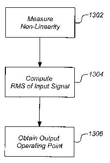
[01141 While FIG. 10 illustrates the use of the non-linear distortion maps,
knowledge of the non-linear distortion maps and operating point must be
determined.
FIG. 13 is a flow chart illustrating the determination of the operating point
in
accordance with one or more embodiments of the invention. At step 1302, TWTA
non-linearity (i.e., the AM-AM and AM-PM curves) is measured (e.g. on-line).
TWTA non-linearity may be measured in a variety of manners as described in
further
detail below.
[01151 Regardless of the technique used to measure TWTA non-linearity, the
root-
mean-squared (RMS) value of the input signal at the time of the non-linearity
measurement (used to measure the curves) is computed at step 1304. The input
signal
CA 02503532 2009-01-30
refers to the reconstructed clean signal before the imposition of TWTA
nonlinearity.
The RMS value identifies the input operating point on the measured
nonlinearity
curves.
[01161 The output operating point is then obtained at step 1306 (e. g., as a
byproduct
of the non-linearity measurement data). The output operating point may be
obtained
using a variety of methods. For example, the output operating point may be
calculated
from the RMS value of the output (received) values used to determine the TWTA
non-linearity curve (e.g., when matching the curve as described below) less
the
estimated noise power value. The output operating point may also be obtained
from
the corresponding point on the measured TWTA non-linearity curves. With the
input
and output operating points obtained, the upper layer signal (of a layered
modulation)
may be more accurately reconstructed as part of the layered modulation scheme.
[0117] It should be noted that the measurement of non-linearity (i.e., step
1302) may
be conducted in a variety of manners as part of the layered modulation scheme.
Nonetheless, regardless of the technique used to measure non-linearity, the
operating
point is estimated along with the measurement for the non-linearity curves.
The
TWTA non-linearity may be measured at the local IRDs 500, in which case the
operating point may be automatically calculated from the nonlinearity
measurements.
The TWTA non-linearity may also be made at a broadcast/uplink center 104 with
the
operating point similarly obtained, in which case information on TWTA non-
linearity
and operating point can be downloaded to individual IRDs 500, such as through
the
downlink signal 118, to support the layered modulation signal receiving
process.
6. Measuring Non-Linearity
[0118] As described above, the measurement of non-linearity (i.e., step 1302)
may be
conducted in a variety of manners as part of the layered modulation scheme. A
first
mechanism for TWTA non-linearity measurement is fully described in United
States
Patent Application Publication No. 2002/0158619, entitled "SATELLITE TWTA ON
31
CA 02503532 2009-01-30
LINE NON-LINEARITY MEASUREMENT", filed on June 7, 2002 by Ernest C.
Chen. A second measurement mechanism is fully described in United States
Provisional Patent Application Serial No. 60/510,368 (available online via
USPTO's
Public PAIR), entitled "IMPROVING TWTA AM-AM AND AM-PM
MEASUREMENT", filed on October 10, 2003, by Ernest C. Chen. The second
mechanism represents an improvement over the first mechanism. Non-linearity
may
be measured in each local IRD 500 (e. g., using a coherent averaging technique
that
maximizes signal processing gains). Non-linearity may be measured in each
local
IRD 500 (e.g., using a coherent averaging technique that maximizes signal
processing
gains).
[01191 TWTA non-linearity may be measured locally within individual IRDs. This
may, eliminate the need to transmit the non-linearity curves from the
broadcast/uplink
center 104. TWTA non-linearity can also be measured at the broadcast/uplink
center
104 using a similar estimation procedure as that described above but possibly
with a
larger receive antenna for increased CNR as desired. The IRD 802 which
receives the
downlink signal 118 (e.g., from the LNB 502) may also include a signal
processor
which extracts the symbol stream and carrier frequency from the incoming
signal and
generates an ideal signal, i.e. a signal without the effects of the TWTA and
noise. The
ideal signal is then used in a comparison processor to produce TWTA
characteristic
maps (which provide the measurements for TWTA non-linearity). As described
herein, the signal processor and comparison processor may be incorporated in
IRD
802 within the tuner/demodulator 904, FEC 506. The details concerning the
generation of the characteristic maps will be described below in the
discussion of
FIGs. 14A-14C.
[01201 Typically, the TWTA characteristic maps comprise measurements of the
output amplitude modulation versus the input amplitude modulation (the AM-AM
map) and the output phase modulation versus the input amplitude modulation
(the
AM-PM map). The received signal represents the TWTA amplifier output (plus
noise) and the generated ideal signal represents the amplifier input. In
addition to
diagnosing and monitoring the amplifier, these characteristic maps may then be
used
32
CA 02503532 2005-04-22
WO 2004/040406 PCT/US2003/033130
to facilitate and/or improve reception of lower layer signals of a system
using a
layered modulation transmission scheme.
[0121] FIGS. 14A and 14B are block diagrams of the basic system 1400 for
measuring the characteristic maps. All of the described functions may be
carried out
within a receiver 802 used in a direct broadcast satellite system having a
basic
architecture as described above. The appropriate signal section is captured
and
demodulated by demodulator 1402 which aligns symbol timing and removes any
residual carrier frequency and phase in the signal. The demodulated signal is
used in a
signal generator 1404 to generate an ideal signal, i.e. one representing the
pre-
transmitted signal. In the case of a digital signal, the signal will be
further decoded to
obtain the signal symbols which will be used to generate the ideal signal. The
difference between the ideal signal and the received signal is used by
processors 1406,
1410, 1408, 1412 to estimate a transmission non-linearity characteristic. Only
a small
section of the received signal, on the order of a few thousand symbols, may be
needed
to obtain an estimate.
[0122] FIG. 14A depicts an embodiment where the non-linearity characteristic
is
estimated from a difference between the generated ideal signal (noise-free and
without
TWTA non-linearity) and the received signal after demodulation. Because the
ideal
signal is generated from only the symbols and symbol timing, obtaining the
estimate
from the received signal after demodulation simplifies the processing.
[0123] FIG. 14B depicts an embodiment where the performance characteristic is
estimated from a difference between the ideal signal and the received signal
before
demodulation. In this case, the ideal signal must also be generated with the
carrier
frequency of the received signal. This may be done by adding the demodulated
symbol timing and carrier frequency and phase to the ideal signal.
[0124] If necessary, forward error correction (FEC) maybe applied to the
demodulated signal as part of decoding to ensure that all recovered symbols
are error-
free.
33
CA 02503532 2005-04-22
WO 2004/040406 PCT/US2003/033130
[0125] In either embodiment (FIG. 14A or 14B) the ideal signal and the
received
signal are next used in processors 1406, 1408 to pair and sort data points of
the two
signals in a two-dimensional scattergram (a scattergram for purposes herein is
the
collection of paired points with input and output values represented along X
and Y
axes, respectively). These processors 1406, 1408 characterize a relationship
between
an input signal and an output signal of the amplifier plus noise. In this
case, the input
signal is represented by the generated ideal signal 1420 (re-modulated or
otherwise)
and the output signal is represented by the received signal. The X-axis of an
AM-AM
scattergram plots the magnitudes of the ideal signal samples with perfect TWTA
linearity, and the Y-axis consists of the magnitudes of the received signal
samples
including the TWTA non-linearity (and noise). An AM-PM scattergram is
similarly
formed. The X-axis is the same as that for the AM-AM scattergram, and the Y-
axis
consists of all phase differences between the corresponding samples with and
without
TWTA non-linearity. Finally, the data points of the ideal signal and the
corresponding data points of the received signal are processed by a processor
1410,
1412 to form a line through curve fitting, such as with a polynomial. The
curve fitting
processor 1410, 1412 maybe separate or part of the processor 1406, 1408 which
paired and sorted the data points. The result is an estimate of the desired
performance
characteristic of the TWTA 1414, 1416.
[0126] FIG. 14C outlines the flow of a method of the present invention. A
signal is
received at block 1422. The signal is demodulated at block 1424. Then an ideal
signal is generated from the demodulated signal at block 1426. Finally, a
performance
characteristic (i.e., a TWTA non-linearity curve) is estimated from a
difference
between the ideal signal and the received signal at block 1428.
7. Offsetting (shifting) the TWTA Non-linearity Measurements
[0127] Independent of the operating point estimation described above, the
measured
AM-AM and AM-PM curves may be deliberately offset or shifted to simplify the
34
CA 02503532 2009-01-30
reconstruction of the upper layer signal during the signal reconstruction and
cancellation process. Such an offset does not alter the performance of layered
modulation processing (or non-linearity compensation performance). In fact,
offsetting the operating point may result in a simple and consistent
representation of
TWTA non-linearity regardless of input saturation, input backoff, etc.
[01281 To offset the measurement curves, the input and output amplitude values
(i.e., used during the non-linearity curve measurement) may be rescaled so
that the
operating point is at a desired reference point (e.g., 0 dB), for both input
and output
(e.g., thereby providing referenced operating point values). In the log
domain, such
rescaling may be performed by subtracting the measured (AM) input operating
point
value (in dB) from all input values (in dB). Likewise, the measured output
(AM)
operating point value (in dB) may be subtracted from values of all output
points (in
dB). Thus, by offsetting the measurement curves, the curves may be more easily
referenced. hi silicon and other hardware implementations, however, it may be
desirable to scale the input and output operating points or signals back (e.
g. , to-3 dB
or-5 dB) to avoid signal saturation or fractional value representation
overflow for
incoming and outgoing signals. The shifting process can be done similarly to
that
described above.
[0129] With a shifted AM scale as desired, the output PM value may also be
rescaled by subtracting the measured (angular) phase value at the output
operating
point from the phase value of all output points.
[01301 The results of the above scaling is that the operating point will
provide
reference values, such as (0 dB, 0 dB) for the AM-AM map, and (OdB, 0 ) for
the
AM-PM map. In this case the input signal must be scaled to 0 dB to match the
operating point. To guard against signal saturation errors (and to avoid the
need for a
look-up-table [LUT] extrapolation), bounding points may be placed beyond the
measured signal interval to allow interpolation of the input data (or output
testing
data) in the testing process that falls outside of the range of a TWTA
measurement
CA 02503532 2005-04-22
WO 2004/040406 PCT/US2003/033130
table. The values for the bounding points may be obtained by extrapolating or
replicating values from the endpoints of the TWTA measurement table
8. Signal Reconstruction with Complex Number Multiplications
[0131] Signal reconstruction with TWTA non-linearity, as described above,
maybe
efficiently achieved with complex number multiplications. FIG. 15A illustrates
an
intuitive algorithm for obtaining the output in-phase and quadrature
components (Io,
Qo) (that may be accomplished with separate amplitude 1502 and phase 1504
corrections as indicated) from the input in-phase and quadrature components
(I;, Q;).
In FIG. 15A, the TWTA non-linearity effect is emulated with a multiplication
on input
data. As illustrated, the input in-phase and quadrature components are
processed
through computationally-intensive rectangular-to-polar transformations 1506
(and the
inverse 1508). The non-linearity is first represented by two tables 1502 and
1504:
Table 1502 = AM-AM : M; = Mo;
Table 1504 = AM-PM : M; AO, such that
M1 exp(j91) Mo exp(j (91 + AO))
Thus, the amplitude lookup table 1502 is used to produce an output magnitude
Mo.
The above equation may be equated with the desired output expression:
M,, exp(j(91 + A9)) = M1 exp(j91)M,v exp(j9N,) (where Mw exp(j9,,) is
the multiplier for distortion) where
M,,, = M and 8,,, = AO.
M1
(Likewise, pre-distortion would be achieved by exp(j9,,,)/M,,,). Accordingly,
the
phase lookup table 1504 is used to produce the change in output phase AO. The
change in output phase AO is then added to the input phase O; to produce the
output
phase Oo. The output magnitude Mo and output phase Oo are then processed
through a
polar-to-rectangular transformation 1508 to produce the output in-phase and
quadrature components (Io, Qo).
36
CA 02503532 2005-04-22
WO 2004/040406 PCT/US2003/033130
[0132] FIG. 15 B illustrates a computationally efficient algorithm for
obtaining the
input and output operating points (Io, Qo). In FIG. 15B, the LUTs (in (M, 0))
1502
and 1504 (in FIG. 15A) are replaced with one complex multiplier LUT 1510 in
(I,Q).
The entries of the LUT is calculated from:
1. + jQw = M" exp(j,& 9w)
The efficient algorithm begins with at 1512 with a computation of the signal
power.
The signal power computation 1512 is followed by a table lookup 1510 using the
input signal power to index the proper complex multiplier (IW, QW). The
complex
multiplier (IW, Qw) is then multiplied with the incoming complex-valued data
to effect
the TWTA distortion distortion:
Io +jQO =(II +jQ,)(IW+jQQ)
[0133] Accordingly, the efficient scheme of FIG. 15B avoids computationally
intensive rectangular-to-polar and inverse transformations 1506 and 1508 and
requires
simple power formation 1512 and a complex number multiplication through an LUT
1510. In addition, the efficient scheme may include a complex matching factor
in the
complex multiplier table 1510, the matching factor being the magnitude and
phase
difference between the upper and lower layer components of a layered
modulation
signal if desired.
Conclusion
[0134] This concludes the description of the preferred embodiments of the
present
invention. The foregoing description of the preferred embodiment of the
invention
has been presented for the purposes of illustration and description. It is not
intended
to be exhaustive or to limit the invention to the precise form disclosed. Many
modifications and variations are possible in light of the above teaching. For
example,
it is noted that the uplink configurations depicted and described in the
foregoing
disclosure can be implemented by one or more hardware modules, one or more
37
CA 02503532 2005-04-22
WO 2004/040406 PCT/US2003/033130
software modules defining instructions performed by a processor, or a
combination of
both.
[0135] It is intended that the scope of the invention be limited not by this
detailed
description, but rather by the claims appended hereto. The above
specification,
examples and data provide a complete description of the manufacture and use of
the
apparatus and method of the invention. Since many embodiments of the invention
can
be made without departing from the scope of the invention, the invention
resides in
the claims hereinafter appended.
38