Note: Descriptions are shown in the official language in which they were submitted.
CA 02503817 2005-04-26
WO 2004/042430 PCT/US2003/034607
1
WAVELENGTH INSENSITIVE INTEGRATED
OPTIC POLARIZATION SPLITTER
PRIORITY INFORMATION
This application claims priority from provisional application Ser. Nos.
60/422,413 filed October 30, 2002, and 60/478,767 filed June 16, 2003,
incorporated herein by reference in their entirety.
BACKGROUND OF THE INVENTION
The invention relates to the field of integrated optic polarization splitters,
and in particular to an integrated optic polarization splitter based on the
intersection or near intersection of horizontally and vertically oriented
waveguides.
As the prevalence of fiber optic communication grows, the demand for
more intricate processing of optical signals continues to increase. Since
integrated optic devices allow for integration of many optical functions on a
chip,
integrated optic approaches will likely fill the demand for more intricate
optical
signal processing. However, in order to improve the functionality and reduce
the
cost per function the density of components on the chip must increase.
For a given wavelength, the confinement of a mode in a dielectric
waveguide is determined by the contrast between the core and cladding indices,
the higher the contrast, the tighter the confinement. An outgrowth of tighter
confinement is the ability to pack waveguides closer together and guide light
around sharper bends without substantial radiative loss. Since these are the
two
most critical parameters affecting device density, it can generally be said
that the
higher the index contrast the greater the device density. However, as the
index
contrast increases, the transverse electric (TE) and transverse magnetic (TM)
modes propagating in the waveguides begin to exhibit different
characteristics.
While in a straight section of a square waveguide, the TE and TM modes
propagate at the same rate, in a bend the TE and TM modes propagate at
substantially different rates. And, when a pair of square high index contrast
(HIC) guides is coupled, the TE and TM modes tend to couple at different
rates.
CA 02503817 2005-04-26
WO 2004/042430 PCT/US2003/034607
2
Since most integrated optic components are sensitive to both propagation
velocity
and guide-to-guide coupling, these effects result in polarization dependent
performance, a result that is not compatible with the random polarization
state
emanating from the standard single mode fiber used in telecom applications.
One way to compensate these effects is to use a rectangular waveguide
geometry and alter the aspect ratio of the guide to compensate for the natural
difference in propagation around a bend and/or equalize the guide-to-guide
coupling. However, while one or the other of these effects may be compensated
in this manner for a particular device, as the index contrast increases it
becomes
difficult if not impossible to compensate both simultaneously in a manner that
applies to all devices on the chip.
Another approach for overcoming the polarization sensitivity of HIC
integrated optics is to split the random input polarization emanating from the
single mode (SM) fiber with a polarizing beam splitter (PBS), couple the
outputs
to polarization maintaining (PM) fibers, twist one of these PM fibers by
90°
degrees and couple the two fibers to separate paths on the integrated optic
chip.
On each of these paths identical structures are used to process the two
components independently. At the output, these components are recombined by
coupling to another pair of PM fibers, twisting the PM fiber of the path that
had
not previously been twisted and coupling both fibers to another PBS which has
a
SM fiber output. While such an approach, commonly referred to as a
"polarization diversity" scheme, is feasible, when implemented with bulk
optics
it is also cumbersome. Aligning PM fibers is difficult and expensive. And, in
order to preserve signal integrity the path lengths must be matched to within
at
least one-tenth of a bit length (i.e. ~mm for lOGb/s signals and -O.Smm for
40Gbls signals assuming an index of 1.5).
A better approach is to integrate the splitting function of the PBS and the
rotating function of the twisted PM fiber onto the integrated optic chip.
Doing so
would eliminate the need to align PM fibers and path lengths could be matched
easily through lithography.
Several integrated optic polarization splitters and rotators (or converters)
have been proposed. However, most of the devices proposed to date rely on the
CA 02503817 2005-04-26
WO 2004/042430 PCT/US2003/034607
3
coupling of a pair of waveguide modes. Devices based on coupled modes
generally exhibit a wavelength sensitivity resulting from differences in the
dispersion of the super-modes propagating in the structure. Further, such
approaches are very sensitive to fabrication errors. Even slight changes in
the .
waveguide geometries or separation can have a significant impact on the device
performance.
A better way to form a polarization splitter or rotator is to use the
principle of mode evolution. By making gradual (or adiabatic) changes to the
waveguide geometry, the modes in the guide can be conditioned and the
polarization states separated or rotated. Such an approach only requires that
the
modes not exchange power which can be assured by proper design of the
waveguide and a slow evolution of the structure. Since prevention of mode
coupling is a relatively loose requirement, devices based on mode evolution
tend
to be wavelength insensitive and fabrication tolerant. It has been proposed
and
demonstrated that a polarization splitter based on mode evolution can be
formed,
however, this approach has the disadvantage of requiring multiple waveguide
materials .
Generally, it is the object of the present invention to split polarization
states with an integrated optic device based on the principle of mode
evolution.
It is a further object of the present invention that when run in reverse the
device operate as a polarization combiner.
It is yet another object of the present invention that the device be
wavelength insensitive, tolerant to fabrication errors, and require only a
single
material system to construct.
These and other objects of the present invention will become apparent to
those skilled in the art from the following detailed description and
accompanying
figures.
SUMMARY OF THE INVENTION
According to one aspect of the invention, there is provided an integrated
optic polarization splitter. The polarization splitter includes an input
waveguide
element that inputs an optical signal having TE and TM components. A
CA 02503817 2005-04-26
WO 2004/042430 PCT/US2003/034607
' 4
vertically oriented waveguide element which includes a plurality of core
layers is
coupled to the input waveguide element and propagates the TM component of the
optical signal. A horizontally oriented waveguide element is coupled to the
input
waveguide element and propagates the TE component of the optical signal.
According to another aspect of the invention, there is provided a method
of forming an integrated optic polarization sputter. The method includes
providing an input waveguide element that inputs an optical signal having TE
and
TM components. Moreover, the method includes forming a vertically oriented
waveguide element that is coupled to the input waveguide element and
propagates
the TM component of the optical signal. The vertically oriented waveguide
element includes a plurality of core layers. Furthermore, the method includes
forming a horizontally oriented waveguide element that is coupled to the input
waveguide element that propagates the TE component of the optical signal.
According to another aspect of the invention, there is provided an
integrated optic polarization splitter. The integrated optic polarization
splitter
includes a pair of waveguide elements with a first waveguide element having a
horizontal orientation and a second waveguide element having a vertical
orientation formed from a plurality of waveguide core layers. The first and
second waveguide elements are intersected or nearly intersected at one end of
the
structure and separated at the other end of the structure so that the
transition is
made to be adiabatic. The waveguide elements receive an optical signal having
both a TE component and a TM component. The TE component propagates
along the horizontally oriented waveguide element and the TM component
propagates along the vertically oriented waveguide element.
BRIEF DESCRIPTION OF THE DRAWINGS
FIG. 1 is a schematic diagram of a polarization splitter in accordance with
the invention;
FIGs. 2A-2B are schematic diagrams of mode scattering calculations of
the TE and TM fields propagating in the polarization splitter depicted in FIG.
l;
and
FIGS. 3A-3B are graphs demonstrating the performance of the
CA 02503817 2005-04-26
WO 2004/042430 PCT/US2003/034607
polarization splitter depicted in FIG 1; and
FIGS. 4A-4C are schematic diagrams of polarization splitters utilizing
three core layers with a gap between the middle core layers of the vertically
and
horizontally oriented waveguide elements; and
5 FIG. 5 is a schematic diagram of a polarization splitter utilizing only two
core layers with a gap between the middle core layers of the vertically and
horizontally oriented waveguide elements; and
FIGs. 6A-6B are graphs demonstrating the performance of the
polarization splitter depicted in FIG 5; and
FIGS. 7A-7B are schematic diagrams of polarization splitters utilizing two
core layers with alternate transition regions into the structure.
DETAILED DESCRIPTION OF THE INVENTION
The polarization splitter of the invention is constructed from the
intersection or near intersection of a pair of waveguides. The zone in which
the
waveguides are in closest proximity is the splitter input and the zone in
which they
are at their greatest separation is the splitter output. For the device to
efficiently
separate the polarization states, the fundamental TE (or quasi TE) mode of the
combined structure at the device input must evolve into the fundamental mode
of
one of the guides, denoted the TE guide, while the fundamental TM (or quasi
TM)
mode evolves into the fundamental mode of the other guide, denoted the TM
guide. For this to occur, the TM mode of the TM guide must be more strongly
guided (have a higher effective index) than the TM mode of the TE guide.
Similarly, the TE mode of the TE guide must be more strongly guided than the
TE
mode of the TM guide.
The evolution of the waveguide acts as a perturbation to the mode
structure inducing coupling amongst the modes in the system, the faster the
evolution, the stronger the coupling. In order to ensure that the structure
acts as
a polarization splitter, coupling amongst the fundamental modes and between
the
fundamental modes and other modes in the system must be inhibited. The full
spectrum of modes in the structure consists of the fundamental guided TE and
TM modes, unguided (or radiation) modes, and secondary guided TE and TM
modes that appear as the horizontally and vertically oriented sections
separate.
CA 02503817 2005-04-26
WO 2004/042430 PCT/US2003/034607
6
The unguided modes propagate at substantially faster rates than the
fundamental
modes. As a result, when the transition is sufficiently weak, the modes have a
chance to de-phase before substantial power exchange occurs. Therefore, power
exchange between fundamental modes and radiation modes can be substantially
reduced by making the transition slow (or adiabatic). Coupling between
fundamental modes and secondary guided modes can be similarly inhibited by
ensuring that the secondary modes also propagate at substantially higher
rates.
This can be done by forming the structure from a pair of guides with principal
axes
that are orthogonally oriented. In the electromagnetic sense, the principal
axis is
defined by the electric field polarization of the fundamental mode of the
waveguide. For a rectangular buried waveguide, the principal axis is along the
larger of the two dimensions that define the rectangle. In the present
description,
when specifying an orientation of a waveguide, reference is made to the
principal
axis of the waveguide. For example, the expression "vertically oriented
waveguide
section" is meant to indicate a waveguide section having a principal axis that
is
vertical, i.e., orthogonal to a main planar surface (such as the substrate
surface) of
the waveguide device, while the expression "horizontally oriented waveguide
section" is meant to indicate a waveguide section having a principal axis that
is
horizontal, i.e., parallel to a main planar surface (such as the substrate
surface) of
the waveguide device.
Finally, coupling amongst the fundamental modes can be inhibited by
further ensuring that the fundamental modes propagate at different rates
and/or
by positioning the guides in such a manner to prevent coupling through mode
symmetry.
As a final generality it is important to note that a device which acts as an
effective polarization splitter, will through the principle of reciprocity,
act as an
effective polarization combiner when run in reverse.
Practical implementations of the device typically require that it be formed
from micro-fabrication techniques, which generally require the structures be
formed from a layering process with features defined through lithography. It
is
therefore desirable to build the structure with as few layers as possible.
Herein,
a layer is defined as a horizontal slice through the waveguide cross-section
which
contains no variations of refractive index in the vertical direction.
CA 02503817 2005-04-26
WO 2004/042430 PCT/US2003/034607
7
The optical waveguides forming the inventive polarization splitter are
typically formed by dielectric materials of various refractive indices.
Generally,
the higher index materials are considered core materials while the lower index
materials are considered cladding materials. To be specific, a cladding
material
is herein defined as the material of lowest refractive index within a layer.
All
other materials within the layer are therefore core materials. A core layer is
defined as a layer containing a core material.
The basic requirements for the structure to operate as a polarization
splitter are quite loose, with the primary requirement being that the
structure be
formed from the intersection or near intersection of a pair of orthogonally
oriented waveguides which separate thereby splitting the orthogonally oriented
modes into the respective orthogonally oriented waveguide sections. A few of
the possible geometries are described below.
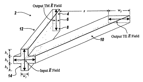
FIG. 1 is a schematic diagram of a polarization splitter 2 in accordance
with the invention. The splitter 2 begins as a pair of orthogonally oriented
rectangular waveguides 14 which are centrally intersected and then gradually
separated into a pair of rectangular waveguides 10, 12, one with a horizontal
orientation 10, and the other with a vertical orientation 12, with a final
separation
of s as shown in FIG. 1. A cladding, with a lower refractive index than the
core
layers typically surrounds the core layers to provide light confinement. The
polarization splitter in FIG. 1 uses centrally intersected waveguides to
inhibit
coupling amongst the fundamental guided modes. As a result, the structure will
typically require a minimum of three core layers 4, 6, and 8 with heights hl,
h2,
and h3 where 7~1 and h3 are preferably designed to be equal. The horizontally
oriented waveguide 10 has a width w2 and height h3, and the vertically
oriented
waveguide 12 has a width w1 and height that is the sum of h,, ha, and h3. At
the
input of the polarization splitter only two guided modes exist, a fundamental
TE
mode and a fundamental TM mode. At large separations of the horizontally
oriented and vertically oriented sections, the fundamental TE mode is almost
entirely confined to the horizontally oriented section and the fundamental TM
mode is confined to the vertically oriented section. Thus, the natural
evolution of
the fundamental modes results in a splitting of the TE and TM components.
CA 02503817 2005-04-26
WO 2004/042430 PCT/US2003/034607
It is important to note that many variations of the described embodiment
are possible. The waveguides need not be rectangular in geometry and the core
layers need not have the same refractive indices or geometry.
FIGS. 2A-2B are schematic diagrams of mode-scattering simulations of
TE and TM fields propagating in the polarization splitter of FIG 1. The mode
scattering technique takes overlaps between the local modes at each cross-
section
along the length of the structure and propagates the field between cross-
sections.
Since a reduced set of modes are typically used to minimize the calculation
time,
mode scattering simulations are a particularly useful modeling tool only when
a
few modes per waveguide cross-section are required to represent the system.
Since the radiation modes do not substantially influence the operation of
approaches based on mode evolution, the mode-scattering technique is well
suited
for these problems. In the embodiment used for these simulations, the core
refractive index is 2.2 and the cladding index is 1.445. The dimensions of the
horizontally and vertically oriented waveguide cores are 0.25 x 0.75 ~,m and
0.75
x 0.25 Vim, respectively, indicating a layer thickness of 0.25 ~,m. The length
of
the splitter is 30 ~,m and the distance separating the horizontally oriented
rectangular waveguide 22 and vertically oriented rectangular waveguide 20 is 1
~,m at the device output. However, other dimensions can be used in other
embodiments.
FIG. 2A shows the TE field propagating in the splitter 2. In particular,
the TE field propagates in the horizontally oriented rectangular waveguide 22
and
not the vertically oriented rectangular waveguide 20.
FIG. 2B shows the TM field propagating in the splitter. The TM field
propagates in the vertically oriented rectangular waveguide 20 and not the
horizontally oriented rectangular waveguide 22. Thus, FIGs. 2A-2B demonstrate
the ability of the sputter to separate TE and TM components of a randomly
polarized input signal.
FIGs. 3A-3B are graphs of mode-scattering and full three dimensional
finite difference time domain (FDTD) simulations, respectively, demonstrating
the performance of the polarization splitter depicted in FIG 1. Here again,
the
core refractive index is 2.2 and the cladding index is 1.445. The dimensions
of
CA 02503817 2005-04-26
WO 2004/042430 PCT/US2003/034607
9
the waveguide cores are 0.25 x 0.75 ~,m and 0.75 x 0.25 ,um, respectively,
indicating a layer thickness of 0.25 ~,m. The waveguide elements are separated
at the output by a distance s = 1 ~,m. FIG. 3A shows the relationship between
the length of the inventive polarization splitter and the normalized output
modal
power for the TE and TM modes. In particular, FIG. 3A shows that for lengths
that are larger than 25 ~.m, the normalized output modal power for both the
TEl
(fundamental TE) mode and TMiI (fundamental TM) modes are nearly 1 with
very little cross-talk (TEII to TEz, and TMI1 to TM21 coupling) over the
entire
1.45 ~,m to 1.65 ~,m band. The performance of the inventive splitter improves
as
the transition becomes more adiabatic.
FIG. 3B demonstrates the wavelength insensitive nature of the device
from 1.45 ~,m to 1.65 ,um) which includes the telecom wavelengths using a full
three-dimensional FDTD simulation. The FDTD method is a numerical
implementation of Maxwell's equations with the only errors being those caused
by the grid discretization. In contrast to the mode-scattering technique all
modes
of the system are taken into account. For the present simulation the device
length is 25 ~.m. In this range, the normalized output modal power for both
the
TEI, mode and TMII modes are nearly 1 with very little cross-talk (TEII to
TE2,
and TMII to TM21 coupling) over the entire 1.45 ~,m to 1.65 ~,m band. This
indicates that the inventive splitter device does not possess any significant
wavelength sensitivity in the telecom wavelength regime.
FIGS. 4A-4C are diagrams of polarization sputters 100, 102, and 104 in
which the vertically 106, 108, and 110 and horizontally oriented waveguides
112,
114, and 116 do not have a point of intersection. Although in theory the
performance of the device depicted in FIG. 1 is nearly ideal, when fabricated
some rounding may occur in the region where the two waveguides intersect.
This rounding will only occur in the middle layers 118, 120, and 122 and is a
result of the limited resolution of optical lithography.
However, the impact on performance may be substantial as this would
lead to a rather abrupt junction in the waveguides 10 and 12 of FIG. 1. Hence,
it
would be desirable to remove the intersection point. This can be accomplished
by keeping the middle layers 118, 120, 122 of the vertically oriented
waveguides
CA 02503817 2005-04-26
WO 2004/042430 PCT/US2003/034607
106, 108, and 110 separated from the horizontally oriented waveguides 112,
114,
and 116 by a small gap sl. So long as the gap s, is greater than the
resolution
limit of the lithographic system, the fabrication error will be removed. Note
that
the dimensions of the vertically oriented waveguide 106, 108, and 110 and
5 horizontally oriented waveguide 112, 114, and 116 are similar to those
described
for vertically oriented waveguide 12 and horizontally oriented waveguide 10 in
FIG. 1. Note that the vertically oriented 106, 108, and 110 and horizontally
oriented waveguides 112, 114, and 116 are separated by a distance s2.
FIGs. 4A-4C demonstrate a few of the many ways in which to transition
10 into the inventive polarization splitter with a gap between the guides in
the
middle layers 118, 120, and 122. In particular, FIG. 4A tapers the vertically
oriented waveguide 106 to transition the input modes into the polarization
splitter
adiabatically. In FIG. 4B the various pieces of the core in the layers 130,
120,
134 forming the vertically oriented waveguide 108 are separately and
adiabatically brought into proximity with the horizontally oriented waveguide
114
so as to ensure that both the fundamental TE and TM modes originate in the
horizontally oriented waveguide 114. Finally, in FIG. 4C, a reduced width
vertically oriented waveguide 110 is brought into proximity with the
horizontally
oriented waveguide 116 and subsequently tapered into the full width structure
again assuring that the fundamental modes originate in the input horizontally
oriented waveguide 116.
All of these approaches work on the same principle. The modes of the
input waveguide must be adiabatically transitioned in the inventive
polarization
splitter wherein the orthogonally oriented waveguides are in close proximity.
The approach taken will typically depend on the fabrication technology
utilized.
These geometries represent just a few of the many possible ways of coupling to
the inventive polarization splitter. The waveguide sections need not be
rectangular in geometry and the core layers need not have the same refractive
indices or geometry.
FIG. 5 shows a polarization splitter 54 which requires only two core
layers 60, 62 to fabricate. In this embodiment, the vertically oriented 58 and
horizontally oriented 56 waveguides are no longer centrally intersected. As a
result, the fundamental TE and TM modes couple to one another. However, this
CA 02503817 2005-04-26
WO 2004/042430 PCT/US2003/034607
11
coupling may again be mitigated by ensuring the fundamental modes propagate at
different rates and have a chance to de-phase before substantial power
exchange
occurs. This is accomplished by making the horizontally oriented 56 and
vertically oriented 58 waveguides different sizes. The performance of the
device
is unaffected by the ordering of the layers (i.e. which layer sits on top).
Note
that the two core layers 60, 62 have heights hl, h2. The structure also leaves
a
gap s~ between the orthogonally oriented waveguides at the input to facilitate
fabrication. At the output the vertically oriented waveguide 58 and
horizontally
oriented waveguide 56 are separated by a distance sa. In addition, the
horizontal
waveguide 56 has a width w~ and height h~, and the vertical waveguide 12 has a
width w, and height that is the sum of hl and ha.
It is important to note that many variations of the described embodiment
are possible. The waveguide sections need not be rectangular in geometry and
the core layers need not have the same refractive indices or geometry.
FIGS. 6A-6B are graphs of mode-scattering and FDTD simulations,
respectively, of the performance of the device depicted in FIG. 5. In this
particular embodiment, the core refractive index is 2.2 and the cladding index
is
1.445. The layer thicknesses are each 0.4 ~.m and the guide widths are 0.35
,um
and 0.8 ~,m for the vertically and horizontally oriented waveguides,
respectively.
The input and output separations of the guides are chosen to be s, = 0.25 ~,m
and
s2 = 1.0 ~,m, respectively.
In particular FIG. 6A shows the performance of the device depicted in
FIG. 5 as a function of the device length at a wavelength of 1.55 ,um. The
graph
shows that for lengths over 150 pm, the performance of this two layered
polarization splitter is nearly ideal. FIG. 6B demonstrates the performance of
the
device depicted in FIG. 5 as a function of wavelength for a device length of
143
wm. FIG. 6B shows that the device is largely wavelength insensitive with very
little cross-talk (TEl1 to TE21 and TMI, to TM2, coupling) over the entire
1.45 ~,m
to 1.65 ,um regime.
FIGS. 7A-7B demonstrate a couple of the many ways in which to
transition into the inventive two layer polarization splitter with a gap s,
between
the guides in the middle layers 82, 84. The approaches are analogous to those
taken in a three layer device. In FIG. 7A, a reduced width vertically oriented
CA 02503817 2005-04-26
WO 2004/042430 PCT/US2003/034607
12
waveguide 68 is brought into proximity with the horizontally oriented
waveguide
66 and subsequently tapered into the full width structure. In FIG. 7B the
various
layers 72, 74 forming the vertically oriented waveguide 76 are separately and
adiabatically brought into proximity with the horizontally oriented waveguide
80.
Again, each of these approaches has advantages and disadvantages with respect
to
fabrication, but all work on the same principle. The modes of the input
waveguide must be adiabatically transitioned into the inventive polarization
splitter by gradually bringing the orthogonally oriented waveguides into close
proximity. The approach taken will typically depend on the fabrication
technology utilized. These geometries represent just a few of the many
possible
ways of coupling to the inventive polarization splitter. The waveguide
sections
need not be rectangular in geometry and the core layers need not have the same
refractive indices or geometry.
Importantly, the principle of reciprocity ensures that all of the
aforementioned embodiments will act as polarization combiners when run in
reverse.
Although the present invention has been shown and described with respect
to several preferred embodiments thereof, various changes, omissions and
additions to the form and detail thereof, may be made therein, without
departing
from the spirit and scope of the invention.
What is claimed is: