Note: Descriptions are shown in the official language in which they were submitted.
CA 02503854 2005-04-26
WO 2004/059706 PCT/US2003/040483
METHODS OF FORMING ELECTRONIC DEVICES
INCLUDING SEMICONDCUTOR MESA STRUCTURES AND
CONDUCTIVITY JITNCTIONS AND RELATED DEVICES
Related Applications
The present application claims the benefit of; U.S. Provisional Application
No. 60/435,213 filed December 20, 2002, and entitled "Laser Diode With Self
Aligned
Index Guide And Via"; U.S. Provisional Application No. 60/434,914 filed
December-
s 20, 2002, and entitled "Laser Diode With Surface Depressed Ridge Waveguide";
U.S.
Provisional Application No. 60/434,999 filed December 20, 2002 and entitled
"Laser
Diode with Etched Mesa Structure"; and U.S. Provisional Application No.
60/435,211
filed December 20, 2002, and entitled "Laser Diode With Metal Current
Spreading
Layer." The disclosures of each of these provisional applications are hereby
incorporated herein in their entirety by reference.
The present application is also related to: U.S. Application No. .
(Attorney Docket No. 5308-281) entitled "Methods Of ,Forming Semiconductor
Devices Having SelfAligned Semiconductor Mesas and Contact Layers And Related
Devices" filed concurrently herewith; U.S. Application No. (Attorney
Docket No. 5308-282) entitled "Methods Of Forming Semiconductor Devices
Including Mesa Structures And Multiple Passivation Layers And Related Devices"
filed concurrently herewith; and U.S. Application No. (Attorney Docket
No. 5308-280) entitled "Methods Of Forming Semiconductor Mesa Structures
Including Self Aligned Contact Layers And Related Devices" filed concurrently
herewith. The disclosures of each of these U.S. Applications are hereby
incorporated
herein in their entirety by reference.
Field Of The Invention
The. present invention relates to the field of electronics, and more
particularly,
to methods of forming electronic semiconductor devices and related structures.
Background Of The Invention
A laser is a device that produces a beam of coherent monochromatic light as a
result of stimulated emission of photons. Stimulated emission of photons may
also
produce optical gain, which may cause light beams produced by lasers to have a
high
CA 02503854 2005-04-26
WO 2004/059706 PCT/US2003/040483
optical energy. A number of materials are capable of producing the lasing
effect and
include certain high-purity crystals (ruby is a common example),
semiconductors,
certain types of glass, certain gases including carbon dioxide, helium, argon
and neon,
and certain plasmas.
More recently, lasers have been developed in semiconducting materials, thus
taking advantage of the smaller size, lower cost and other related advantages
typically
associated with semiconductor~devices. In the semiconductor arts, devices in
which
photons play a major role are referred to as "photonic" or "optoelectronic"
devices. In
turn, photonic devices include light-emitting diodes (LEDs), photodetectors,
photovoltaic devices, and semiconductor lasers.
Semiconductor lasers are similar to other lasers in that the emitted radiation
has spatial and temporal coherence. As noted above, laser radiation is highly
monochromatic (i.e., of narrow band width) and it produces highly directional
beams
of light. Semiconductor lasers may differ, however, from other lasers in
several
respects. For example, in semiconductor lasers, the quantum transitions are
associated with the band properties of materials; semiconductor lasers may be
very
compact in size, may have very narrow active regions, and;larger divergence of
the
laser beam; the characteristics of a semiconductor laser may be strongly
influenced by
the properties of the junction medium; and for P-N junction lasers, the lasing
action is
produced by passing a forward current through the diode itself. Overall,
semiconductor lasers can provide very efficient systems that may be controlled
by
modulating the current directed across the devices. Additionally, because
semiconductor lasers can.have.very short photon lifetimes, they may be used to
produce high-frequency modulation. In turn, the compact size and capability
for such
high-frequency modulation may make semiconductor lasers an important light
source
for optical fiber communications.
In broad terms, the structure of a semiconductor laser should provide optical
confinement to create a resonant cavity in which light amplification may
occur, and
electrical confinement to produce high current densities to cause stimulated
emission
to occur. Additionally, to produce the laser effect (stimulated emission of
radiation),
the semiconductor may be a direct bandgap material rather than an indirect
bandgap
material. As known to those familiar with semiconductor characteristics, a
direct
bandgap material is one in which an electron's transition from the valence
band to the
conduction band does not require a change in crystal momentum for the
electron.
CA 02503854 2005-04-26
WO 2004/059706 PCT/US2003/040483
Gallium arsenide and gallium nitride are examples of direct bandgap
semiconductors.
In indirect bandgap semiconductors, the alternative situation exists; i.e., a
change of
crystal momentum is required for an electron's transition between the valence
and
conduction bands. Silicon and silicon carbide are examples of such indirect
semiconductors.
A useful explanation of the theory, structure and operation of semiconductor
lasers, including optical and electronic confinement and mirroring, is given
by Sze,
Physics of Semiconductor Devices, 2nd Edition (1981) at pages 704-742, and
these
pages are incorporated entirely herein by reference.
As known to those familiar with photonic devices such as LEDs and lasers, the
frequency of electromagnetic radiation (i.e., the photons) that can be
produced by a
given semiconductor material may be a function of the material's bandgap.
Smaller
bandgaps produce lower energy, longer wavelength photons, while wider bandgap
materials produce higher energy, shorter wavelength photons. For example, one
semiconductor commonly used for lasers is aluminum indium gallium phosphide
(AlInGaP). Because of this material's bandgap (actually a range of bandgaps
depending upon the mole or atomic fraction of each element present), the light
that
AIInGaP can produce may be limited to the red portion of the visible spectrum,
i.e.,
about 600 to 700 nanometers (nm). In order to produce photons that have
wavelengths in the blue or ultraviolet portions of the spectrum, semiconductor
materials having relatively large bandgaps may be used. Group Ill-nitride
materials
such as gallium nitride (GaN), the ternary alloys indium gallium nitride
(InGaN),
aluminum gallium nitride (AIGaN) and aluminum indium nitride (AlInN) as well
as
the quaternary alloy aluminum gallium indium nitride (AIInGaN) are attractive
candidate materials for blue and UV lasers because of their relatively high
bandgap
(3.36 eV at room temperature for GaN). Accordingly, Group Ill-nitride based
laser
diodes have been demonstrated that emit light in the 370-420 nm range.
A number of commonly assigned patents and co-pending patent applications
likewise discuss the design and manufacture of optoelectronic devices. For
example,
U.S. PatentNos. 6,459,100; 6,373,077; 6,201,262; 6,187,606; 5,912,477; and
5,416,342' describe various methods and structures for gallium-nitride based
optoelectronic devices. U.S. Patent No. 5,838,706 describes low-strain nitride
laser
diode structures. Published U.S. Application Nos. 20020093020 and 20020022290
describe epitaxial structures for nitride-based optoelectronic devices.
Various metal
CA 02503854 2005-04-26
WO 2004/059706 PCT/US2003/040483
contact structures and bonding methods, including flip-chip bonding methods,
are
described in Published U.S. Application No. 20020123164 as well as Published
U.S.
Application No. 030045015 entitled "Flip Chip Bonding of Light Emitting
Devices
and Light Emitting Devices Suitable for Flip-Chip Bonding"; Published U.S.
Application No. 20030042507 entitled "Bonding of Light Emitting Diodes Having
Shaped Substrates and Collets for Bonding of Light Emitting Diodes Having
Shaped
Substrates", and Published U.S. Application No. 2003.O.Q15721 entitled "Light
Emitting Diodes Including Modifications for Submount Bonding and Manufacturing
Methods Therefor." Dry etching methods are described in U.S. Patent No.
6,475,889.
Passivation methods for nitride optoelectronic devices.are described in U.S.
Application Ser. No. 08/920,409 entitled "Robust Group III Light Emitting
Diode for
High Reliability in Standard Packaging Applications" and Published U.S.
Application
No. 20030025121 entitled "Robust Group III Light Emitting Diode for High
Reliability in Standard Packaging Applications." Active layer structures
suitable for
use in nitride laser diodes are described in Published U.S. Application No.
20030006418 entitled "Group III Nitride Based Light Emitting Diode Structures
with
a Quantum Well and Superlattice, Group III Nitride Based Quantum Well
Structures
and Group III Nitride Based Superlattice Structures" and Published U.S.
Application
No. 20030020061 entitled "Ultraviolet Light Emitting Diode." The contents of
all of
the foregoing patents, patent applications and published patent applications
are
incorporated entirely herein by reference as if fully set forth herein.
Not withstanding the structures and methods discussed above, further
structures and/or methods providing improved beam quality, stability, voltage
characteristics, guiding, and/or operating current characteristics may be
desired.
Summary
According to embodiments of the present invention, a light emitting device
may include a silicon carbide substrate, and a semiconductor structure on the
substrate. More particularly, the semiconductor structure may include a mesa
having
a mesa base adjacent the substrate, a mesa surface opposite the substrate, and
mesa
sidewalls between the mesa surface and the mesa base. In addition, the
semiconductor structure may have a first conductivity type adjacent the
silicon
carbide substrate, the semiconductor structure may have a second conductivity
type .
adjacent the mesa surface, and the semiconductor structure may have a junction
CA 02503854 2005-04-26
WO 2004/059706 PCT/US2003/040483
between the first and second conductivity types. Moreover, the mesa may be
configured to provide at least one of current confinement or optical
confinement for a
light emitting device in the semiconductor structure.
In one alternative, the junction may be between the mesa base and the mesa
surface. In another alternative, the semiconductor structure may include a
semiconductor base layer between the mesa base and the silicon carbide
substrate and
the junction may be between a surface of the base layer opposite the silicon
carbide
substrate and the silicon carbide substrate. Moreover, the semiconductor
structure
may include a Group III-V semiconductor material.
According to more embodiments of the present invention, an electronic device
may include a substrate and a semiconductor mesa on the substrate. More
particularly, the semiconductor mesa may have a mesa base adjacent the
substrate, a
mesa surface opposite the substrate, and mesa sidewalls between the mesa
surface and
the mesa base. Moreover, the semiconductor mesa may have a first conductivity
type
between the mesa base and a junction, the junction may be between the mesa
base and
the mesa surface, and the semiconductor mesa may have a second conductivity
type
between the junction and the mesa surface.
The junction may comprise a physical location where doping of the second
conductivity type begins, the first conductivity type may be N-type, and the
second
conductivity type.may be P-type. The semiconductor mesa may comprise a Group
III-V semiconductor material such as a Group III-nitride semiconductor
material.
In addition, the junction may be no more that approximately 5 microns from
the mesa base; and more particularly, the junction may be no more than
approximately 0.75 microns from the mesa base. Moreover, the junction may be
at
least approximately 0.05 microns from the mesa base, and more particularly,
the
junction may be at least approximately 0.1 microns from the mesa base. The
semiconductor mesa may have a thickness in the range of approximately 0.1
microns
to 5 microns.
A semiconductor base layer may be included between the substrate and the
semiconductor mesa, and the semiconductor base layer may have the first
conductivity type throughout. More particularly, the semiconductor base layer
may
have a thickness no greater than approximately 5 microns, and each of the
semiconductor base, layer and the semiconductor mesa may comprise a Group III-
V
semiconductor material. In addition, the substrate may comprise silicon
carbide.
CA 02503854 2005-04-26
WO 2004/059706 PCT/US2003/040483
According to additional embodiments of the present invention, an electronic
device may include a substrate, a semiconductor base layer on the substrate,
and a
semiconductor mesa on a surface of the base layer opposite the substrate. The
semiconductor base layer may have a first conductivity type between the
substrate and
, a junction, the junction may be between the substrate and a surface of the
base layer
opposite the substrate, and the semiconductor base layer may have a second
conductivity type between the junction and the surface of the base layer
opposite._the
substrate. The semiconductor mesa may have a mesa surface opposite the
semiconductor base layer and mesa sidewalls between the mesa surface and the
base
layer, and the semiconductor mesa may have the second conductivity type
throughout.
The junction may be a physical location where doping of the second
conductivity type begins, the first conductivity type may be N-type, and the
second
conductivity type may be P-type. Each of the semiconductor mesa and the
semiconductor base layer may comprise a Group III-V semiconductor material
such
as a Group III-nitride semiconductor material.
The junction may be no more that approximately 0.4 microns from the surface
of the base layer opposite the substrate, and more particularly, the junction
may be no
more than approximately 0.2 microns from the surface of the base layer
opposite the
substrate. In addition, the junction may be at least approximately 0.05
microns from
the surface of the base layer opposite the substrate, and more particularly,
the junction
may be at least approximately 0.1 microns from the surface of the base layer
opposite
the substrate. Moreover, the semiconductor mesa may have a thickness in the
range
of approximately 0.1 microns to 5 microns, the semiconductor base layer may
have a
thickness no greater than approximately 5 microns. In addition, the substrate
may
comprise silicon carbide
According to still additional embodiments of the present invention, methods of
forming an electronic device may include forming a semiconductor mesa on a
substrate. The semiconductor mesa may have a mesa base adjacent the substrate,
a
mesa surface opposite the substrate, and mesa sidewalls between the mesa
surface and
the mesa base. Moreover, the, semiconductor mesa may have a first conductivity
type
between the mesa base and a junction, the junction may be between the mesa
base and
the mesa surface, and the semiconductor mesa may have a second conductivity
type
between the junction and the mesa surface.
CA 02503854 2005-04-26
WO 2004/059706 PCT/US2003/040483
The junction may comprise a physical location where doping of the second
conductivity type begins, the first conductivity type may be N-type, and the
second
conductivity type may be P-type. The semiconductor mesa may comprise a Group
III-V semiconductor material such as a Group III-nitride semiconductor
material.
. The junction may be no more that approximately 5 microns from the mesa
base, and more particularly, the junction may be no more than approximately
0.75
microns from the mesa base. In addition, the junction may be at least
approximately
0.05 microns from the mesa base, and more particularly, the junction may be at
least
approximately 0.1 microns from the mesa base. The semiconductor mesa may have
a
thickness in the range of approximately 0.1 microns to 5 microns.
In addition, a semiconductor base layer may be formed between the substrate
and the semiconductor mesa, and the semiconductor base layer may have the
first
conductivity type throughout. More particularly, forming the semiconductor
mesa
and forming the semiconductor base layer may include forming a layer of a
semiconductor material on the substrate, forming a mask on the layer of the
semiconductor material, and etching portions of layer of the semiconductor
material
exposed by the mask wherein a depth of etching defines a thickness of the
mesa. The
layer of the semiconductor material may also include a junction at a junction
depth
and wherein the depth of etching of the layer of the semiconductor material is
greater
than the junction depth.
The semiconductor base layer may have a thickness no greater than
approximately 5 microns, and each of the semiconductor base layer and the
semiconductor mesa may comprise a Group III-V semiconductor material. The
substrate may comprise silicon carbide.
According to yet additional embodiments of the present invention, methods of
forming an electronic devices may include forming a semiconductor base layer
on a
substrate, and forming a semiconductor mesa of a surface of the base layer
opposite
the substrate. The semiconductor base layer may have a first conductivity type
between the substrate and a junction, the junction may be between the
substrate and a
surface of the base layer opposite the substrate, and the semiconductor base
layer may
have a second conductivity type between the junction and the surface of the
base layer
opposite the substrate. The semiconductor mesa may have a mesa surface
opposite
the semiconductor base layer arid mesa sidewalls between the mesa surface and
the
CA 02503854 2005-04-26
WO 2004/059706 PCT/US2003/040483
base layer, wherein the semiconductor mesa has the second conductivity type
throughout.
The junction may include a physical location where doping of the second
conductivity type begins, the first conductivity type may be N-type, and the
second
. conductivity type may be P-type. Each of the semiconductor mesa and the
semiconductor base layer may comprises a Group III-V semiconductor material
such
as a Group III-nitride semiconductor material. In addition, the junction is no
moxe
that approximately 0.4 microns from the surface of the base layer opposite the
substrate, and more particularly, the junction may be no more than
approximately 0.2
microns from the surface of the base layer opposite the substrate.
The junction may be at least approximately 0.05 microns from the surface of
the base layer opposite the substrate, and more particularly, the junction may
be at
least approximately 0.1 microns from the surface of the base layer opposite
the
substrate. The semiconductor mesa may have a thickness in the range of
approximately 0.1 microns to 5 microns. The semiconductor base layer may have
a
thickness no greater than approximately 5 microns, and the substrate may
comprise
silicon carbide.
In addition, forming the semiconductor' mesa and forming the semiconductor
base layer may include forming a layer of a semiconductor material on the
substrate,
forming a mask on the layer of the semiconductor material, and etching
portions of
layer of the semiconductor material exposed by the mask wherein a depth of
etching
defines a thickness of the mesa. More particularly, the semiconductor material
may
include a junction at a junction depth and wherein the depth of etching of the
layer of
the semiconductor material may be less than the junction depth.
Brief Description Of The Drawings
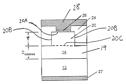
Figure 1 is a cross-sectional view illustrating semiconductor devices
according
to embodiments of the present invention.
Figure 2 is a cross-sectional view illustrating semiconductor devices
according
to additional embodiments of the present invention.
Figure 3 is a cross-sectional view illustrating semiconductor devices
according
to still additional embodiments of the present invention.
CA 02503854 2005-04-26
WO 2004/059706 PCT/US2003/040483
Detailed Description.
The present invention will nov be described more fully hereinafter with
reference to the accompanying drawings, in which preferred embodiments of the
invention are shown. The invention may, however, be embodied in different
forms
, and should not be construed as limited to the embodiments set forth herein.
Rather,
these embodiments are provided so that this disclosure will be thorough and
complete,
and will fully convey the scope of the invention to those skilled in the art.
In the
drawings, the thickness of layers and regions are exaggerated for clarity. It
will also
be understood that when a layer is referred to as being "on" another layer or
substrate,
it can be directly on the other layer or substrate, or intervening layers may
also be
present. It will also be understood that when an element is referred to as
being
"coupled" or "connected" to another element, it can be directly,coupled or
connected
to the other element, or intervening elements may also be present. Like
numbers refer
to like elements throughout. Furthermore, relative terms such as "vertical"
and
"horizontal" rnay be used herein to describe a relationship with respect to a
substrate
or base layer as illustrated in the figures. It will be understood that these
terms are
intended to encompass different orientations of the device in addition to the
orientation depicted in the figures.
As shown in the cross-section of Figure 1, a semiconductor device according
to embodiments of the present invention may include a substrate 12 and an
epitaxial
semiconductor structure 14 including a semiconductor base layer 19 and a
semiconductor mesa 20 on a portion of the base layer 19. More particularly,
the
semiconductor mesa 20 may include a mesa surface 20A opposite the base layer
19,
mesa sidewalls 20B between the mesa surface 20A and the base layer 19, and a
mesa
base 20C adjacent the base layer. While a dashed line is shown between the
semiconductor mesa 20 and the semiconductor base layer 19 for purposes of
illustration, it will be understood that adjacent portions of the
semiconductor base
layer 19 and the semiconductor mesa 20 may comprise a same semiconductor
material with no physical barrier, junction, or discontinuity between the two.
The device may also include a passivation layer 24 on the semiconductor base
layer 19 and on portions of the semiconductor mesa 20 with portions of the
mesa
surface 20A being free of the passivation layer 24. Moreover, a first ohmic
contact
layer 26 may be provided on portions of the mesarsurface 20A free of the
passivation
layer, and a metal overlayer 28 may be provided on the passivation layer 24
and the
CA 02503854 2005-04-26
WO 2004/059706 PCT/US2003/040483
ohmic contact layer 26. In addition, a second ohmic contact layer 27 may be
provided
on the substrate 12 opposite the semiconductor structure 14 to define an
electrical
current path through the mesa 20, the semiconductor base layer 19, and the
substrate
12. In an alternative, a second ohmic contact layer may be provided on a same
side of
5 , the substrate as the epitaxial semiconductor structure 14 so that current
through the
substrate, l2 is not required.
In some embodiments, the substrate 12 may included substrate material such
as N-type silicon carbide having a polytype such as 2H, 4H, 6H, 8H, 15R,
and/or 3C;
sapphire; gallium nitride; and/or aluminum nitride. Moreover, the substrate 12
may
10 be conductive to provide a "vertical" device having a "vertical" current
flow through
the epitaxial semiconductor structure 14 and the substrate 12. In an
alternative, the
substrate 12 may be insulating or semi-insulating where both ohmic contacts
are
provided on a same side of the substrate to provide a "horizontal" device. A
conductive substrate could also be used in a "horizontal" device. Moreover,
the term
substrate may be defined to include a non-patterned portion of the
semiconductor
material making up the semiconductor structure 14, andlor there may not be a
material
transition between the substrate 12 and the semiconductor structure 14.
Portions of the epitaxial semiconductor structure 14 may be patterned into a
mesa stripe, for example, to provide optical and/or current confinement for a
semiconductor laser device. As shown, only a portion of the epitaxial
semiconductor
structure 14 is included in the mesa 20. For example, the epitaxial
semiconductor
structure 14 may include N-type and P-type layers and portions of one or both
of the
N-type and P-type layers may be included in the mesa 20. According to
particular
embodiments, the epitaxial semiconductor structure 14 may include an N-type
layer
adjacent the substrate 12 and a P-type layer on the N-type layer opposite the
substrate
12. The mesa may include portions of the P-type layer and none of the N-type
layer.
In alternatives, the mesa may include all of the P-type layer and portions
(but not all)
of the N-type layer; or all of the P-type layer and all of the N-type layer
(such that
sidewalls of the mesa 20 extend to the substrate 12).
The semiconductor structure 14 may also include a junction between the N-
type and P-type layers. The junction, for example, may be a structural
junction
defined as a physical location in the semiconductor structure 14 where P-type
doping
begins. A structural junction and an actual electronic P-N junction may thus
have
different locations in the semiconductor structure 14 due to reactor effects,
dopant
CA 02503854 2005-04-26
WO 2004/059706 PCT/US2003/040483
11
incorporation rates, dopant activation rates, dopant diffusion, and/or other
mechanisms. '
The epitaxial semiconductor structure 14 may also include an active layer at
the junction between the N-type layer and the P-type layer. The active layer
may
, include a number of different structures and/or layers and/or combinations
thereof.
The active layer, for example, may include single or multiple quantum wells,
double
heterostructures, and/or superlattices. The active layer may also include
light..and/or
current confinement layers that may encourage laser action in the .device.
Moreover,
portions of the active layer may be included in the N-type layer andlor the P-
type
layer adjacent the junction therebetween. According to particular embodiments,
the
active layer may be included in the N-type layer adjacent the junction with
the P-type
layer.
By way of example, a uniformly thick layer of epitaxial semiconductor
material may be formed on the substrate 12, and a layer of an ohmic contact
material
may be formed on the layer of the epitaxial semiconductor material. The
semiconductor mesa 20 and the ohmic contact layer 26 may be formed, for
example,
by selectively etching the layer of the contact material and the layer of the
epitaxial
semiconductor material using a same etch mask, using different etch masks,
and/or
using a lift-off technique. .Methods of forming mesas, contact layers, and
passivation
layers are discussed, for example, in U.S. Application Ser. No. (Attorney
Docket No. 5308-280), in U.S. Application Ser. No. (Attorney Docket
No. 5308-281), and in U.S. Application Ser. No. (Attorney Docket No.
5308-282), the disclosures ofwhich are hereby incorporated herein by
reference.
Exposed portions of the epitaxial semiconductor material can be removed
using a dry etch such as a Reactive Ion Etch (RIE), an Electron Cyclotron
Resonance
(ECR) plasma etch, andlor an Inductively Coupled Plasma (ICP) etch. More
particularly, the epitaxial semiconductor layer can be etched using a dry etch
in an
Argon (Ar) environment with a chlorine (C12) etchant. For example, argon can
flow
at a rate in the range of approximately 2 to 40 sccm and chlorine can flow at
a rate in
the range of approximately 5 to 50 sccm in an RIE reactor at a pressure in the
range of
approximately 5 to 50 mTorr and at an RF power in the range of approximately
200 to
1000 W. These etch parameters are provided by way of example, and other etch
parameters may be used. '
CA 02503854 2005-04-26
WO 2004/059706 PCT/US2003/040483
12
Moreover, thicknesses of the semiconductor base layer 19 and the
semiconductor mesa 20 and a distance of a conductivity junction from the mesa
base
may be determined by an original thickness of the semiconductor layer from
which
the base layer and mesa are patterned, an original depth of the junction in
the
. semiconductor layer, and a depth of an etch used to form the semiconductor
mesa 20.
According to embodiments of the present invention, the mesa etch depth (and
resulting mesa thickness~.may be in the range of approximately 0.1 to 5
microns, and
according to additional embodiments may be no greater than approximately 2.5
microns. In addition, a width of the mesa surface 20A between mesa sidewalls
20B
may be in the range of approximately 1 to 3 microns, and a distance Dsubstrate
from the
mesa base 20C to the substrate can be in the range of approximately 0 to 4.9
microns.
The distance DSU6strate is also a measure of the thickness of the
semiconductor base
layer 19. In addition, the mesa surface 20A may be a P-type semiconductor
material.
The location of the junction in the semiconductor base layer 19 or the
semiconductor mesa 20 can be determined by an original depth of the
conductivity
junction in the semiconductor layer from which the base layer and mesa are
patterned.
If the etch depth of the etch used to form the semiconductor mesa 20 is
greater than a
depth of the junction in the semiconductor layer, the junction can be in
included in the
resulting semiconductor mesa 20. In an alternative, if the etch depth of the
etch used
to form the semiconductor mesa 20 is less than a depth of the junction in the
semiconductor layer, the junction can be included in the semiconductor base
layer 19.
According to particular embodiments, the semiconductor mesa 20 may be
formed such that the. structural junction between N-type and P-type layers is
included
in the semiconductor base layer 19 spaced from the mesa base 20C by a distance
of
no more than approximately 0.4 microns, and more particularly, by a distance
of no
more than approximately 0.2 microns. By providing the structural junction in
the
semiconductor base layer 19 outside the semiconductor mesa 20, beam quality,
stability, and/or voltage characteristics for a resulting semiconductor laser
may be
improved.
In an alternative, the semiconductor mesa 20 may be formed such that the
structural junction between N-type and P-type layers is~included in the
semiconductor
mesa 20 spaced from the mesa base 20C by a distance of no more than
approximately
5 microns, and more particularly, by a distance of no more than approximately
0.75
microns. By providing the structural. junction in the semiconductor mesa 20, a
CA 02503854 2005-04-26
WO 2004/059706 PCT/US2003/040483
13
resulting semiconductor laser may provide stronger guiding and/or improved
operating current characteristics.
. A semiconductor device according to particular embodiments of the present
invention is illustrated in Figure 2. As shown in Figure 2, a semiconductor
device
. may include a substrate 112 and an epitaxial semiconductor structure 114
including a
semiconductor base layer 119 and a semiconductor mesa 120 on a portion of the
base
layer 119. More particularly, the semiconductor mesa 120 may include a mesa
surface 120A opposite the base layer 119, mesa sidewalls 120B between the mesa
surface 120A and the base layer 119, and a mesa base 120C adjacent the base
layer.
While a dashed line is shown between the semiconductor mesa 120 and the
semiconductor base layer 119 for purposes of illustration, it will be
understood that
adjacent portions of the semiconductor base layer 119 and the semiconductor
mesa
120 may comprise a same semiconductor material with no physical barrier,
junction,
or discontinuity between the two.
The device may also include a passivation layer 124 on the semiconductor
base layer 119 and on portions of the semiconductor mesa 120 with portions of
the
mesa surface 120A being free of the passivation layer 124. Moreover,. a first
ohmic
contact layer 126 may be provided on portions of the mesa surface 120A free of
the
passivation layer, and a metal overlayer 128 may be provided on the
passivation layer
124 and the ohmic contact layer 126. In addition, a second ohmic contact layer
127
may be provided on the substrate 112 opposite the semiconductor structure 114
to
define an electrical current path through the mesa 120, the semiconductor base
layer
119, and the substrate 112. In an alternative, a second ohmic contact layer
may be
provided on a same side of the substrate as the epitaxial semiconductor
structure 114
so that current through the substrate 112 is not required.
In some embodiments, the substrate 112 may include a substrate material such
as N-type silicon carbide having a polytype such as 2H, 4H, 6H, 8H, 15I~,
and/or 3C;
sapphire; gallium nitride; and/or aluminum nitride. Moreover, the substrate
112 may
be conductive to provide a "vertical" device having a "vertical" current flow
through
the epitaxial semiconductor structure 114 and the substrate 112. In an
alternative, the
substrate 112 may be insulating or semi-insulating where both ohmic contacts
are
provided on a same side of the substrate to provide a "horizontal" device. A
conductive substrate could also be used in a "horizontal" device. Moreover,
the term
substrate may be defined to include a non-patterned portion of the
semiconductor
CA 02503854 2005-04-26
WO 2004/059706 PCT/US2003/040483
14
material making up the semiconductor structure 114, and/or there may not be a
material transition between the substrate 112 and the semiconductor structure
114.
Portions of the epitaxial semiconductor structure 114 may be patterned into a
mesa stripe, for example, to provide optical and/or current confinement for a
semiconductor laser device. As shown, only a portion of the epitaxial
semiconductor
structure 114 is included in the mesa 120, and the remainder of the epitaxial
semiconductor structure 114 is included in the.~emiconductor base layer 119.
More
particularly, the epitaxial semiconductor structure 114 may include an N-type
layer
115, all of which is included in the semiconductor base layer 119 adjacent the
substrate 112. The epitaxial semiconductor structure 114 may also include a P-
type
layer (including portions 117' and 117") with a junction 122 between the N-
type and
P-type layers. As discussed above, the junction 122 may be a structural
junction
defined as a location where P-type doping begins. A structural junction and an
actual
electronic P-N junction may thus have different locations in the semiconductor
structure 114 due to reactor effects, dopant incorporation rates, dopant
activation
rates, dopant diffusion,.and/or other mechanisms.
As shown in Figure 2, a first portion 117' of the P-type layer is included in
the
semiconductor base layer 119, and a second portion 117" of the P-type layer is
included in the semiconductor mesa 120. A thickness of the first portion 117'
of the
P-type layer is the same as the distance (labeled D'~nn~non) from the mesa
base 120C to
the junction 122 in the semiconductor base layer 119, and the thickness of the
second
portion 117" of the P-type layer (labeled T') is the same as the thickness of
the
semiconductor mesa 120. In addition, a distance D'Snbstrate between the mesa
base
120C and the substrate 112 is the same as a thickness of the semiconductor
base layer
119. Accordingly, a thickness of the N-type layer 115 may be equal to a
difference of
D~substrate minus D'~nnction~
According to particular embodiments, the semiconductor mesa 120 may be
formed such that the junction 122 between N-type and P-type layers is included
in the
semiconductor base layer 119 spaced from the mesa base 120C by a distance
D'~nnction
of no more than approximately 0.4 microns, and more particularly, by a
distance of no
more than approximately 0.2 microns. In addition, the junction 122 may be
included
in the semiconductor base layer 119 spaced from the mesa base 120C by a
distance
D'junction of at least approximately 0.05 microns, and more particularly, the
junction
122 may be included in the semiconductor base layer 119 spaced from the mesa
base
CA 02503854 2005-04-26
WO 2004/059706 PCT/US2003/040483
120C by a distance ~~jUnchon of at least approximately 0:1 microns. By
providing the
structural junction in the semiconductor base layer 119 outside the
semiconductor
mesa 120, beam quality, stability, and/or voltage characteristics for a
resulting
semiconductor laser may be improved.
5 The epitaxial semiconductor structure 114 may also include an active layer
at
the junction 122 between the N-type layer and the P-type layer. The active
layer may
include a number of difFerent structures and/or layers and/or combinations
thereof.
The active layer, for example, may include single or multiple quantum wells,
double
heterostructures, and/or superlattices. The active layer may also include
light and/or
10 current confinement layers that may encourage laser action in the device.
Moreover,
portions of the active layer may be included in the N-type layer and/or the P-
type
layer adjacent the junction therebetween. According to particular embodiments,
the
active layer may be included in the N-type layer 115 adjacent the junction 122
with
the P-type layer.
15 By way of example, a uniformly thick layer of epitaxial semiconductor
material may be formed on the substrate 112, and a layer of an ohmic contact
material
may be formed on the layer of the epitaxial semiconductor material. The
semiconductor mesa 120 and the ohmic contact layer 126 may be formed, for
example, by selectively etching the layer of the contact material and the
layer of the
epitaxial semiconductor material using a same etch mask, using different etch
masks,
and/or using a lift-off technique. Methods of forming mesas, contact layers,
and
passivation _layers are discussed, for example, in U.S~ Application Ser. No.
(Attorney Docket No. 5308-280), in U.S: Application Ser..No. (Attorney
Docket No. 5308-281), and in U.S. Application Ser. No. (Attorney
Docket No. 5308-282), the disclosures of which are hereby incorporated herein
by
reference.
Exposed portions of the epitaxial semiconductor material can be removed
using a dry etch such as a Reactive Ion Etch (RIE), an Electron Cyclotron
Resonance
(ECR) plasma etch, and/or an Inductively Coupled Plasma (ICP) etch. More
particularly, the epitaxial semiconductor layer can be etched using a dry etch
in an
Argon (Ar) environment with a chlorine (Cl2) etchant. For example, argon can
flow
at a rate in the range of approximately 2 to 40 sccm and chlorine can flow at
a rate in
the range of approximately 5 to 50 sccm in an RIE reactor at a pressure in the
range of
approximately S to 50 mTorr and at an RF power in the range of approximately
200 to
CA 02503854 2005-04-26
WO 2004/059706 PCT/US2003/040483
16
1000 W. These etch parameters are provided by way of example, and other etch
parameters may be used.
Moreover, thicknesses of the semiconductor base layer 119 and the
semiconductor mesa 120 and the distance D'~""~no" of the junction 112 from the
mesa
, base 120C may be determined by an original thickness of the semiconductor
layer
from which the base layer 119 and mesa 120 are patterned, an original depth of
the
conductivity junction 122 in the semiconductor layer, and a depth of an Ptch
used to
form the semiconductor mesa 120. According to embodiments of the present
invention, the mesa etch depth (and resulting mesa thickness T') may be in the
range
of approximately 0.1 to 5 microns, and according to additional embodiments may
be
no greater than approximately 2.5 microns. In addition, a width of the mesa
surface
120A between mesa sidewalls 120B may be in the range of approximately 1 to 3
microns, and a distance DS"bstrate from the mesa base 1200 to the substrate
can be in
the range of approximately 0 to 4.9 microns. The distance DS"nstrate is also a
measure
of the thickness of the semiconductor base layer 119. In addition, the mesa
surface
120A may be a P-type semiconductor material.
The location of the junction 122 in the semiconductor base layer 119 can be
determined by an original depth (T' + D!~"nction) of the junction in the
semiconductor
layer from which the base layer and mesa are patterned and an etch depth T'
used to
form the mesa 120. In particular, the etch depth T' of the etch used to form
the
semiconductor mesa 120 can be less than the depth of the junction in the
semiconductor layer so that the junction 122 is included in the semiconductor
base
layer 119.
A semiconductor device according to additional embodiments of the present
invention is illustrated in Figure 3. As shown in Figure 3, a semiconductor
device
may include a substrate 212 and an epitaxial semiconductor structure 214
including a
semiconductor base layer 219 and a semiconductor mesa 220 on a portion of the
base
layer 219. More particularly, the semiconductor mesa 220 may include a mesa
surface 220A opposite the base layer 219, mesa sidewalls 220B between the mesa
surface 220A and the base layer 219, and a mesa base 220C adjacent the base
layer.
While a dashed line is shown between the semiconductor mesa 220 and the
semiconductor base layer 219 for purposes of illustration, it will be
understood that
adjacent portions of the semiconductor base layer 219 and the semiconductor
mesa
CA 02503854 2005-04-26
WO 2004/059706 PCT/US2003/040483
17
220 may comprise a same semiconductor material with no physical barrier,
junction,
or discontinuity between the two.
The device may also include a passivation layer 224 on the semiconductor
base layer 219 and on portions of the semiconductor mesa 220 with portions of
the
mesa surface 220A being free df the passivation layer 224. Moreover, a first
ohmic
contact layer 226 may be provided on portions of the mesa surface 220A free of
the
passivation layer, a.~:d a metal overlayer 228 may be provided on the
passivation layer
224 and the ohmic contact layer 226. In addition, a second ohmic contact layer
227
may be provided on the substrate 212 opposite the semiconductor structure 214
to
define an electrical current path through the~mesa 220, the semiconductor base
layer
219, and the substrate 212. In an alternative, a second ohmic contact layer
may be
provide on a same side of the substrate as the epitaxial semiconductor
structure 214 so
that current through the substrate 212 is not required.
In some embodiments, the substrate 212 may include a substrate material such
as N-type silicon carbide having a polytype such as 2H, 4H, 6H, 8H, 15R,
and/or 3C;
sapphire; gallium nitride; and/or aluminum nitride. Moreover, the substrate
212 may
be conductive to provide a "vertical" device having a "vertical" current flow
through
the epitaxial semiconductor structure 214 and the substrate 212. In an
alternative, the
substrate 212 may be insulating or semi-insulating where both ohmic contacts
are
provided on a same side of the substrate to provide a "horizontal" device. A
conductive substrate could also be used in a "horizontal" device. Moreover,
the term
substrate may be defined to include a non-patterned portion of the
semiconductor
material making up the semiconductor structure 214, and/or there may not be a
material transition between the substrate 212 and the semiconductor structure
214.
Portions of the epitaxial semiconductor structure 214 may be patterned into a
mesa stripe, for example, to provide optical and/or current confinement for a
semiconductor laser device. As shown, only a portion of the epitaxial
semiconductor
structure 214 is included in the mesa 220, and the remainder of the epitaxial
semiconductor structure 214 is included in the semiconductor base layer 219.
More
particularly, the epitaxial semiconductor structure 214 may include a P-type
layer
217, all of which is included in the semiconductor mesa 220 adjacent the mesa
surface
220A. The epitaxial semiconductor structure 214 may also include an N-type
layer
(including portions 215' and 215") with a junction 222 between the P-type
layer and
the N-type layer. As discussed above, the junction 222 may be a structural
junction
CA 02503854 2005-04-26
WO 2004/059706 PCT/US2003/040483
18
defined as a location where P-type doping begins. A structural junction and an
actual
electronic P-N junction may thus have different locations in the semiconductor
structure 114 due to reactor effects, dopant incorporation rates, dopant
activation
rates, dopant diffusion, and/or other mechanisms.
As shown in Figure 3, a first portion 215' of the N-type layer is included in
the
semiconductor base layer 219, and a second portion 215" of the N-type layer is
included in the semiconductor mesa 220. A thickness of the first portion 215'
of the
N-type layer is the same as the distance (labeled D"S"bstr~te) from the mesa
base 220C
to the substrate 212, and the thickness of the second portion 215" of the N-
type layer
(labeled D"~"n~t~o~) is the same as the distance from the mesa base 220C to
the
junction between the N-type and P-type layers. In addition, the thickness of
the
r semiconductor mesa is labeled T". Accordingly, a thickness of the P-type
layer 217
may be equal to a difference of the mesa thickness T" minus D"j"nction.
According to particular embodiments, the semiconductor mesa 220
may be formed such that the junction 222 between N-type and P-type layers is
included in the mesa 220 spaced apart from the mesa base 220C by a distance
D"junction of no more than approximately 5 microns, and more particularly, by
a
distance of no more than approximately 0.75 microns. In addition, the junction
222
may be included in the semiconductor mesa 220 spaced from the mesa base 220C
by
a distance D"~"ncc~on of at least approximately 0.05 microns, and more
particularly, the
junction 222 may be included in the semiconductor mesa 220 spaced from the
mesa
base 2200 by a distance D!'~"n~no" of at least approximately 0.1 microns. By
providing the structural junction in the semiconductor mesa 220 outside the
semiconductor mesa 220, a resulting semiconductor laser may provide stronger
guiding andlor improved operating current characteristics.
The epitaxial semiconductor structure 214 may also include an active layer at
the junction between the N-type layer and the P-type layer. The active layer
may
include a number of different structures and/or layers and/or combinations
thereof.
The active layer, for example, may include single or multiple quantum wells,
double
heterostructures, and/or superlattices. The active layer may also include
light and/or
current confinement layers that may encourage laser action in the device.
Moreover,
portions of the active layer may be included in the N-type layer and/or the P-
type
layer adjacent the junction therebetween. According to particular embodiments,
the
CA 02503854 2005-04-26
WO 2004/059706 PCT/US2003/040483
19
active layer may be included in the second portion 215" of the N-type layer
adjacent
the junction 222 with the P-type layer 217.
By way of example, a uniformly thick layer of epitaxial semiconductor
material may be formed on the substrate 212, and a layer of an ohmic contact
material
, may be formed on the layer of the epitaxial semiconductor material. The
semiconductor mesa 220 and the ohmic contact layer 226 may be formed, for
example, by selectively etching the layer of the contact material and the
layer of the
epitaxial semiconductor material using a same etch mask, using different etch
masks,
and/or using a lift-off technique. Methods of forming mesas; contact layers,
and
passivation layers are discussed, for example, in U.S. Application Ser. No.
(Attorney Docket No. 5308-280), in U.S. Application Ser. No. (Attorney
Docket No. 5308-281), and in U.S. Application Ser. No. (Attorney
Docket No. 5308-282), the disclosures of which are hereby incorporated herein
by
reference.
Exposed portions of the epitaxial semiconductor material can be removed
using a dry etch such as a Reactive Ion Etch (RIE), an Electron Cyclotron
Resonance
(ECR) plasma etch, and/or an Inductively Coupled Plasma (ICP) etch. More
particularly, the epitaxial semiconductor layer can be etched using a dry etch
in an
Argon (Ar) environment with a chlorine (Cl2) etchant. For example, argon can
flow
at a rate in the range of approximately 2 to 40 stem and chlorine can flow at
a rate in
the range of approximately 5 to 50 stem in an RIE reactor at a pressure in the
range of
approximately 5 to 50 mTorr and at an RF power in the range of approximately
200 to
1000 W. These etch parameters are provided by way of example, and other etch
parameters may be used.
Moreover, thicknesses of the semiconductor base layer 219 and the
semiconductor mesa 220 and a distance ~"junction of a junction from.the mesa
base
220C may be determined by an original thickness of the semiconductor layer
from
which the base layer 219 and mesa 220 are patterned, an original depth of the
junction
in the semiconductor layer, and a depth of an etch used to form the
semiconductor
mesa 220. According to embodiments of the present invention, the mesa etch
depth
(and resulting mesa thickness T") may be in the range of approximately 0.1 to
5
microns, and according to additional embodiments may be no greater than
approximately 2.5 microns. In addition, a width of the mesa surface 220A
between
mesa sidewa.lls 220B may be in the range of approximately 1 to 3 microns, and
a
CA 02503854 2005-04-26
WO 2004/059706 PCT/US2003/040483
distance DS"bscrate from the mesa base 220C to the substrate can be in the
range of
approximately 0 to 4.9 microns. The distance Dsubsc~ate is also a measure of
the
thickness of the semiconductor base layer 219. In addition, the mesa surface
220A
may be a 1'-type semiconductor material.
5 , The location of the junction 222 in the semiconductor mesa 220 can be
determined by an original depth (T" - D"~""ct~on) of the junction in the
semiconductor
layer from which the base layer 219 and mesa 220 are patterned and an etch
depth
used to form the mesa 220. In particular, the etch depth T" of the etch used
to form
the semiconductor mesa 220 can be greater than a depth of the junction in the
10 semiconductor layer so that the junction can be included in the
semiconductor base
layer 219.
The resulting semiconductor devices may provide edge emitting
semiconductor lasers with light being emitted parallel to the substrate along
a
lengthwise direction of a semiconductor mesa stripe. Stated in other words,
the light
15 may be emitted along a direction perpendicular to the cross section of the
Figures
discussed above. While methods and devices have been discussed with reference
to
methods of forming light emitting devices such as laser diodes, methods
according to
embodiments of the present invention may be used to form other semiconductor
devices such as conventional diodes, conventional light emitting diodes, or
any other
20 semiconductor device including a semiconductor mesa.
While this invention has been particularly shown and described with reference
to preferred embodiments thereof, it will be understood by those skilled in
the art that
various changes in form and details may be made therein without departing from
the
spirit and scope of the invention as defined by the appended claims and their
equivalents.