Note: Descriptions are shown in the official language in which they were submitted.
CA 02504023 2005-04-13
., 1
SEMICONDUCTOR LIGH~EMITTING DEVICE
BACKGROUND OF THE INVENTION
Field of the Invention
The present invention relates to semiconductor light-emitting devices.
Description of the Background Art
The development in recent years of relatively short-wavelength
semiconductor light-emitting devices, including blue light-emitting diodes
(LEDs) and ultraviolet LEDs, has been flourishing. Group III-V compounds
such as InGaN and AIGaN as well as Group II-VI compounds such as ZnO,
materials of comparatively large band gap, are ideally suited for use in such
semiconductor light-emitting devices. In one example of a semiconductor
light-emitting device of this sort, an active layer containing InGaN is
arranged
in between an rrtype cladding layer containing AlGaN, and a p-type cladding
layer likewise containing AlGaN. In another example, an active layer
containing Zn0 is arranged in between an n-type cladding layer containing
MgZnO, and a p-type cladding layer likewise containing MgZnO.
Crystals composed of a III-V compound like InGaN, or a II-VI compound
like Zn0 in many cases constitute hexagonal structures. In semiconductor
light-emitting devices having active layers composed of such hexagonal-system
crystalline compounds, the generation of spontaneous electric fields, such as
piezoelectric fields, at the active layer heterointerfaces is known to occur.
The
larger such spontaneous electric fields are, the narrower the overlapping
CA 02504023 2005-04-13
,. 2
portions of the wave functions of the electrons and holes in the active layer
become, lowering the probability that the electrons and holes will recombine.
The light-emitting efficiency of such devices consequently deteriorates to the
extent that spontaneous electric fields grow larger. Inasmuch as spontaneous
electric fields become more extensive the thicker is an active layer, the
thickness of active layers (especially well layers in quantum-well structures)
is
restricted for the sake of curbing degradation in light-emitting efficiency
due to
spontaneous electric fields. This limitation on the thickness of active layers
is
one factor impeding the enhancement of semiconductor light-emitting device
brightness.
SUMMARY OF THE INVENTION
An object of the present invention, having been brought in consideration
of the foregoing issues, is to make available semiconductor light-emitting
devices in which generation of spontaneous electric fields in the active layer
is
reduced to enable enhanced brightness.
In order to resolve the problems discussed above, a semiconductor
light-emitting device according to the present invention is furnished with: a
semiconductor layer of a first conductivity type, composed of a hexagonal
compound a semiconductor layer of a second conductivity type, composed of a
hexagonal compound and provided over the first-conductivity-type
semiconductor layer and an active layer, composed of a hexagonal compound
and provided in between the first-conductivity-type semiconductor layer and
CA 02504023 2005-04-13
.~ 3
the second-conductivity-type semiconductor layer. The semiconductor
light-emitting device is therein characterized in that the angles that an axis
orthogonal to the active-layer interface on its first-conductivity-type
semiconductor layer side, and an axis orthogonal to the active-layer interface
on
its second-conductivity-type semiconductor layer side respectively form with
the taxis in the active layer are greater than zero.
A semiconductor light-emitting device according to another aspect of the
present invention is furnished with: a nitride semiconductor layer of a first
conductivity type a nitride semiconductor layer of a second conductivity type,
provided over the first-conductivity-type nitride semiconductor layer and an
active layer provided in between the first-conductivity-type nitride
semiconductor layer and the second-conductivity-type nitride semiconductor
layer, and composed of a nitride. The semiconductor light-emitting device is
therein characterized in that the angles that an axis orthogonal to the
active-layer interface along the first-conductivity-type nitride semiconductor
layer, and an axis orthogonal to the active-layer interface along the
second-conductivity-type nitride semiconductor layer respectively form with
the
c~axis in the active layer are greater than zero.
In an implementation in which the active layer is composed of a
hexagonal compound such as a nitride semiconductor, spontaneous electric
fields that occur in the active layer will be largest when the axes orthogonal
to
the two boundary surfaces flanking the active layer coincide with the taxis in
the active layer (that is, when the active layer grows on the cplane). In
either of
CA 02504023 2005-04-13
., .. 4
the semiconductor light-emitting devices described above, the fact that the
angles that an axis orthogonal to the active-layer interface along the
first-conductivity-type semiconductor layer (or the first-conductivity-type
nitride semiconductor layer), and an axis orthogonal to the active-layer
interface along the second-conductivity-type semiconductor layer (or the
second-conductivity-type nitride semiconductor layer) respectively form with
the c-axis in the active layer are greater than zero (that is, the fact that
the two
boundary surfaces flanking the active layer are not cplanes), contributes to
reducing the generation of spontaneous electric fields in the active layer.
Since
thus reducing spontaneous electric fields broadens the overlapping portions of
the wave functions of the electrons and holes in the active layer, raising the
likelihood that the electrons and holes will recombine, the active layer may
be
made thicker, which enables the brightness of the light-emitting device to be
enhanced to a greater degree.
A semiconductor light-emitting device according to a further aspect of the
invention is furnished with: a substrate composed of a hexagonal compound and
having a principal face a semiconductor layer of a first conductivity type,
composed of a hexagonal compound and grown epitaxially onto the principal
face of the substrate an active layer grown epitaxially onto the
first-conductivity-type semiconductor layer and composed of a hexagonal
compound and a semiconductor layer of a second conductivity type, composed
of a hexagonal compound and grown epitaxially onto the active layer. The
semiconductor light-emitting device is therein characterized in that the angle
CA 02504023 2005-04-13
,. .. 5
that an axis orthogonal to the principal face of the substrate forms with the
maxis of the substrate is greater than zero.
In accordance with a still further aspect of the invention a semiconductor
light-emitting device is furnished with: a substrate composed of a Group III
nitride and having a principal face a nitride semiconductor layer of a first
conductivity type, grown epitaxially onto the principal face of the nitride
substrate an active layer grown epitaxially onto the first-conductivity-type
nitride semiconductor layer, and composed of a nitride and a nitride
semiconductor layer of a second conductivity type, grown epitaxially onto the
active layer. The semiconductor light-emitting device is therein characterized
in
that the angle that an axis orthogonal to the principal face of the nitride
substrate forms with the c~axis of the nitride substrate is greater than zero.
In either of the semiconductor light-emitting devices described above, the
fact that the angle that an axis orthogonal to the principal face of the
substrate
(or the nitride substrate) forms with the taxis of the substrate (or the
nitride
substrate) is greater than zero (that is, the fact that the principal face of
the
substrate (or the nitride substrate) is not a cplane) means that the two
boundary surfaces of the active layer grown epitaxially onto the principal
face
are not cplanes, therefore making it possible to reduce the generation of
spontaneous electric fields in the active layer. Thus reducing spontaneous
electric fields allows the active layer may be made thicker, which enables the
brightness of the light-emitting device to be enhanced to a greater degree.
The foregoing semiconductor light-emitting devices may also be
CA 02504023 2005-04-13
characterized in that the principal face of the substrate (or the nitride
substrate) contains any one plane among the {1010} planes, {112 4} planes, and
{112 0} planes of the substrate (or the nitride substrate). In that this will
mean
that the two boundary surfaces of the active layer contain any one plane among
these planes, the generation of spontaneous electric fields in the active
layer
can be reduced effectively It will be appreciated that {1010} planes, {112 4}
planes, and {112 0} planes as used herein signify families of equivalent
planes.
For example, the (1010) plane, the (0110) plane, the (1100) plane, the (1010)
glane, the (0110) plane, and the (1100) plane would be included in the {1010}
family of planes.
The foregoing semiconductor light-emitting devices may be characterized
in being further furnished with a first electrode, provided on the reverse
face of
the substrate (or nitride substrate) and in ohmic contact with the substrate
(or
nitride substrate), and a second electrode, provided on the
second-conductivity-type semiconductor layer (or the second-conductivity-type
nitride semiconductor layer) and in ohmic contact with the
second-conductivity-type semiconductor layer (or the second-conductivity-type
nitride semiconductor layer). Providing electrodes on the two faces of the
semiconductor light-emitting device in this way makes for very efficient
injecting of electrons and holes into the active layer, thus contributing to
brightness-enhancing the semiconductor light-emitting device further.
Semiconductor light-emitting devices in aspects of the present invention
set forth above may also be characterized in that the hexagonal compounds of
CA 02504023 2005-04-13
, 'l
the first-conductivity-type semiconductor layer, the second-conductivity-type
semiconductor layer, and the active layer include Group II atoms and Group VI
atoms. The fact that, inasmuch as crystals of II-VI compounds containing
Group II atoms and Group VI atoms will constitute hexagonal crystalline
structures, the angles that an axis orthogonal to the active-layer interface
along
the first-conductivity-type semiconductor layer, and an axis orthogonal to the
active-layer interface along the second-conductivity-type semiconductor layer
respectively form with the taxis in the active layer will be greater than
zero,
contributes to efficiently reducing the generation of spontaneous electric
fields
in the active layer. Semiconductor light-emitting devices in these
implementations may be characterized in that the Group II atoms are zinc
atoms, or characterized in that the hexagonal compounds are Zn0-based
compounds.
Alternatively, semiconductor light-emitting devices in certain aspects of
the invention may be characterized in that the hexagonal compounds of the
first-conductivity-type semiconductor layer, the second-conductivity-type
semiconductor layer, and the active layer include Group III atoms and Group V
atoms. The fact that, inasmuch as crystals of III-V compounds containing
Group III atoms and Group V atoms will constitute hexagonal crystalline
structures, the angles that an axis orthogonal to the active-layer interface
along
the first-conductivity-type semiconductor layer, and an axis orthogonal to the
active-layer interface along the second-conductivity-type semiconductor layer
respectively form with the c-axis in the active layer will be greater than
zero,
CA 02504023 2005-04-13
. .
contributes to efficiently reducing the generation of spontaneous electric
fields
in the active layer. Semiconductor light-emitting devices in these
implementations may be characterized in that the Group V atoms are nitrogen
atoms, or characterized in that the hexagonal compounds are GaN-based
compounds.
Furthermore, semiconductor light-emitting devices in relevant aspects of
the present invention may be characterized in that dislocation density in the
principal face of the nitride substrate is 1 x 108 cm 2 or less. By thus
furnishing
the semiconductor light-emitting devices with a nitride substrate in which the
dislocation density in the principal face is comparatively small, the density
of
dislocations that, penetrating the first-conductivity-type nitride
semiconductor
layer, reach the active layer can be held low to further heighten the
light-emitting efficiency of the devices.
In addition, semiconductor light-emitting devices of the present
invention may be characterized in that the active layer has a quantum-well
structure that includes a well layer and, flanking the well layer, barrier
layers
that set up a potential barrier in the well layer, with the thickness of the
well
layer being greater than 3 nm. On account of the occurrence of spontaneous
electric fields as discussed earlier, the well-layer thickness in a quantum-
well
structure has traditionally been restricted to being no greater than 3 nm. In
contrast, the fact that incidents of spontaneous electric fields in the well
layer
can be reduced by means of the foregoing semiconductor light-emitting devices
enables the well layer to be made thicker than what has conventionally been
CA 02504023 2005-04-13
. g
the case.
Semiconductor light-emitting devices of the present invention may
further be characterized in that the well layer is composed of AlxInyGa(i_x-
y)N (0
<_ x <_ 1, 0 < y <_ 1). In conventional devices in which the well layer thus
includes
indium (In) in their composition, the larger the atomic fraction of In, the
more
pronounced will be the occurrences of spontaneous electric fields. In
contrast,
the fact that incidents of spontaneous electric fields in the well layer can
be
reduced by means of the semiconductor light-emitting devices in each of the
foregoing aspects of the present invention enables enhanced brightness even in
semiconductor light-emitting devices furnished with a well layer composed of
AlxInyGa(i-x-y>N (0 <_ x <_ 1, 0 < y <_ 1).
By means of semiconductor light-emitting devices according to the
present invention, outbreaks of spontaneous electric fields in the active
layer
are minimized to enable enhanced brightness.
From the following detailed description in conjunction with the
accompanying drawings, the foregoing and other objects, features, aspects and
advantages of the present invention will become readily apparent to those
skilled in the art.
BRIEF DESCRIPTION OF THE DRAWINGS
Fig. 1 is a drawing illustrating a semiconductor light-emitting device
involving an embodiment of the present invention
Fig. 2 is isometric views illustrating a substrate in this embodiment,
CA 02504023 2005-04-13
. . . 10
wherein Fig. 2B is a diagram for explaining crystal orientation in the
substrate
depicted in Fig. 2A~
Fig. 3 is a sectional view of the semiconductor light-emitting device from
a lateral perspective, for explaining in further detail an active layer in
this
embodiment
Figs. 4A-4C are sectional views for explaining a method of
manufacturing a substrate for this embodiment
Figs. 5A-5C are sectional views for explaining a method utilizing the
substrate to manufacture the semiconductor light-emitting device and
Fig. 6 is a chart setting forth residual electron densities within MgZnO
not having been doped, and p-type carrier concentration within MgZnO having
been nitrogen-doped, in cases in which MgZnO crystal has been grown onto a
{0001} plane, onto a {1010} plane, and onto a {112 4} plane, respectively
DETAILED DESCRIPTION OF THE INVENTION
While referring to the accompanying drawings, a detailed explanation of
embodiments of semiconductor light-emitting devices according to the present
invention will be made in the following. It should be understood that in
discussing the drawings, with identical reference marks being attached to
identical elements, redundant description of such elements will be omitted.
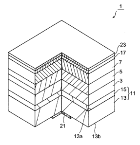
Fig. 1 is a drawing representing a semiconductor light-emitting device
involving an embodiment of the present invention. The semiconductor
light-emitting device illustrated in Fig. 1 is an optimal structure for a
CA 02504023 2005-04-13
' ' 11
planar-emitting optical element such as a light-emitting diode.
As will be seen in Fig. 1, the semiconductor light-emitting device 1 is
furnished with a support base 11, an n-type cladding layer 3, an active layer
5, a
p-type cladding layer 7, a p-type contact layer 17, a cathode 21, and an anode
23.
The support base 11 is constituted to include a substrate 13, and an
n-type buffer layer 16 grown epitaxially onto the principal face 13a of the
substrate 13. With the n-type buffer layer 15 intervening, the n-type cladding
layer 3, active layer 5, p-type cladding layer 7, and Ftype contact layer 17
are
laminated in order onto the principal face 13a of the substrate 13. The
substrate
13 is constituted to include a hexagonal compound such as a III-V compound
containing Group III atoms and Group V atoms, or a II-VI compound
containing Group II atoms and Group VI atoms. As specific examples, a nitride
substrate composed of a Group III nitride (e.g., a gallium-nitride (GaN) based
compound or an aluminum-nitride (A1N) based compound) containing nitrogen
atoms (N) as Group V atoms, or a substrate composed of a compound (e.g., a
zinc-oxide (Zn0) based compound) containing zinc atoms (Z) as Group II atoms
can be utilized as the substrate 13.
The substrate 13 is lent a rectangular plate form in which for example,
its thickness is 300 ,pan, and its planar dimensions are 10 mm x 10 mm.
Another
characteristic of the substrate 13 is that it has n-type conductivity from the
addition of an n-type dopant such as silicon (Si) for example. An optimal
concentration of n-type dopant in the substrate 13 is for example from 1 x 101
CA 02504023 2005-04-13
. , . 12
cm 3 to 1 x 1019 cm g. Further, so that light generated in the active layer 5
will
pass optimally through the substrate 13, the absorption coefficient of the
substrate 13 with respect to light of wavelengths from 450 nm to 750 nm is
preferably from 2 crri 1 to 100 cm 1
Tb illustrate, Fig. 2A is an isometric view depicting the substrate 13 in
the present embodiment, and Fig. 2B is a diagram for explaining crystal
orientation in the substrate 13 as depicted in Fig. 2A. The principal face 13a
of
the substrate 13 in the present embodiment is fashioned so that the angle
formed by an axis A perpendicular to at least a portion of the principal face
13a,
and a direction, in terms of the unit cells of the substrate 13 lattice, along
the
c-axis (that is, a <0001> direction) will be greater than zero. In particular,
the
principal face 13a preferably is formed so that, as illustrated in Fig. 2B,
the axis
A runs in a <1010> direction in substrate 13 unit cells. Put in different
terms, at
least a portion of the principal face 13a of the substrate 13 preferably
contains a
{1010} plane (plane 31 in Fig. 2B) in substrate 13 unit cells. It should be
understood that as stated herein, "contains a {1010} plane" is not limited to
implementations in which at least a portion of the principal face 13a
coincides
strictly with a {1010} plane for example, as long as the absolute value of the
angle formed by a {1010} plane and at least a portion of the principal face
13a is
10° or less, operational performance nearly equal to that of an
implementation
in which at least a portion of the principal face 13a coincides exactly with a
{1010} plane can be achieved.
Alternatively, the principal face 13a preferably is fashioned so that the
CA 02504023 2005-04-13
13
axis A runs in a <112 4> direction or a <112 0> direction in terms of the unit
cells of the substrate 13 lattice. Put in different teams, at least a portion
of the
principal face 13a of the substrate 13 preferably contains a {ll 2 4] plane or
a
{ll 2 0~ plane in substrate 13 unit cells.
A further preference in the present embodiment is that the lattice
constant of the substrate 13 along the c~axis (i.e., in the [0001] direction)
be
within a 5.1851 ~0.0005 t~ range, with the constant on the a1 axis ([2110]
direction) or on the as axis ([ 1210] direction) or on the a3 axis ([ 1120]
direction)
being within a 3.1891 ~0.0005 !~ range. Alternatively, it is preferable that
the
full width at half maximum (FWHM) of an X-ray rocking curve measuring, by
X-ray diffraction analysis, a unit surface area (1 mm x 1 mm) in the principal
face 13a of the substrate 13 be 1000 arcseconds or less. A substrate 13
furnishing any of the distinguishing features described above may be termed a
substrate 13 of excellent crystalline properties. Such a substrate 13,
moreover,
is optimally realized by a manufacturing method to be described later.
A further preference is that in implementations in which the substrate 13
is a nitride substrate composed of a Group III nitride, the dislocation
density in
the principal face 13a of the substrate 13 be a comparatively small value,
such
as 1 x 10⁸ cva 2. Again, such a substrate 13 is optimally realized by a
manufacturing method to be described later. Holding the dislocation density in
the principal face 13a of the substrate 13 down relatively low allows the
density
of "pipe" dislocations that form in the active layer 5 and act as nonradiative
centers to be reduced.
CA 02504023 2005-04-13
. ~ ~ 14
The n-type buffer layer 15 is constituted to include the same material as
does the substrate 13, namely, a hexagonal compound such as a III-V
compound containing Group III atoms and Group V atoms or a II-VI compound
containing Group II atoms and Group VI atoms, to which has been added an
n-type dopant such as Si.
Reference is again made to Fig. 1. The n-type cladding layer 3 is in the
present embodiment a semiconductor layer of a first conductivity type, and is
constituted to include a hexagonal crystalline semiconductor compound such as
a III-V compound containing Group III atoms and Group V atoms, or a II-VI
compound containing Group II atoms and Group VI atoms. Specifically, the
n-type cladding layer 3 may be a first-conductivity-type nitride semiconductor
layer composed of, for example, a Group III nitride containing nitrogen atoms
(N) as Group V atoms (e.g., a GaN-based compound such as Al=iGai-xiN (0 <- x15
1)), or may be a semiconductor layer composed of a compound containing zinc
16 atoms (Zn) as Group II atoms (e.g., A Zn0-based compound such as MgylZy_y0
(0 <_ yi < 1)). An n-type dopant such as silicon, for example, is added to the
n-type
cladding layer 3. The rrtype cladding layer 3 is grown epitaxially onto the
support base 1.1, that is, onto the n-type buffer layer 15.
The active layer 5 is the light-emitting region in the semiconductor
light-emitting device 1. The active layer 5 is constituted to include a
hexagonal
compound such as a III-V compound containing Group III atoms and Group V
atoms, or a II-VI compound containing Group II atoms and Group VI atoms.
Specifically, active layer 5 is composed of, for example, a Group III nitride
CA 02504023 2005-04-13
containing nitrogen atoms (N) as Group V atoms (e.g., a GaN-based compound
such as AlxInyGaci-x-y)N (0 <_ x <_ 1, 0 < y <_ 1)), or is composed of a
compound
containing zinc atoms (Zn) as Group II atoms (e.g., a Zn0-based compound such
as Zn0 for example). The active layer 5 is grown epitaxially onto the rrtype
5 cladding layer 3.
The p-type cladding layer 7 and the p-type contact layer 17 are in the
present embodiment semiconductor layer of a second conductivity type, and are
constituted to include a hexagonal crystalline semiconductor compound such as
a III-V compound containing Group III atoms and Group V atoms, or a II-VI
10 compound containing Group II atoms and Group VI atoms. Specifically, the
p-type cladding layer 7 may be a second-conductivity-type nitride
semiconductor layer composed of, for example, a Group III nitride containing
nitrogen atoms (N) as Group V atoms (e.g., a GaN-based compound such as
AIXaGai_x2N (0 5 x2 <_ 1)), or may be a semiconductor layer composed of a
15 compound containing zinc atoms (Zri) as Group II atoms (e.g., a Zn0-based
compound such as Mgy2Zni_~O (0 <_ yz < 1)). In implementations in which the
p-type cladding layer 7 contains a III-V compound, magnesium (Mg), for
example, is added as a p-type dopant to the p-type cladding layer 7. Likewise,
in
implementations in which the type cladding layer 7 contains a II-VI
compound, nitrogen (N), for example, is added as a p-type dopant to the p-type
cladding layer 7. The p-type cladding layer 7 is grown epitaxially onto the
active
layer 5. This means that the active layer 6 is sandwiched between the n-type
cladding layer 3 and the p-type cladding layer 7.
CA 02504023 2005-04-13
16
The n-type cladding layer 3 supplies electrons to the active layer 5, while
the p-type cladding layer 7 supplies holes to the active layer 5. Further, by
the
active layer 5 containing AlInGaN or ZnO, and the rrtype cladding layer 3 and
the p-type cladding layer 7 each being composed of AIGaN or MgZnO, the
potential barrier (band gap) of the rrtype cladding layer 3 and the p-type
cladding layer 7 is made higher than the potential barrier of the active layer
5.
Accordingly, the carriers (electrons and holes) supplied to the active layer 5
are
confined to the interior of the active layer 5 by the action of the rrtype
cladding
layer 3 and p-type cladding layer 7, which promotes their recombination in the
active layer 5 for more efficient generation of light.
In this embodiment, inasmuch as the n-type buffer layer 15, the mtype
cladding layer 3, the active layer 5, and the p-type cladding layer 7 are in
order
each grown epitaxially onto the principal face 13a of the substrate 13, the
planar orientation of the boundary surface of the active layer 5 on its n~type
cladding layer 3 side, and of the boundary surface of the active layer 6 on
its
p-type cladding layer 7 side each reflect the planar orientation of the
principal
face 13a. This means that the angle that an axis perpendicular to the active
layer 5 interface with the n-type cladding layer 3, and the angle that an axis
perpendicular to the active layer 5 interface with the p-type cladding layer 7
each form with the course of the maxis in the active layer 5 will be greater
than
zero. For example, if at least a portion of the principal face 13a contains a
{1010}
plane, the two interfaces flanking the active layer 5 will also contain a
{1010}
plane. Here it is preferable that the two interfaces flanking the active layer
5
CA 02504023 2005-04-13
17
contain, as does the principal face 13a, any plane among the f 1010} planes,
{112 4} planes and {ll 2 0} planes in the active layer 5.
The p-type contact layer 17, a layer for electrically connecting the p-type
cladding layer 7 and the anode 23, is composed of a hexagonal crystalline
semiconductor compound to which a p-type dopant has been added. For
example, in the present embodiment the p-type contact layer 17 is composed of
a nitride semiconductor, such as gallium nitride, that has been doped with
magnesium, or of a Zn0-based semiconductor compound, such as zinc oxide,
that has been doped with nitrogen. The p-type contact layer is formed onto the
p-type cladding layer 7.
The cathode 21 is in the present embodiment a first electrode. The
cathode 21 is provided on the reverse face 13b of the substrate 13, and in the
present embodiment the cathode 21 is provided on a single portion (the
approximate central portion) of the substrate 13 reverse face 13b. The cathode
21 is a laminate of a sequence of metals, such as Ti - Al - Au for example,
and
therein realizes an ohmic contact between it and the reverse face 13b of the
substrate 13.
The anode 23 is in the present embodiment a second electrode. The anode
23 is provided atop the p-type contact layer 17, and in the present embodiment
the anode 23 is provided over the entire face of the p-type contact layer 17.
The
anode 23 is a laminate of a sequence of metals, such as Ni - Au - A1 - Au for
example, and therein realizes an ohmic contact between it and the p-type
contact layer 17. In addition, the anode 23 functions to reflect light
generated in
CA 02504023 2005-04-13
18
the active layer 5.
In that regard, in order to give further details of the active layer 5 in the
present embodiment, the description now turns to Fig. 3, a lateral sectional
view of the semiconductor light-emitting device 1. The active layer 5 includes
one or a plurality of well layers (for example, well layers 25a-25c) and a
plurality of barrier layers (for example, barrier layers 27a-27d), as depicted
in
Fig. 3. In the present embodiment, the well layers 25a through 25c are formed
so that the thickness of each of the well layers 25a-25c will be greater than
3
nm.
The well layers 25a-25c are laminated in alternation with the barrier
layers 27a-27d, thus constituting a quantum-well structure in the active layer
5.
In an implementation in which the active layer 5 is composed of a Group III
nitride, the well layers 25a-25c are exemplarily composed of AlxInyGay-x-Y)N
(0
<_ x <_ 1, 0 < y 5 1), and the barrier layers 27a-27d are exemplarily composed
of
AlxsInYSGaci-xs-ys>N (0 <_ xs 5 1, 0 <_ ys < 1). The quantum-well structure is
constituted so that the band gap of the barrier layers 27a-27d will be larger
than the band gap of the well layers 25a-25c, and accordingly the barrier
layers
27a-27d set up a potential barrier in the well layers 25a-25c. It should be
understood that although the active layer 5 in the present embodiment has a
multiple-quantum-well (MfaW) structure, it may instead have a
single-quantum-well (SQW) structure.
A further feature of the active layer 5 is that because the well layers
25a-25c and the barrier layers 27a-27d respectively are epitaxially grown by
CA 02504023 2005-04-13
19
turns, the planar orientations of the interfaces between the well layers 25a-
25c
and the barrier layers 27a-27d each reflect the planar orientation of the
principal face 13a of the substrate 13. This means that the angle that an axis
perpendicular to the interfaces between the well layers 25a-25c and the
barrier
layers 27a-27d forms with the course of the taxes in the well layers 25a-25c
and the barrier layers 27a-27d will be greater than zero. It is preferable
that the
interfaces between the well layers 25a-25c and the barrier layers 27a-27d
contain, as does the principal face 13a, any plane among the {1010} planes,
{112 4} planes and f 112 0} planes.
Herein, in order to achieve comparatively intense brightness with the
semiconductor light-emitting device 1 the surface area of a sectional plane
intersecting the course of the active layer 5 thickness preferably is 0.1 mm2
or
more. And in order to maintain highly afficient emission of light, within the
just-noted sectional surface area in the active layer 5, the surface-area
proportion into which carriers are implanted to make that proportion a
light-emitting region is preferably 90°/ or more.
The operation of a semiconductor light-emitting device 1 having the
foregoing configuration is as follows. A drive voltage is applied across the
anode
23 and the cathode 21, whereupon electrons and holes concentrate in the well
layers 25a-25c inside the active layer 5. Then, by the electrons and holes
recombining within the well layers 25a-25c, light is produced. Among the light
generated in the active layer 5, rays directed toward the anode 23 are
reflected
at the anode 23, and the light is then output to the exterior of the
semiconductor
CA 02504023 2005-04-13
light-emitting device through the reverse face 13b of the substrate 13.
At this point, a method of manufacturing a semiconductor light-emitting
device 1 of the present embodiment as described in the foregoing will be
explained. Reference is made to Figs. 4A-4C, sectional views for explaining a
5 method of manufacturing a substrate 13 (cf. Fig. 2A). of the present
embodiment,
and to Figs. 5A-5C, sectional views for explaining a method of manufacturing a
semiconductor light-emitting device 1 utilizing the substrate 13. It should be
understood that although an implementation in which the substrate 13 is
composed of gallium nitride (GaN) will be detailed in the description below,
10 implementations in which the substrate 13 is composed of aluminum nitride
(A1N) are also manufacturable by the same method as below.
At first, a GaAs wafer 41 with its principal face 41a being a X111} plane,
as is represented in Fig. 4A, is readied. Then, by a technique, which will be
explained below, called epitaxial lateral overgrowth (ELO), GaN is grown onto
15 the principal face 41a of the GaAs wafer. In the ELO, initially a mask 43
having
windows is formed on the principal face 41a of the GaAs wafer 41. A substance
on which GaN will not directly grow should be utilized as the material for the
window-perforated mask 43.
The manufacturing method continues by epitaxially growing GaN on the
20 principal face 41a of the GaAs wafer 41, through the windows in the
perforated
mask 43, whereby a GaN ingot 45 is formed. The GaN grows along the taxis in
the process. And although crystal defects (dislocations, etc.) originating in
lattice mismatch between GaAs and GaN are produced in the process, because
CA 02504023 2005-04-13
21
the GaN after growing directly over the GaAs wafer 41 grows on the perforated
mask 43, in a direction paralleling the principal face 41a, the crystal
defects
also grow in the same direction. The crystal defects then gather in locations
in
which neighboring instances of GaN having grown in the direction paralleling
the principal face 41a collide, becoming planar defects. The fact that crystal
defects that arise scattered in the GaN interior are in this way concentrated
into planar defects by ELO contributes to optimally obtaining a GaN ingot 45
of
low dislocation density, in which the dislocation density might be 1 x 10⁸
crri 2,
for example.
The method then proceeds by cutting GaN wafers 47 off of the GaN ingot
45. In the process, slicing so that for example the principal face 47a of the
GaN
wafers 47 will be parallel to the course of the c-axis in the GaN ingot
enables
GaN wafers 47 that contain a {1010} plane or a {ll 2 0} plane in the principal
face 47a to be optimally obtained (Fig. 4C). Alternatively, slicing so that
for
example the principal face 49a of GaN wafers 49 diagonally intersects the
course of the taxis in the GaN ingot 45 enables GaN wafers 49 that contain a
{112 4} plane in the principal face 49a to be optimally obtained. Here, in the
description below, the situation in which GaN wafers 47 containing a {1010}
plane in the principal face 47a are sliced off the ingot will be detailed.
The method then continues by epitaxially growing, as shown in Fig. 5A,
an n-type buffer layer 51, an n-type cladding layer 53, an active layer 55, a
p-type cladding layer 57, and a p-type contact layer 59 in order onto the
principal face 47a of the GaN wafer 47. These layers are of the same materials
CA 02504023 2005-04-13
22
as the previously described materials of the n-type buffer layer 15, the
rrtype
cladding layer 3, the active layer 5, the p-type cladding layer 7, and the p-
type
contact layer 17, respectively. This epitaxial growth is followed by the
formation
of an anode 61, as shown in Fig. 5B, onto the p-type contact layer 59 by a
process such as vapor deposition. In turn, a mask of a predetermined pattern
is
wrought onto the reverse face 47b of the GaN wafer 47, where a plurality of
cathodes 21 is formed by vapor-deposition of a cathode material and subsequent
removal of the mask.
In the next stage, the GaN wafer 47 and the overlying layers are cleaved
through their thickness to complete a semiconductor light-emitting device 1
furnished with a substrate 13 made of GaN, an n-type buffer layer 15, an n-
type
cladding layer 3, an active layer 5, a p-type cladding layer 7, a p-type
contact
layer 17, an anode 23, and a cathode 21.
In implementations in which the substrate 13 is composed of zinc oxide
(Zn0), although the way that the ingot is grown will differ from that when the
substrate is composed of gallium nitride, a semiconductor light-emitting
device
1 may be manufactured by a method that is the same as the foregoing
manufacturing method from the stage in which wafers are sliced from the ingot.
In such implementations, initially zinc oxide (Zn0) wafers are sliced from
electroconductive Zn0 crystal. In the process of doing so, slicing so that for
example the principal face of the Zn0 wafer will be parallel to the course of
the
c~axis in the Zn0 crystal enables Zn0 wafers that contain a ~1010~ plane or a
f 112 0) plane in the principal face to be obtained. Alternatively, slicing so
that
CA 02504023 2005-04-13
23
for example the principal face of the Zn0 wafers diagonally intersects the
course of the taxis in the Zn0 crystal enables Zn0 wafers that contain a {112
4}
plane in the principal face to be obtained.
In this implementation, the method then continues by utilizing
molecular-beam epitaxy to grow in order an n-type buffer layer composed of
n-type ZnO, and an n-type cladding layer composed of n-type MgZnO, each at a
thickness of from 10 nm to 1000 nm, onto the Zn0 wafer, thereon to grow an
active layer composed of undoped ZnO, at a thickness of from 1 nm to 10 nm,
and thereon to grow in order a p-type buffer layer composed of p-type MgZnO,
and a p-type contact layer composed of ZnO, each at a thickness of from 10 nm
to 1000 nm. Ohmic electrodes are then formed respectively on the reverse face
of the Zn0 wafer, and on the p-type contact layer, and the Zn0 wafer and the
layers on the Zn0 wafer are cleaved through their thickness to complete a
semiconductor light-emitting device.
Performance of a semiconductor light-emitting device 1 according to the
present embodiment as described in the foregoing will be explained. Ordinarily
in manufacturing a Group-III nitride semiconductor or a Zn0-based
semiconductor, in most cases the semiconductor layers such as the active layer
are grown onto the c-face of the substrate. This is because for the
crystal-surface planarity and the device photoluminescence characteristics,
growing Group III nitrides or Zn0-based compounds along the c~axis is
preferable.
Nevertheless, in instances in which an axis orthogonal to the two
CA 02504023 2005-04-13
24
interfaces (heterointerfaces) flanking the active layer and the c~axis in the
active layer coincide (that is, in instances in which the active layer has
been
grown onto the cplane), spontaneous electric fields, such as piezoelectric
fields,
produced in the heterointerfaces of the active layer become maximal. In a
semiconductor light-emitting device 1 according to the present embodiment, the
active layer 5 is formed so that the angle that an axis orthogonal to the
interface
of the active layer 5 with the n-type cladding layer 3, and the angle that an
axis
orthogonal to the interface of the active layer 5 with the p-type cladding
layer 7
each make with the taxis in the active layer 5 will be greater than zero (that
is,
so that the two heterointerfaces flanking the active layer 5 will not be
cplanes).
This contributes to reducing spontaneous electric fields occurring in the
active
layer 5. The fact the overlapping portions of the wave functions of the
electrons
and holes in the active layer 5 are thus broadened, raising the likelihood
that
the electrons and holes will recombine, paves the way to making the active
layer 5 thicker than what has been conventional, which enables the brightness
of the light-emitting device to be enhanced.
A further feature of a semiconductor light-emitting device 1 according to
the present embodiment is that the principal face 13a of the substrate 13 is
fashioned so that the angle formed by an axis A (cf. Figs. 2A and 2B)
orthogonal
to the principal face 13a, and the c~axis of the substrate 13 will be larger
than
zero (that is, so that the principal face 13a of the substrate 13 will not be
a
plane). Consequently, the fact that the two heterointerfaces of the active
layer
5 grown epitaxially onto the principal face 13a will not be cplanes makes
CA 02504023 2005-04-13
possible the reduction of spontaneous electric fields occurring in the active
layer
5. This also enables the active layer 5 to be made thicker than usual, which
provides for enhancing the brightness of the semiconductor light-emitting
device.
5 What is more, the present inventors discovered that with II-VI
compounds, crystals grown in a direction other than the c~axis direction
yielded
better semiconductor characteristics than II VI crystals grown with the course
of the taxis as the growth direction. In this regard, reference is made to
Fig. 6,
which is a chart setting forth residual electron densities within MgZnO not
10 having been doped, and p-type carrier concentration within MgZnO having
been nitrogen-doped, in cases in which MgZnO crystal was grown onto a {0001}
plane, onto a {1010} plane, and onto a {ll 2 4} plane, respectively. From Fig.
6 it
will be understood that in the instance in which MgZnO crystal was grown onto
a {0001} plane (that is, in an instance in which Zn0 crystal was grown with
the
15 course of the taxis as the growth direction), with the MgZnO not having
been
doped the residual electron density was a large 5 x 1016 cm 3, moreover, with
the
MgZnO having been nitrogen-doped the p-type carrier concentration was
unmeasurable, meaning that the crystal did not exhibit p-type conductivity In
contrast, in the instance in which MgZnO crystal was grown onto a 11010}
plane,
20 with the MgZnO not having been doped the residual electron density became a
small 8 x 1014 cm-3, and with the MgZn~ having been nitrogen-doped the p-type
carrier concentration was detectable to a large value, being in this case 5 x
101
cm 3. Likewise, in the instance in which MgZnO crystal was grown onto a
CA 02504023 2005-04-13
26
{112 4} plane, with the MgZnO not having been doped the residual electron
density became a small 2 x 10¹⁶ ciri 3, and with the MgZnO having been
nitrogen-doped the p-type carrier concentration was detectable to a large
value,
being in this case 3 x lOl~ Cm 3
In this way growing MgZnO crystal with the growth direction being a
course tilted from the taxis allows a desired impurity concentration to be
realized and yields excellent semiconductor characteristics. This is
presumably
because in the instance in which MgZnO crystal is grown with the course of
growth being directed along the taxis, the balance between the zinc (Zn) and
oxygen (O) in the crystal interior is easily disturbed, producing many defects
in
the crystal and destabilizing it electrically Yet by means of a semiconductor
light-emitting device 1 of the present embodiment, because the principal face
13a of the substrate 13 is fashioned so that the angle formed by an axis
orthogonal to the principal face 13a, and the course of taxis of the substrate
13
will be larger than zero, the impurity concentration of type semiconductor
layers (the p-type cladding layer 7 and the p-type contact layer 17) that are
grown on the principal face 13a can be readily controlled to a desired value.
It
should be noted that by mixing cadmium atoms (Cd) into the MgZnO crystal,
the crystalline properties of the MgZnO crystal can be further improved.
It is further preferable that, as in the present embodiment, the principal
face 13a of the substrate 13 contain any one plane among the {1010} planes,
{112 4} planes, and {112 0} planes of the substrate 13. This will mean that
the
two heterointerfaces on the active layer 5 will contain the any one plane
among
CA 02504023 2005-04-13
27
these planes, which contributes to the effective reduction of spontaneous
electric fields occurring in the active layer 5.
An additional preference is that, as in the present embodiment, a cathode
21 be provided on the reverse face 13b of the substrate 13, and an anode 23 be
provided on the p-type contact layer 17. In this way providing electrodes on
the
two faces of the semiconductor light-emitting device 1 enables electrons and
holes to be implanted efficiently into the active layer 5 to make for
brightness-enhancing the semiconductor light-emitting device further.
It is also preferable that, as in the present embodiment, dislocation
density in the principal face 13a of the substrate 13 be 1 x 10⁸ crri 2 or
less. By
the dislocation density in the principal face 13a of the substrate 13 in this
way
being comparatively small, the density of dislocations that, penetrating the
n-type buffer layer 15 and the n-type cladding layer 3, reach the active layer
5
can be held low, which makes further heightening of the device's light-
emitting
efficiency possible.
Yet a further preference in the present invention is that, as in the present
embodiment, the active layer 5 has a quantum-well structure that includes well
layers 25a-25c and, flanking the well layers 25a-25c and setting up a
potential
barrier in the well layers 25a-25c, barrier layers 27a-27d, with the thickness
of
the well layers 25a-25c being greater than 3 nm. ~aditionally in a
quantum-well structure, on account of spontaneous electric fields arising in
the
heterointerfaces on the active layer, the well-layer thickness has been
restricted
to being no greater than 3 nm. But by means of a semiconductor light-emitting
CA 02504023 2005-04-13
28
device 1 according to the present embodiment, spontaneous electric fields in
the
well layers 25a-25c as described above can be reduced, enabling the well
layers
25a-25c to be made thicker than usual (thicker than 3 nm).
Furthermore, as is the case in the present embodiment, the well layers
25a-25c may be composed of AlxInyGay-x-y>N (0 S x < 1, 0 < y S 1). In an
implementation in which the well layers 25a-25c include indium (In) in their
composition, although the larger the atomic fraction of In, the more
pronounced
will be the occurrences of spontaneous electric fields, in a semiconductor
light-emitting device 1 according to the present invention, because
spontaneous
electric fields in the well layers 25a-25c can be reduced, enhanced brightness
is
yet made possible in implementations in which the well layers 25a-25c include
indium (In) in their composition.
In addition, as is the case in the present embodiment the hexagonal
compound constituting the n-type cladding layer 3, the active layer 5, and the
p-type cladding layer 7 may contain Group II atoms and Group VI atoms, or it
may contain Group III atoms and Group V atoms. Inasmuch as II-VI
crystalline compounds containing Group II atoms and Group VI atoms, and
III-V crystalline compounds containing Group III atoms and Group V atoms
each constitute hexagonal crystals, the angle that an axis perpendicular to
the
active layer 5 interface with the n-type cladding layer 3, and the angle that
an
axis perpendicular to the active layer 5 interface with the p-type cladding
layer
7 each form with the c~axis in the active layer 5 will be greater than zero,
which
enables the efficient reduction of spontaneous electric fields in the active
layer
CA 02504023 2005-04-13
29
5.
Semiconductor light-emitting devices in accordance with the present
invention are not limited to the embodiment described above, in that various
modifications are possible besides. For example, although planar-emitting
semiconductor devices, such as a light-emitting diodes, as the semiconductor
light-emitting devices have been described in the foregoing embodiment, the
present invention is applicable to laser diodes as well.