Note: Descriptions are shown in the official language in which they were submitted.
CA 02504951 2005-05-02
WO 2004/049042 PCT/US2003/037723
DIELECTRIC WAVEGUIDE AND METHOD OF MAKING THE SAME
CROSS-REFERENCE TO RELATED APPLICATIONS
This application claims priority to Provisional Patent Application 60/428,382,
entitled
"HIGH POWER WAVEGUIDE," and filed November 22, 2002, and Provisional Patent
Application 60/458,645, entitled "PHOTONIC CRYSTAIJ FIBER," and filed March
28,
2003, the entire contents each pf which are hereby incorporated by reference.
BACKGROUND
This invention relates to the field of dielectric waveguides and methods for
making
waveguides.
Waveguides play important roles in numerous industries. For example, optical
waveguides are widely used in~telecommunications networks, where fiber
waveguides such
as optical fibers are used to carry information between different locations as
optical signals.
Such waveguides substantially confine the optical signals to propagation along
a preferred
path or paths. Other applications of optical waveguides include imaging
applications, such
as in an endoscope, and in optical detection.
The most prevalent type of fiber waveguide is an optical fiber, which utilizes
index
guiding to confine an optical signal to a preferred path. Such fibers include
a core region
extending along a waveguide axis and a cladding region surrounding the core
about the
waveguide axis and having a refractive index less than that of the core
region. Because of
2o the index-contrast, optical rays propagating substantially along the
waveguide axis in the
higher-index core can undergo ,total internal reflection (TIR) from the core-
cladding
interface. As a result, the optical fiber guides one or more modes of
electromagnetic (EM)
radiation to propagate in the core along the waveguide axis. The number of
such guided
modes increases with core diameter. Notably, the index-guiding mechanism
precludes the
25 presence of any cladding modes lying below the lowest-frequency guided mode
for a given
wavevector parallel to the waveguide axis. Almost all index-guided optical
fibers in use
commercially are silica-based in which one or both of the core and cladding
are doped with
impurities to produce the index contrast and generate the core-cladding
interface. For
example, commonly used silica optical fibers have indices of about 1.45 and
index contrasts
CA 02504951 2005-05-02
WO 2004/049042 PCT/US2003/037723
ranging from about 0.2% to 3% for wavelengths in the range of 1.5 p.m,
depending on the
application. , .
Drawing a fiber from a preform is the most commonly used method for making
fiber
waveguides. A preform is a short rod (e.g., 10 to 20 inches long) having the
precise form and
composition of the desired fiber. The diameter of the preform, however, is
much larger than
the fiber diameter (e.g., 100's to 1000's of times Larger). Typically, when
drawing an optical
fiber, the material composition of a preform includes a single glass having
varying levels of
one or more dopants provided in the preform core to increase the core's
refractive index
relative to the cladding refractive index. This ensures that the material
forming the core and
cladding are rheologically and chemically similar to be drawn, while still
providing sufficient
index contrast to support guided modes in the core. To form the fiber from the
preform a
furnace heats the preform to a temperature at which the glass .viscosity is
sufficiently low
(e.g., less than 108 Poise) to draw fiber.from the preform. Upon drawing, the
preform necks
down to a fiber that has the same cross-sectional composition and structure as
the preform.
~ 5 The diameter of the fiber is determined by the specific rheological
properties of the fiber and
the rate at which it is drawn.
Preforms can be made using many techniques known to those skilled in the art,
including modified chemical vapor deposition (MCVD), outside vapor deposition
(OVD),
plasma activated chemical vapor deposition (PCVD) and vapor axial deposition
(VAD).
2o Each process typically involves depositing layers of vaporized raw
materials onto a wall of a
pre-made tube or rod in the form of soot. Each soot layer is fused shortly
after deposition.
This results in a preform tube. that is subsequently collapsed into a solid
rod, over jacketed,
and then drawn into fiber.
Optical fibers applications can be limited by wavelength and signal power.
25 Preferably, fibers should be formed from materials that have low absorption
of energy at
guided wavelengths and should have minimal defects. Where absorption is high,
it can
reduce signal strength to levels indistinguishable from noise for transmission
over long
fibers. Even for relatively low absorption materials, absorption by the core
and/or cladding
heats the fiber. Defects can scatter guided radiation out of the core, which
can also lead to
so heating of the fiber. Above a certain power density, this heating can
irreparably damage the
CA 02504951 2005-05-02
WO 2004/049042 PCT/US2003/037723
fiber. Accordingly, many applications that utilize high power radiation
sources use apparatus
other than optical fibers to guide the radiation from the source to its
destination.
SUMMARY
High power laser systems are disclosed. Such systems operate at powers of at
least
about one Watt. In some cases, operational intensity can be more than about
100 Watts, such
as about a kilowatt or more. These systems include dielectric, waveguides for
delivering the
laser beam to a target. The energy guided by the waveguides can have extremely
high power
densities. For example, the power density in some waveguides can be more than
about 106
W/cm2 (e.g., more than about 10g W/cm2, more than about 10'°
W/cm2).
Suitable dielectric waveguides include fiber waveguides capable of guiding
high
power electromagnetic energy, such as certain photonic crystal fibers (e.g.,
certain Bragg
fibers). Such dielectric waveguides include one or more portions formed from a
chalcogenide glass. In some embodiments, the dielectric waveguides can include
two (or
more) different chalcogenide glasses, where the different chalcogenide glasses
have different
~ 5 refractive indexes. Note that the refractive index of a material refers to
the refractive index
of a material at the wavelength at which the waveguide is designed to guide
light.
Preferably, the different glasses have similar thermomechanical properties and
can be co-
drawn.
The portions of the waveguide are structural elements of the waveguide that
2o determine the optical properties of the waveguide (e.g., structural
elements that determine
how the waveguide confines an optical signal to a path). In preferred
embodiments, the fiber
waveguide is a photonic crystal fiber, which includes a core and a confinement
region. The
confinement region has a refractive index variation that forms a bandgap and
reflects light
within a certain range of frequencies, confining that light to the core. One
type of photonic
25 crystal fiber is a Bragg fiber, in which the confinement region can.include
multiple layers of
different composition that give rise to the index variation. In such cases,
each of the layers is
considered a portion of the waveguide.
Photonic crystal waveguides can have hollow cores, which is advantageous in
high
power applications because absorption of guided energy by the core (and
subsequent heating)
3o is significantly reduced compared to a solid core waveguide.
CA 02504951 2005-05-02
WO 2004/049042 PCT/US2003/037723
In some embodiments, the dielectric waveguides are configured to guide
electromagnetic energy at infrared wavelengths (e.g., between about 1 micron
and 1S
microns, between about 5 microns and 12 microns, such as about 10.6 microns).
The
materials forming the waveguides (e.g., chalcogenide glasses) may have
relatively low
absorption at these wavelengths compared to other materials, such as some
other glasses.
Thus, use of chalcogenide glasses at these wavelengths can be advantageous
because they
may have lower loss than similar waveguides formed from other materials (e.g.,
polymers or
oxide glasses), making them suitable for guiding output energy from the high
power laser to
the target.
Methods for making dielectric waveguides are also disclosed. In particular,
chemical
vapor deposition (CVD) methods suitable for depositing layers of different
materials in a
deposition tube are disclosed. These methods can be used, for example, to
deposit
alternating layers of two different chalcogenide glasses in a deposition tube
or to deposit
alternating layers of a chalcogenide glass and an oxide glass. CVD methods can
provide
preforms that can be drawn into fibers with low defect densities. Because
defects tend to
scatter energy, which locally heats the fiber, low defect density fiber is
particularly desirable
for high power density transmission where excessive heating can be fatal to
the fiber.
In general, in a first aspect, the invention features a waveguide that
includes a first
portion extending along a waveguide axis including a first chalcogenide glass,
and a second
2o portion extending along the waveguide axis including a second chalcogenide
glass, wherein
the second chalcogenide glass is different from the first chalcogenide glass.
Embodiments of the waveguide can include one or more of the following features
and/or features of other aspects.
The first chalcogenide glass can have a different refractive index than the
second
chalcogenide glass. The first chalcogenide glass can include As and Se. For
example, the
first chalcogenide glass can include As2Se3. In some embodiments, the first
chalcogenide
glass can further include Pb, Sb, Bi, I, or Te. The second chalcogenide glass
can include As
and S (e.g., As2S3), and/or P and S. The second chalcogenide glass can include
Ge or As.
The first chalcogenide glass can have a refractive index of 2.7 or more. The
second
3o chalcogenide glass has a refractive index 'of 2.7 or less. The first
chalcogenide glass can have
4
CA 02504951 2005-05-02
WO 2004/049042 PCT/US2003/037723
a glass transition temperature (Tg) of about 180°C or more. The second
chalcogenide glass
can have a Tg of about 180°C or more.
The waveguide can have a loss coefficient less than about 2 dB/m for
electromagnetic
energy having a wavelength of about 10.6 microns. The waveguide can have a
hollow core.
The first portion can surround a core (e.g., the hollow core). The second
portion can also
surround the core. The second portion can surround the first portion. The core
can have a
minimum cross-sectional dimension of at least about 10 7~ (e.g., about 20 7~,
50 7~, 100 7~),
where ~, is the wavelength of radiation guided by the waveguide. The core can
have a
minimum cross-sectional dimension of at least about 50 microns (e.g., at least
about 100
microns, at least about 200 microns).
The waveguide can be a phbtonic crystal fiber, such as a Bragg fiber. The
photonic
crystal fiber can include a confinement region and the first and second
portions are part of the
confinement region.
In general, in another aspect, the invention features a method that includes
providing
a waveguide having a first portion extending along a waveguide axis including
a first
chalcogenide glass and a second portion extending along the waveguide axis,
and guiding
electromagnetic energy from a first location to a second location through the
waveguide.
Embodiments of the method can include one or more of the following features,
and/or
features of other aspects.
2o The second portion can include a second chalcogenide glass different from
the first
chalcogenide glass. The electromagnetic energy can have a wavelength of
between about 2
microns and 15 microns. The electromagnetic energy can,have an intensity of
more than
about one Watt (e.g., more than about 5 Watts, 10 Watts, 50 Watts, 100 Watts,
such as 1 kW
or more).
25 The method can include coupling the electromagnetic energy from a laser
into the
waveguide. The laser can be a COZ laser.
The waveguide can be a photonic crystal fiber, such as a Bragg fiber.
In general, in a further aspect, the invention features an apparatus that
includes a
dielectric waveguide extending along an axis and configured to guide
electromagnetic
so radiation along the axis, wherein the electromagnetic radiation has a power
greater than about
1 Watt.
CA 02504951 2005-05-02
WO 2004/049042 PCT/US2003/037723
Embodiments of the apparatus can include one or more of the following features
and/or features of other aspects.
The electromagnetic radiation can have a wavelength greater than about 2
microns
(e.g., greater than about S microns). The electromagnetic radiation can have a
wavelength
less than about 20 microns (e.g., less than about 15 microns). For example,
the
electromagnetic radiation can have a wavelength between about 10 microns to 11
microns
(e.g., about 10.6 microns).
The electromagnetic radiation c.an have a power greater than about 5 Watts
(e.g.,
greater than about 10 Watts, 50 Watts, 100 Watts, such as 1 kW or more).
The dielectric waveguide can include a first portion extending along the
waveguide
axis including a first chalcogenide glass. The dielectric waveguide can
further include a
second portion extending along the waveguide axis, the second portion having a
different
composition than the first portion. The second portion can include an oxide
glass or a
chalcogenide glass. For example, the second portion can include a second glass
different
~ 5 from the first chalcogenide glass.
The waveguide can be a photonic crystal fiber, such as a Bragg fiber. The
waveguide
can have a hollow core.
In general, in another aspect, the invention features a method that includes
exposing a
surface to a first gas composition under conditions sufficient to deposit a
layer of a first
2o chalcogenide glass on the surface, and exposing the layer of the first
chalcogenide glass to a
second gas composition under conditions sufficient to deposit a layer of a
second glass on the
layer of the first chalcogenide glass, wherein the second glass is different
from the first
chalcogenide glass.
Embodiments of the method can include one or more of the following features
and/or
25 features of other aspects.
Exposing the surface to the first gas composition can include activating a
plasma in
the first gas composition. Activating the plasma can include exposing the gas
to
electromagnetic radiation to activate the plasma (e.g., microwave or radio
frequency
radiation).
30 Exposing the layer of the first chalcogenide glass to the second gas
composition can
include activating a plasma in the second gas composition, which can include
exposing the
CA 02504951 2005-05-02
WO 2004/049042 PCT/US2003/037723
second gas composition to electromagnetic radiation to activate the plasma
(e.g., microwave
or radio frequency radiation).
The second gas composition is typically different from the first gas
composition. The
first gas composition can include one or more halide compounds (e.g., one or
more chloride
compounds). The first gas composition can include a carrier gas (e.g.,
nitrogen or a noble
gas, like argon). The first gas composition can include a chalcogen. The first
gas
composition pressure can be between about 2 and 20 Torr.
The second gas composition can include one or more halide compounds (e.g.,
chloride compounds). The second gas composition can include a Garner gas
(e.g., nitrogen or
a noble gas, like argon). The second gas composition can include a chalcogen.
Alternatively,
or additionally, the second gas composition comprises oxygen. The second gas
composition
pressure can be between about 2 and 20 Torr.
The second glass can be an oxide glass or a chalcogenide glass.
The surface can be a surface of a tube, e.g., an inner surface of a tube. The
tube can
~5 be a glass (e.g., an oxide glass, such as a silicate glass) tube or a
polymer tube. In some
embodiments, the surface is a planar surface.
In general, in a further aspect, the invention features a method that includes
introducing a first gas composition into a tube,. the first gas composition
including a first
compound that is substantially inert with respect to a first material forming
the inner surface
20 of the tube, and exposing the first gas composition to conditions
sufficient to change the first
compound into a second compound reactive with the first material and to
deposit a layer of a
second material on the inner surface of the tube.
Embodiments of the method can include one or more of the following features
and/or
features of other aspects
25 Exposing the first gas composition to conditions sufficient to change the
first
compound into a second compound can include activating a plasma in the first
gas
composition. In some embodiments, activating the plasma includes exposing the
first gas
composition to electromagnetic radiation (e.g., microwave or radio frequency
radiation).
The first compound can include oxygen. For example, the first compound can be
3o nitrous oxide. The second compound can be oxygen. The first material can be
a glass, such
as a chalcogenide glass.
CA 02504951 2005-05-02
WO 2004/049042 PCT/US2003/037723
In some embodiments, the method further includes exposing the layer of the
first
material to a second gas composition under conditions sufficient to deposit a
layer of a
second material on the layer of the first material, wherein the 'second glass
is different from
the first glass. For example, the first glass can be a chalcogenide glass and
the second glass
can be an oxide glass.
Embodiments of the invention may include one or.more of the following
advantages.
Waveguides disclosed herein can guide high intensity electromagnetic radiation
without sustaining damage due to heating. These waveguides can exhibit low
loss at guided
wavelengths.
The CVD techniques disclosed herein may be used to deposit layers of
dissimilar
materials (e.g., optically dissimilar) on a substrate. In some embodiments,
dissimilar
materials can be deposited without significant undesirable reactions occurring
between the
gases used for depositing a second material and the surface of the initially
deposited material.
In some embodiments, the CVD process can deposit layers of optically
dissimilar materials
~ 5 that have similar thermomechanical properties, and can be co-drawn.
Waveguides formed
using the CVD process can have low defect densities (e.g., low impurity
concentrations), and
may thus be particularly suitable for high power applications, where high
defect densities
could result in significant heating (and ultimately, failure) of the
waveguide.
Unless otherwise defined, all technical and scientific terms used herein have
the same
2o meaning as commonly understood by one of ordinary skill in the art to which
this invention
belongs. In case of conflict, the present specification, including
definitions, will control. In
addition, the materials, methods, and examples disclosed herein are
illustrative only and not
intended to be limiting.
Additional features, objects, and advantages of the invention will be apparent
from
25 the following detailed description and drawings, and from the claims.
DESCRIPTION OF DRAWINGS
FIG. 1 is a schematic diagram of a laser system incorporating a photonic
crystal fiber.
FIG. 2 is a cross-sectional view. of an embodiment of a photonic crystal
fiber.
FIG. 3A is a plot showing modeled radiation loss of a photonic crystal fiber
as a
3o function of wavelength.
CA 02504951 2005-05-02
WO 2004/049042 PCT/US2003/037723
FIG. 3B is a plot showing modeled absorption loss of.the photonic crystal
fiber as a
function of wavelength.
FIG. 4 is a schematic diagram of a chemical vapor deposition (CVD) system.
FIG. 5 is a schematic diagram of a portion of the CVD system shown in FIG. 4.
FIG. 6 is a schematic diagram of a laser system incorporating a photonic
crystal fiber.
Like reference symbols in the various draw ings indicate like elements.
DETAILED DESCRIPTION
Referring to FIG. 1, a laser system 100 includes a laser 110 and a photonic
crystal
fiber 120 for guiding electromagnetic (EM) energy from the laser to a location
130 remote
from the laser. Radiation is coupled from laser 110 into fiber 120 using a
coupler 140. Laser
110 can be continuous wave or pulsed. The distance between laser 110 and
location 130 can
vary depending on the specific~application, and can be on the order of several
meters or more
(e.g., more than about 10 m, 20 m, 50 m, 100 m).
Laser system 100 can operate at UV, visible, or infrared (IR) wavelengths. In
some
~ 5 embodiments, photonic crystal fiber 120 is configured to guide IR energy
emitted by laser
110, and the energy has a wavelength between about 0.7 microns and 20 microns
(e.g.,
between about 2 to 5 microns or between about 8 to 12 microns). In some
embodiments,
laser 110 is a COZ laser and the radiation has a wavelength of about 6.5
microns or 10.6
microns. Other examples of lasers which can emit IR energy include Nd:YAG
lasers (e.g., at
20 1.064 microns) Er:YAG lasers (e.g., at 2.94 microns), Er, Cr: YSGG (Erbium,
Chromium
doped Yttrium Scandium Gallium Garnet) lasers (e.g., at 2.796 microns), Ho:YAG
lasers
(e.g., at 2.1 microns), free electron lasers (e.g., in the 6 to 7 micron
range), and quantum
cascade lasers (e.g., in the 3 to 5 micron range.
The power emitted from laser 110 at the guided wavelength can vary. Although
the
25 laser power can be relatively low, e.g., mW, in many applications the laser
system is operated
at high powers. For example, the laser output intensity can be more than about
one Watt
(e.g., more than five Watts, 10 Watts, 20 Watts). In some applications, the
laser output
energy can be more than about 100 Watts, such as several hundred Watts (e.g.,
about 200
Watts, 300 Watts, 500 Watts, 1 kilowatt).
9
CA 02504951 2005-05-02
WO 2004/049042 PCT/US2003/037723
For high power systems, the power density guided by fiber 120 can be extremely
high. For example, power density in the fiber can be more than about 10~
W/cm2, such as
more than about 10' W/cmz, 10$ W/cm2, 10~ W/cm2, or l0~° W/cm2.
Fiber 120 can have relatively low losses at the guided wavelength (e.g., less
than
about 10 dB/m, 5 dB/m, 2 dB/m, l.dB/m, 0.5 dB/m, 0.2 dB/m). Due to the low
loss, only a
relatively small amount of the guided energy is absorbed by the fiber,
allowing the fiber to
guide high power radiation without substantial damage due to heating.
Coupler 140 can be any coupler suitable for the wavelength and intensity at
which the
laser system operates. One type of a coupler is described by R. Nubling and J.
Harrington in
"Hollow-waveguide delivery systems for high-power, industrial COz lasers,"
Applied Optics,
34, No. 3, pp. 372-380 (1996). Other examples of couplers include one or more
focusing
elements, such as one or more lenses. Coupling efficiency can be high. For
example,
coupler 140 can couple more than about 70% of the laser output into a guided
mode in the
fiber (e.g., more than about 80%, 90%, 95%, 98%). Coupling efficiency refers
to the ratio of
~ 5 power guided away by the desired mode to the total power incident on the
fiber.
Optionally, system 100 includes a cooling 'apparatus 150 (e.g., a pump or
compressor), which reduces heating of fiber 120 during operation. Cooling
apparatus 150
can be an air-based system, forcing air through a sheath 165, which surrounds
other portions
of the fiber. Alternatively, cooling apparatus 150 can utilize a liquid
coolant (e.g., water),
2o forcing a liquid through the sheath. Cooling apparatus 150 may be
particularly beneficial in
applications where the fiber guides energy at extremely high intensities
(e.g., several hundred
Watts or kilowatts). For example, the fiber may be maintained at temperatures
within its
operational range at such high intensities.
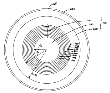
Referring to FIG. 2, photonic crystal fiber 120 includes a core 220 extending
along a
2s waveguide axis and a dielectric confinement region 210 (e.g., a multilayer
cladding)
surrounding the core. Confinement region 210 is surrounded by a support layer
250, which
provides mechanical support for the confinement.region. Optionally, support
layer 250 is
surrounded by sheath 165. A space 265 exists between sheath 165 and fiber 120.
As
discussed previously, a liquid or gas can be forced through the space between
the sheath and
30 the cladding to cool the fiber during operation.
1o
CA 02504951 2005-05-02
WO 2004/049042 PCT/US2003/037723
In the embodiment of FIG. 2, confinement region 210 is shown to include
alternating
layers 230 and 240 of dielectric materials having different refractive
indices. One set of
layers, e.g., layers 240, define a high-index set of layers having an index nH
and a thickness
dH, and the other set of layers, e.g., layers 230, define a low-index set of
layers having an
index n, and a thickness d~, where n,-, > n~ (e.g., nH - n~ can be greater
than or equal to or
greater than 0.01, 0.05, 0.1, 0.2, 0.5 or more). For convenience, only a few
of the dielectric
confinement layers are shown in FIG. 1. In practice, confinement region 210
may include
many more layers (e.g., more than about 15 layers, 20 layers, 30 layers, 40
layers, 50 layers,
such as 80 or more layers).
Although not illustrated in FIG. 2, fiber 120 may include one or more
additional
layers between the confinement region and the core. For example, the fiber may
include one
or more layers selected to tailor the dispersion characteristics'of the fiber.
Examples of such
fibers are described in U.S. Patent Application Serial No. 10/057,440,
entitled "PHOTONIC
CRYSTAL OPTICAL WAVEGUIDES HAVING TAILORED DISPERSION PROFILES,"
~ 5 filed January 25, 2002, and having Pub. No. US-2002-0176676-A1, the entire
contents of
which are hereby incorporated by reference.
Layers 240 include a material having a high.refractive index, such as a
chalcogenide
glass. The high index material in layers 240 can be rheologically compatible
with the
material forming layers 230. The material in each of layers 240 can be the
same or different.
2o Layers 230 include a material having a refractive index lower than the high
index material of
adjacent layers 240, and can include a second chalcogenide glass or an oxide
glass. In
embodiments where layers 230 and 240 both include chalcogenide glasses, the
glasses are
usually different. The material in each of layers 230 can be the same or
different. Examples
of high and low index materials are described below.
25 In the present embodiment, core 220 is hollow. Optionally, the hollow core
can be
filled with a fluid, such as a gas (e.g., air, nitrogen, and/or a noble gas)
or liquid (e.g., an
isotropic liquid or a liquid crystal). Alternatively., core 220 can include
any material or
combination of materials that are rheologically compatible with the materials
forming
confinement region 210. In certain embodiments, core 220 can include one or
more dopant
3o materials, such as those described in U.S. Patent Application Serial No.
10/121,452, entitled
"HIGH INDEX-CONTRAST FIBER WAVEGUIDES AND APPLICATIONS," filed April
11
CA 02504951 2005-05-02
WO 2004/049042 PCT/US2003/037723
12, 2002 and now published under Pub. No. US-2003-0044158-A1, the entire
contents of
which are hereby incorporated .by reference.
Photonic crystal fiber 120 has a circular cross-section, with core 220 having
a circular
cross-section and region 210 (and layers therein) having an annular cross-
section. In other
embodiments, however, the waveguide and its constituent regions may have
different
geometric cross-section such as a rectangular or a hexagonal cross-section.
Furthermore, as
mentioned below, core and confinement regions 220 and 210 may include multiple
dielectric
materials having different refractive indices. In such cases, we may refer to
an "average
refractive index" of a given region, which refers to the sum of the weighted
indices for the
constituents of the region, where each index is weighted by the fractional
area in the region
of its constituent. The boundary between region z20 and 210, however, is
defined by a
change in index. The change may be caused by the interface of two different
dielectric
materials or by different dopant concentrations in the same dielectric
material (e.g., different
dopant concentrations in silica).
~ 5 Dielectric confinement region 210 guides EM radiation in a first range of
wavelengths to propagate in dielectric core 220 along the waveguide axis. The
confinement
mechanism is based on a photonic crystal structure in region 210 that forms a
bandgap
including the first range of wavelengths. .Because the confinement mechanism
is not index-
guiding, it is not necessary for the core to have a higher index than that of
the portion of the
2o confinement region immediately adjacent the core. To the contrary, core 220
may have a
lower average index than that of confinement region 210. For example, core 220
may be air,
some other gas, such as nitrogen, or substantially evacuated. In such a case,
EM radiation
guided in the core will have much smaller losses and much smaller nonlinear
interactions
than EM radiation guided in a silica core, reflecting the smaller absorption
and nonlinear
25 interaction constants of many gases relative to silica or other such solid
material. In
additional embodiments, for example, core 220 may include a porous dielectric
material to
provide some structural support for the surrounding confinement region while
still defining a
core that is largely air. Accordingly, core 220 need not have a uniform index
profile.
The alternating layers 230 and 240 of confinement region 210 form what is
known as
3o a Bragg fiber. The alternating layers are analogous to the alternating
layers of a planar
dielectric stack reflector (which is also known as a Bragg mirror). The
annular layers of
12
CA 02504951 2005-05-02
WO 2004/049042 PCT/US2003/037723
confinement region 210 and the alternating planar layers of a dielectric stack
reflector are
both examples of a photonic crystal structure. Photonic crystal structures are
described
generally in Photonic Crystals by John D. Joannopoulos et al: (Princeton
University Press,
Princeton NJ, 1995).
As used herein, a photonic crystal is a dielectric structure with a refractive
index
modulation that produces a photonic bandgap in the photonic crystal. A
photonic bandgap,
as used herein, is a range of wavelengths (or inversely, frequencies) in which
there are no
accessible extended (i.e., propagating, non-localized) states in the
dielectric structure.
Typically the structure is a periodic dielectric structure, but it may also
include, e.g., more
complex "quasi-crystals." The bandgap can be used to confine, guide, and/or
localize light
by combining the photonic crystal with "defect" regions that deviate from the
bandgap
structure. Moreover, there are accessible extended states for wavelengths both
below and
above the gap, allowing light to be confined even in lower-index regions (in
contrast to
index-guided TIR structures, such as those described above). The term
"accessible" states
~ 5 means those states with which coupling is not already forbidden by some
symmetry or
conservation. law of the system. For example, in two-dimensional systems,
polarization is
conserved, so only states of a similar polarization need to be excluded from
the bandgap. In
a waveguide with uniform cross-section (such as a typical fiber), the
wavevector ~i is
conserved, so only states with a given ,l3 need to be excluded from the
bandgap to support
2o photonic crystal guided modes. Moreover, in a waveguide with cylindrical
symmetry, the
"angular momentum" index m is conserved, so only modes with the same m need to
be
excluded from the bandgap. In short, for high-symmetry systems the
requirements for
photonic bandgaps are considerably relaxed compared to "complete" bandgaps in
which all
states, regardless of symmetry, are excluded.
25 Accordingly, the dielectric stack reflector is highly reflective in the
photonic bandgap
because EM radiation cannot propagate through the stack. Similarly, the
annular layers in
confinement region 210 provide confinement because they are highly reflective
for incident
rays in the bandgap. Strictly speaking, a photonic crystal is only completely
reflective in the
bandgap when the index modulation in the photonic crystal has an infinite
extent. Otherwise,
3o incident radiation can "tunnel" through the photonic crystal via an
evanescent mode that
couples propagating modes on either side of the photonic crystal. In practice,
however, the
'13
CA 02504951 2005-05-02
WO 2004/049042 PCT/US2003/037723
rate of such tunneling decreases exponentially with photonic crystal thickness
(e.g., the
number of alternating layers). ~It also decreases with the magnitude of the
index-contrast in
the confinement region.
Furthermore, a photonic bandgap may extend over only a relatively small region
of
s propagation vectors. For example, a dielectric stack may be highly
reflective for a normally
incident ray and yet only partially reflective for an obliquely incident ray.
A "complete
photonic bandgap" is a bandgap that extends over all possible wavevectors and
all
polarizations. Generally, a complete photonic bandgap is only associated with
a photonic
crystal having index modulations along three dimensions. However, in the
context of EM
radiation incident on a photonic crystal from an adjacent dielectric material,
we can also
define an "omnidirectional photonic bandgap," which is a photonic bandgap for
all possible
wavevectors and polarizations for which the adjacent dielectric material
supports propagating
EM modes. Equivalently, an omnidirectional photonic bandgap can be defined as
a photonic
band gap for all EM modes above the light line, wherein the light line defines
the lowest
15 frequency propagating mode supported by the material adjacent the photonic
crystal. For
example, in air the light line is approximately given by r.~ = chi, where w is
the angular
frequency of the radiation, ~ is, the wavevector, and c is the speed of light.
A description of
an omnidirectional planar reflector is disclosed in U.S. Patent 6,130,780, the
contents of
which are incorporated herein by reference. Furthermore, the use of
alternating dielectric
20 layers to provide omnidirectional reflection (in a planar limit) for a
cylindrical waveguide
geometry is disclosed in U.S. Patent No. 6,463,200, entitled "OMNIDIRECTIONAL
MULTILAYER DEVICE FOR ENHANCED OPTICAL WAVEGUID1NG," to Yoel Fink et
al., the contents of which are incorporated herein by reference.
When alternating layers 230 and 240 in confinement region 210 give rise to an
25 omnidirectional bandgap with respect to core 220, the guided modes are
strongly confined
because, in principle, any EM radiation incident on the confinement region
from the core is
completely reflected. However, such complete reflection only occurs when there
are an
infinite number of layers. For a finite number of layers (e.g., about 20
layers), an
omnidirectional photonic bandgap may correspond to a reflection in a planar
geometry of at
30 least 95 % for all angles of incidence ranging from 0° to 80°
and for all polarizations of EM
radiation having frequency in the omnidirectional ~bandgap. Furthermore, even
when
14
CA 02504951 2005-05-02
WO 2004/049042 PCT/US2003/037723
photonic crystal fiber 120 has a confinement region with a bandgap that is not
omnidirectional, it may still support a strongly guided mode, e.g., a mode
with radiation
losses of less than 0.1 dB/km for a range of frequencies in the bandgap.
Generally, whether
or not the bandgap is omnidirectional will depend on the size of the bandgap
produced by the
alternating layer (which generally scales with index-contrast of the two
layers) and the
lowest-index constituent of the photonic crystal.
In additional embodiments, the dielectric confinement region may include
photonic
crystal structures different from a multilayer Bragg configuration. For
example, rather than
the Bragg configuration, which is an example of a one-dimensionally periodic
photonic
crystal (in the planar limit), the confinement region may be selected to form,
for example, a
two-dimensionally periodic photonic crystal (in the planar limit), such as an
index
modulation corresponding to a~honeycomb structure. See, for example, R.F.
Cregan et al.,
Science 285, p. 1537-1539, 1999. Furthermore, even ima Bragg-like
configuration, the high-
index layers may vary in index and thickness, and/or the low-index layers may
vary in index
~ 5 and thickness. The confinement region may also include a periodic
structure including more
than two layers per period (e.g., three or more layers per period). Moreover,
the refractive
index modulation may vary continuously or discontinuously as a function of
fiber radius
within the confinement region. In general, the confinement region may be based
on any
index modulation that creates a photonic bandgap.
2o In the present embodiment,. multilayer structure 210 forms a Bragg
reflector because
it has a periodic index variation with respect to the radial axis. A suitable
index variation is
an approximate quarter-wave condition. It is well-known that; for normal
incidence, a
maximum band gap is obtained for a "quarter-wave" stack in which each layer
has equal
optical thickness ~,/4, or equivalently dH l d~ = n~ l nH , where d and n
refer to the thickness
25 and index, respectively, of the high-index and low-index layers. These
correspond to layers
240 and 230, respectively. Normal incidence corresponds, to (3 = 0. For a
cylindrical
waveguide, the desired modes typically lie near the light line ~ = c~3 (in the
large core radius
limit, the lowest-order modes are essentially plane waves propagating along z-
axis, i.e., the
waveguide axis). In this case, the quarter-wave condition becomes:
CA 02504951 2005-05-02
WO 2004/049042 PCT/US2003/037723
dH - ncz _ 1
do _ nHZ _l.
Strictly speaking, this equation may not be exactly optimal because the
quarter-wave
condition is modified by the cylindrical geometry; which may require the
optical thickness of
each layer to vary smoothly with its radial coordinate. Nonetheless, we find
that this
equation provides an excellent.guideline for optimizing many desirable
properties, especially
for core radii larger than the mid-bandgap wavelength. .
Some embodiments of photonic crystal fibers are described in U.S.Patent
Application
Serial No. 10/057,258, entitled "LOW-LOSS PHOTONIC CRYSTAL FIBER HAVING
LARGE CORE RADIUS," to Steven G. Johnson. et al., filed January 25, 2002 and
published
under Pub. No. US-2002-0164137-A1, the entire contents of which are hereby
incorporated
by reference.
The radius of core 220 can vary depending on the end-use application of fiber
120.
The core radius can depend on the wavelength or wavelength range of the energy
to be
guided by the fiber, and on whether the fiber is a single or,multimode fiber.
For example,
~5 where the fiber is a single mode fiber for guiding visible wavelengths
(e.g., between about
400 nm and 800 nm) the core radius can be in the sub-micron to several micron
range (e.g.,
from about 0.5 ~m to 5 pm). However, where the fiber is a multimode fiber for
guiding IR
wavelengths (e.g., from about 2 pm to 15 pm, such as 10.6 pm), the core radius
can be in the
tens to thousands of microns range (e.g., from about 10 pm to 2,000 Vim, such
as 500 ~m to
20 1,000 pm). The core radius can be greater than about 57~ (e.g:, more than
about 10~,, 207,
50~,, 100,), where 7~ is the wavelength of the guided energy.
Two mechanisms by which energy can be lost from a guided signal in a photonic
crystal fiber are by absorption loss and radiation loss. Absorption loss
refers to loss due to
material absorption. Radiation loss refers to energy that leaks from the fiber
due to imperfect
25 confinement. Both modes of loss can be studied theoretically, for example,
using transfer
matrix methods and perturbation theory. A discussion of transfer matrix
methods can be
found in an article by P. Yeh et al., J. Opt. Soc. Am., 68', p: 1196 (1978). A
discussion of
perturbation theory can found in an article by M. Skorobogatiy et al., Optics
Express, 10, p.
1227 (2002). Particularly, transfer matrix code finds propagation constants /3
for the "leaky"
16
CA 02504951 2005-05-02
WO 2004/049042 PCT/US2003/037723
modes resonant in a photonic crystal fiber structure. Imaginary parts of ~'s
define the modal
radiation loss, thus Lossr~~int,o" ~ Im(~. Loss due to material absorption is
calculated using
perturbation theory expansions, and in terms of the modal field overlap
integral it can be
determined from
LOSSnbsorprion ~ 2~~ ~rdr(aE~E~ ) ,
0
where ~ is the radiation frequency, r is the fiber radius, a is bulk
absorption of the material,
and Ea is an electric field vector.
Based on theoretical and/or empirical investigations, photonic crystal fibers,
such as
fiber 120, can be designed to minimize one or both mode of loss. Guided modes
can be
classified as one of three types: pure transverse electric (TE); pure
transverse magnetic (TM);
and mixed modes. Loss often depends on the type of mode. For example, TE modes
can
exhibit lower radiation and absorption losses than TM/mixed modes.
Accordingly, the fiber
can be optimized for guiding a mode that experiences low radiation and/or
absorption loss.
Alternatively, or additionally, the fiber can be optimized for a mode that is
well matched to
~ 5 the mode of laser 110. For example, the fiber can be optimized for guiding
the HEM 1 (mixed)
mode, which is well matched to the TEMoo mode of a laser. Being "well matched"
refers to
efficient coupling between the mode of the laser and the guided mode of the
fiber.
Radiation loss can be reduced by adding layers to the confinement region of
fiber
120, increasing the index contrast between the high and low index layers,
increasing the core
2o radius and/or lowering the intrinsic absorption,losses of the first few
layers by selecting
materials with low absorption at the guided wavelengths. For example, at
wavelengths of
about 3 microns, chalcogenide glasses exhibit an absorption coefficient of
about 4 dB/m
compared to many polymers which have an absorption coefficient of about 105
dB/m in that
wavelength range. Similarly, at 10.6 microns, chalcogenide glasses have an
absorption
25 coefficient of about 10 dB/m compared to 105 dB/m for many polymers. Thus,
using
chalcogenide glasses instead of polymers can reduce losses in some cases.
However,
polymers, like oxide glasses, can provide lower index materials than
chalcogenide glasses.
As an example, consider a photonic crystal fiber having a core radius R; = 500
pm,
the confinement region materials have indices of n~ = 2.3 and n,, = 2.7, with
a bi-layer
3o thickness, d = 2.3 pm. The corresponding thickness of the low index and
high index layers
m
CA 02504951 2005-05-02
WO 2004/049042 PCT/US2003/037723
are 1.3 ~m and 1.0 Vim, respectively. For the purposes of this example, the
intrinsic bulk
absorption loss of high/low index materials is taken to be TO dB/m. The
support layer (R~ _
1500 Vim) is assumed to have absorption loss of l OSdB/m, typical of polymers.
The
confinement region has 55 layers, thus R,n = 563 Vim.
At ~, = 10.6 Vim, a theoretical model indicates that these structural
parameters define a
fiber radiation loss of 24 dB/km (with a radiation loss decreasing by about an
order of
magnitude with every 30 layers added to the confinement region), and a
material absorption
loss in the confinement region of 0.23 dB/km. Adding 60 more layers to the
confinement
region reduces radiation loss, which then becomes comparable to the material
absorption loss
in the mirror. These results are summarized in FIG 3A and FIG 3B, which
respectively
show the dependence of the radiation and absorption losses on the operating
wavelength.
In contrast, consider a fiber having a similar structure; except where the low
index
and high index materials have refractive indices of n~ = 1.5 and nh = 2.8,
with a bi-layer
thickness of d=2.82 pm (the bi-layer refers to a high index and low index
layer pair). These
~5 refractive index values are representative of a polymer low index material
and a chalcogenide
glass high index material. The corresponding layer thicknesses are 1.97 pm and
0.84 ~m for
the low and high index layers, respectively. The intrinsic bulk absorption
loss of high index
material is 10 dB/m. The support layer (R~ = 1500 Vim) and low index material
are assumed
to have absorption loss of l OSdB/m, typical of polymers. In this example, the
confinement
2o region is assumed to have 35 layers (17.5 bi-layers), thus R", = 549 pm.
At 7~=10.6 Vim, these structural parameters define a fiber radiation loss of
1.09 dB/km
(with a radiation loss decreasing by an order of magnitude with every 4 bi-
layers added), and
a material absorption loss, in the mirror, of 320dB/km, where power
dissipation loss will be
dominated by material absorption in the first few polymer layers of the
confinement region.
25 Accordingly, in some embodiments, the low index material can be selected to
have
low absorption loss in the first few layers of the confinement region, and
higher relative
absorption loss in outer layers.' The index contrast can be higher in the
outer layers compared
the inner layers. For example, the confinement region can have low index
layers that include
a chalcogenide glass in layers close to the core, but include a polymer or
oxide glass in layers
3o further from the core. The high index layers can include a chalcogenide
glass throughout.
18
CA 02504951 2005-05-02
WO 2004/049042 PCT/US2003/037723
As discussed previously, materials can be selected for the confinement region
to
provide advantageous optical properties (e.g., low absorption with appropriate
indices of
refraction at the guided wavelength(s)). However, the materials should also be
compatible
with the processes used to manufacture the fiber. In some embodiments, the
high and low
index materials (e.g., the first and second chalcogenide glasses) should
preferably be
compatible for co-drawing. Criteria for co-drawing compatibility are provided
in
aforementioned U.S. Patent Application Serial No. 10/121,452, entitled "HIGH
INDEX-
CONTRAST FIBER WAVEGUIDES AND APPLICATIONS." In addition, the high and
low index materials should preferably be sufficiently stable with respect to
crystallization,
phase separation, chemical attack and unwanted reactions for the conditions
(e.g.,
environmental conditions such as temperature, humidity, and ambient gas
environment)
under which the fiber is formed, deployed, and used.
As mentioned in the foregoing description of fiber 120, layers 240 and 230 can
include a first and second chalcogenide glass, respectively (e.g., glasses
containing a
~ 5 chalcogen element, such as sulphur, selenium, and/or tellurium). In
addition to a chalcogen
element, chalcogenide glasses may include one or more of the following
elements: boron,
aluminum, silicon, phosphorus; sulfur, galliurri, germanium, arsenic, indium,
tin, antimony,
thallium, lead, bismuth, cadmium, lanthanum and the halides (fluorine,
chlorine, bromide,
iodine).
2o Chalcogenide glasses can be binary or ternary glasses, e.g., As-S, As-Se,
Ge-S, Ge-
Se, As-Te, Sb-Se, As-S-Se, S-Se-Te, As-Se-Te, As-S-Te, Ge-S-Te, Ge-Se-Te, Ge-S-
Se, As-
Ge-Se, As-Ge-Te, As-Se-Pb, As-S-Tl, As-Se-Tl, As-Te-Tl, As-Se-Ga, Ga-La-S, Ge-
Sb-Se or
complex, mufti-component glasses based on these elements such as As-Ga-Ge-S,
Pb-Ga-Ge-
S, etc. The ratio of each element in a chalcogenide glass can be varied.
25 The amount of the first chalcogenide glass in the high index material can
vary.
Typically, the high index material includes at least about 5.0% by weight of
the first
chalcogenide glass (e.g., at least 70%, 80%, 90%, 95%,' 98%, 99%). The high
index material
can be substantially exclusively chalcogenide glass (i.e.,.about 100%
chalcogenide glass). In
some embodiments, in addition to the first chalcogenide glasses, the high
index material can
3o include one or more additional chalcogenide glasses, heavy metal oxide
glasses, amorphous
alloys, or combinations thereof.
19
CA 02504951 2005-05-02
WO 2004/049042 PCT/US2003/037723
In some embodiments, 'the high.index material is a chalcogenide glass
including As
and Se. For example, the high index material can include As2Se3. As2Se3 has a
glass
transition temperature (Tg) of about 180°C and a thermal expansion
coefficient (TEC) of
about 24 x 10-6/°C. At 10.6 Vim, As2Se3 has a refractive index of
2.7775, as measured by
Hartouni and coworkers and described in Proc. SPIE, SOS, 11 (1984), and an
absorption
coefficient, a, of 5.8 dB/m, as measured by Voigt and Linke and described in
"Physics and
Applications of Non-Crystalline Semiconductors in Optoelectronics," Ed. A.
Andriesh and
M. Bertolotti, NATO ASI Series, 3. High Technology, Vol. 36, p. 155 (1996).
Both of these
references are hereby incorporated by reference in their entirety.
The first chalcogenide glass can include As2Se3 and one or more other
elements.
Examples of other elements that can be included are In, Sn, Sb, Te, I, Tl, Pb,
and/or Bi. The
index of the first chalcogenide glass can be greater than.the refractive index
of As2Se3. For
example, chalcogenide glasses including Sb and/or Te in addition to As2Se3 can
increase the
refractive index of the chalcogenide glass above the refractive index of
As2Se3. The
~ 5 refractive index of the first chalcogenide glass in .these embodiments can
be greater than
about 2.8 (e.g., more than 2.9, such as about 3.0 or more).
Some elements that can be added to As2Se3 to increase the refractive index of
the. first
chalcogenide glass can change the thermomechanical properties of the first
chalcogenide
glass from the thermomechanical properties of AsZSe3. The thermomechanical
properties
2o include phase transition temperatures, such as Tg,, and other parameters
such as the glass's
TEC. For example, iodine may increase the refractive index of the first
chalcogenide glass,
but can reduce Tg. In such cases, one or more additional compounds may be
added to the
first chalcogenide glass to mitigate the effects of the index-raising element
on the glasses
thermomechanical properties. On example of an element that can reduce such
25 thermomechanical effects is Ge. Iri embodiments; the second chalcogenide
glass can have a
Tg of more than about 180°C (e.g., about 200°C,
220°C, 250°C or more).
The amount of additional compounds added to As2Se3 in the first chalcogenide
glass
can vary. Typically, the amount of various elements in the first chalcogenide
glass is
determined empirically according to the specifics of the photonic crystal
fiber. For example,
3o where the fiber design requires the first chalcogenide glass to have
specific refractive index,
an amount of an index-raising element sufficient to provide the desired index
is added.
CA 02504951 2005-05-02
WO 2004/049042 PCT/US2003/037723
Preferably, the amount of any index-raising element included will be
sufficiently small to not
substantially affect the stability of the glass (e.g., to prevent phase
separation of the glass
components). In some embodiments, the amount of AszSe3 in the first
chalcogenide glass
can be more than about 80% molar (e.g., more than about 90%, 95%, 99%) and the
amount
of one or more additional elements can be less than about 20% molar (e.g.,
less than about
10%, 5%, I %).
The amount of the second chalcogenide glass in the low index material can
vary.
Typically, the low index material includes at least about SO% by weight of the
second
chalcogenide glass (e.g., at least 70%, 80%, 90%, 95%, 98%, 99%). The low
index material
can be substantially exclusively chalcogenide glass (i.e., about 100%
chalcogenide glass). In
some embodiments, in addition to the second chalcogenide glasses, the high
index material
can include one or more additional chalcogenide glasses, heavy metal oxide
glasses,
amorphous alloys, or combinations thereof.
In some embodiments, the low index material is a chalcogenide glass including
As
~5 and Se. For example, the high index material can include As2Se3.
The second chalcogenide. glass can include AsZSe3 and one or more other
elements.
Examples of other elements that can be included are B, F, Al; Si, P, S, and/or
Ge. In these
embodiments, the index of the second chalcogenide glass can be less than the
refractive
index of As2Se3. For example, chalcogenide glasses including P and/or S in
addition to
2o As2Se3 can reduce the refractive index of the chalcogenide glass below the
refractive index of
AsZSe3. The refractive index of the second chalcogenide glass in these
embodiments can be
less than about 2.7 (e.g., less than 2.5, such as about 2.0 or less).
Some elements that can be added to As2Se3 to reduce the refractive index of
the
second chalcogenide glass can change the thermomechanical properties of the
first
25 chalcogenide glass from the thermomechanical properties of AsZSe3. For
example, Si may
reduce the refractive index of the second chalcogenide glass, and can increase
Tg. In some
such cases, one or more additional compounds may be added to the second
chalcogenide
glass to mitigate the effects of the index-reducing element to ensure the low
index material is
compatible with the high index material. In embodiments, the second
chalcogenide glass can
3o have a Tg of more than about 180°C (e.g., about 200°C,
220°C, 250°C or more).
21
CA 02504951 2005-05-02
WO 2004/049042 PCT/US2003/037723
The amount of additional compounds added to As2Se3 in the second chalcogenide
glass can vary. Typically, the amount of various elements in the second
chalcogenide glass
is determined empirically according to the specifics of the photonic crystal
fiber. For
example, where the fiber design requires the second chalcogenide glass to have
specific
refractive index, an amount of an index-reducing element sufficient to provide
the desired
index is added. Preferably, the amount of any index-reducing elements included
will be
sufficiently small to not substantially affect the stability of the glass
(e.g., to prevent phase
separation of the glass components). In some embodiments, the amount of AsZSe3
in the
second chalcogenide glass can be more than about 80% molar (e.g., more than
about 90%,
95%, 99%) and the amount of one or more additional elements can be less than
about 20%
molar (e.g., less than about 109'0, 5%, 1.%).
In some embodiments, the second chalcogenide glass can include As2S3, GePS,
and/or ASPS. The composition of the second chalcogenide glass including AszS3,
GePS,
and/or ASPS can be manipulated to obtain a desired refractive index and/or
15 thermomechanical properties as described for AszSe3 above. .
The first and/or second,chalcogenide glasses can have relatively low loss at a
wavelength of interest compared to some non-chalcogenide glasses and/or some
polymers
(e.g., PES). For example, at 10.6 microns, the first and/or second
chalcogenide glasses can
have a loss co-efficient of less than about 1,000 dB/m. More preferably, the
first and/or
2o second chalcogenide glasses can have a loss coefficient of less than about
50 dB/m, such as
less than about 20 dB/m, 10 dB/m or less. In contrast, polymers such as PES
can have a loss
co-efficient of 10,000 dB/m or more.
In order for dielectric waveguides to function reliably at high power
densities, they
should have low defect densities. In photonic crystal fibers, such as those
described herein,
25 defects include delamination between layers, cracking, or other structural
defects, and
material defects, such as impurities. Selecting materials with matched
thermomechanical
properties can reduce the occurrence of defects. One way to form preforms of
these
materials with high purity is to use CVD.
In embodiments where CVD is used, the high and low index materials (e.g., the
first
3o and second chalcogenide glasses) should be compatible with this process. To
be compatible
22
CA 02504951 2005-05-02
WO 2004/049042 PCT/US2003/037723
with CVD, precursors for the compounds from which solid deposits can be formed
should be
available for forming the high and low index materials.
Referring to FIG 4, during the CVD process, a CVD system 500 is used to
deposit
layers of different materials on the inner surface of a deposition tube 501.
CVD system 500
s includes a gas source 510, a gas manifold 520, and a lathe 530 on which
deposition tube 501
is mounted. The material the system deposits in tube 501 forms in a chemical
reaction
between gases supplied to tube 501 by gas source 510 via manifold 520. System
500 also
includes a microwave source 550, which excites a plasma in the gas within the
tube, causing
the gases to react and deposit material on the tube surface, A furnace 540
heats tube 501 to a
1o desired temperature during the deposition process. System 500 also includes
tubes 570 that
transport gases from gas source 510 to manifold 520. Valves 580 modulate the
flow of gases
from gas source 510 to manifold 520. The gases mix inside manifold 520 before
being
transported to deposition tube 501 via a pipe 590. The deposition process is
controlled by an
electronic controller 560 (e.g., a system including a processor for executing
instructions, such
15 as a computer).
Referring also to FIG f, microwave source 550 includes a resonator enclosing a
segment of deposition tube 501. During operation, the resonator couples
microwave energy
from a waveguide into gas (e.g., vapor) within tube 501. Typically, this
energy has a
frequency in the range of about 1 to about 40 GHz. For example, the energy can
have a
2o frequency of about 5 to 15 GHz, such as about 12.5 GHz. The energy
generates a local non-
isothermal low-pressure plasma region 610 within the tube. Gas flowing through
the
deposition tube is deflected by plasma region 610 to the. space between plasma
region 610
and tube 501, as indicated by arrows 620 and 630. Gasses proximate to the
plasma react with
each other, forming a layer of material one the inner surface of tube 501
adjacent plasma 610.
25 Preferably, microwave energy is transferred without substantial energy loss
to the tube itself,
and microwave energy is coupled directly into.the activated plasma inside the
tube.
During operation, system 500 translates microwave source 550 back and forth
along
the axis of tube 501, exciting plasma in the portion of the tube, adjacent the
source. Each pass
of microwave source 500 relative to the tube results in a layer of material
being deposited
3o within the tube. The microwave source 550 can be translated as many times
as necessary to
provide the desired thickness of material with iri the tube.
23
CA 02504951 2005-05-02
WO 2004/049042 PCT/US2003/037723
Furnace 540 heats the tube surface to a temperature sufficient to ensure that
deposited
materials diffuse to form a consolidated layer. For this reason, the
temperature depends upon
the type of material being deposited. For many materials, the tube is heated
to a temperature
between about 80°C and 250°C, such as about 100°C. The
tube temperature is kept below a
temperature that would cause any substantial adverse reaction in the deposited
layer. For
example, chalcogenide glasses may oxidize at temperatures above 250°C -
300°C. Thus, for
these glasses, the tube surface is maintained below these temperatures. Lower
process
temperatures can also reduce mechanical stress in the deposited layers,
reducing the
possibility of fracture and/or delamination in the multilayer structure. The
tube surface
temperature may be varied between depositing layers of different materials
therein.
Controller 560 controls numerous parameters associated with the deposition
process
to provide a layer of material having the desired thickness and material
properties (e.g.,
composition, density, homogeneity and/or layer morphology). These parameters
include
surface temperature, gas pressure, gas composition, microwave energy, and
microwave
~ 5 frequency. The effects of the parameters on deposition rate and material
properties are
typically interrelated. For example, changes in gas pressure and/or gas
composition can
affect the deposition rate by providing more or less of one or more reactant
gases to the tube.
Variations in microwave energy and/or frequency can vary the deposition rate
by changing
the temperature of the tube surface.
2o Due to its shape, plasma region 610 is often referred to as a plasma
"ball." The shape
and size of the plasma ball is related to,the plasma mode excited by the
radiation and can be
affected by gas pressure, the shape of the cavity, the gas composition, and/or
the ionization
potential of the gas. For example, under otherwise equivalent conditions, the
size of a
plasma ball formed in nitrogen is typically smaller than a plasma ball formed
in argon.
25 Because the gas phase reaction of component gases occurs proximate to the
plasma ball, the
shape and size of the plasma ball can be selected to control the tube area
over which
deposition occurs. In many embodiments, where the deposition tube is
cylindrical, the Toy
plasma mode is desirable.
Initially, a first gas composition is used to produce a layer of a first
material. After
3o depositing the first material but prior to depositing the second material
the tube is purged of
residual reactive gases. Typically, the system flows an inert gas (i.e., inert
with respect to the
24
CA 02504951 2005-05-02
WO 2004/049042 PCT/US2003/037723
layer of material just deposited in the tube and with residual gases in the
tube) through the
tube for a time sufficient to purge substantially all of the first gas
composition from the tube.
Examples of inert gases include nitrogen and noble gases, such as argon. The
system can
monitor the composition of gas purged from the tube to establish when the
concentration of
the first gas composition in the, tube is sufficiently small to be negligible.
The first and second gas compositions include component gases that react upon
heating by the plasma to form the first and second materials, respectively.
The type and
relative concentration of component gases are selected based on the desired
composition of
the materials. In embodiments where either of the materials are a chalcogenide
glass, at least
one of the respective component gases includes a chalcogen element. In
embodiments where
either of the materials is an oxide glass; the respective gas composition
includes oxygen (e.g.,
as oxygen gas or the gas of an oxygen containing compound). In each gas
composition, one
or more of the components can be a halide (e.g., a chloride) gas or a hydride
gas. Examples
of chlorides include SiCl4, BC13, POCl3, PC13, GeCl4, SeClz, AsCl3, and SzCl2.
Examples of
~5 hydrides include HZSe, GeH4, HZS, HZTe, AsH3; and PH3. In some embodiments,
chlorides
may be preferred over hydrides, especially where hydrogen and/or oxygen can
contaminate
the deposited material. Such contamination may occur where decomposition of
the
component gas is incomplete and/or due to the presence of water and/or oxygen.
During the deposition of a Iayer of the first or second material, the relative
2o concentration of component gases can remain the same or vary. Where a
homogeneous layer
is desired, the relative concentration of component gases is substantially
constant. However,
where variations in composition are desired through the layer, the relative
concentration of
component gases can vary during deposition of the layer. For example, where a
refractive
index gradient through the layer is desired, the relative concentration of
component gases can
25 be varied during deposition of the layer.
The first and/or second gas compositions can also include a Garner gas, which
is inert
with respect to the other component gases. A carrier gas can be used to adjust
the pressure of
the first gas composition without affecting the relative concentration of the
component gases.
Carrier gases are selected based on. the composition of the component gases.
Examples of
3o carrier gases include nitrogen and noble gases,.such as argon, and mixtures
thereof.
CA 02504951 2005-05-02
WO 2004/049042 PCT/US2003/037723
The ratio of carrier gas to component (reactant) gases) in a gas composition
may
vary as desired. Typically, the ratio of Garner to component gases) is between
about 1:10
and 1:10- . The relative amount of component gases) to carrier gas can affect
the deposition
rate and the morphology of the deposited material.
In some embodiments, 'the first deposited layer may adversely react with a
compound
or element forming the subsequent layer while that element or compound is in
the form of a
gas. An adverse reaction introduces impurities into the preform, which can be
detrimental to
fiber performance. For example, where an oxide glass is being deposited onto a
layer of a
chalcogenide glass, gaseous oxygen can oxidize the chalcogenide glass. In such
instances, an
inert component gas containing the reactive element or compound can be chosen
for the gas
composition to reduce (e.g., mitigate) any adverse reaction between the gas
and the
previously deposited layer (or tube). An example of a gas that can be used to
provide oxygen
when depositing an oxide glass on a chalcogenide (or other oxidizable glass)
is nitrous oxide.
In some embodiments, the relative concentration of the reactive gas (e.g.,
oxygen) can be
~5 increased once a thin layer of material (e.g., oxide glass) has been
deposited on the previous
layer.
Material may be deposited at relatively high rates. For example, the
deposition rate
may be about 1 pm/min or more (e.g., more than about S p.m/min, 8 pm/min, 10
pm/min).
In general, tube 501 can be formed from any material. Where the tube forms
part of
2o the final drawn fiber, the tube should be formed from a material that can
be co-drawn with
material deposited within the tube. In some embodiments, tube 501 is formed
from a glass or
a polymer. Examples of suitable glasses include silica-based glasses. Examples
of suitable
polymers include polysulfones, fluoropolymers (e.g., Teflon~), polyethylene
and their
derivatives.
25 Although microwave radiation is used to excite plasma in system 100, other
forms of
EM radiation can also be used.' For example, radio frequency radiation (e.g.,
with
frequencies less than about 109 Hz) can be used to excite plasma in the tube.
Furthermore, in
some embodiments, plasma can be excited thermally alternatively or
additionally to using
EM radiation.
3o To make a preform for a photonic crystal fiber, additional layers of
material can be
deposited on the layer of the second material. 'In some embodiments, the
sequential
26
CA 02504951 2005-05-02
WO 2004/049042 PCT/US2003/037723
deposition of layers of the first and second materials is repeated multiple
times (e.g., twice,
three time, four times, or more). Alternatively, the composition of, e.g., a
third layer may
differ from the composition of the first layer. For example, to make a preform
for a low loss
photonic crystal fiber, materials with high index contrast (e.g:, layers of a
chalcogenide glass
and an oxide glass) can be deposited initially, followed by layers of
materials with low
absorption (e.g., two different chalcogenide glasses). In some embodiments,
many layers can
be deposited (e.g., more than about 10 layers, such as 20 or more layers).
The thickness of each layer may vary as desired. Generally, the deposited
layer
thickness will depend on the desired structure of the waveguide and draw ratio
to be used in
subsequent fiber drawing. The' thickness of alternating layers may be the same
or different.
In some embodiments, layers are formed that have the same optical thickness.
Deposited
layer thickness is typically between about 0.1 nm and 500 pm.
Although the CVD methods described herein are with reference to photonic
crystal
fibers, they can also be used to make other types of waveguides (e.g., TIR
optical fibers).
15 Referring to FIG. 6, in some embodiments, system 100 may be modified to
simultaneously provide output energy from laser 110 at multiple locations.
Modified system
700 includes a number of couplers 710, which couple energy guided in waveguide
120 into
other waveguides 720. Each waveguide 720 can deliver laser energy to a
different location
remote from laser 110. Waveguides 720 can be the same or different as
waveguide 120. For
20 example, waveguides 720 can be photonic crystal fibers or some other type
of waveguide
(e.g., TIR fiber). The intensity of laser energy coupled into each waveguide
720 can be the
same or different. Where each waveguide's output is used in similar
applications, the
intensity delivered by each waveguide can be the same. However, where
applications are
different, the delivered intensity can vary accordingly.
25 It will be understood that various modifications to the foregoing
embodiments may be
made without departing from the spirit and scope of the invention.
Accordingly, other
embodiments are within the scope of the following claims.
27