Note: Descriptions are shown in the official language in which they were submitted.
CA 02505189 2005-05-05
WO 2004/049559 PCT/US2003/037499
1
SYSTEMS AND METHODS OF DYNAMIC BIAS SWTITCHING FOR RADIO
FREQUENCY POWER AMPLIFIERS
BACKGROUND OF THE INVENTION
[0001] The present invention relates to power amplifiers,
and more particularly to power amplifier systems in which
multiple signals are simultaneously transmitted at varying
power levels.
[0002] In electronic communication systems, it is often
necessary that groups of information signals be amplified
and transmitted simultaneously. For example, a cellular
radio base station transmitter typically transmits signals
to many active receiving mobile stations within a single
geographic cell. The signals typically appear at multiple
predetermined frequencies in such mufti-carrier signals.
Similarly, a satellite communications transponder amplifies
and transmits large number of information signals destined
for various participating remote stations. Because such
systems customarily employ a frequency division multiple
access (FDMA) scheme, in which information signals are
modulated on signal carriers occupying several frequency
channels within an allocated frequency band, care must be
taken to avoid inter-channel interference which may corrupt
signal transmissions.
[0003] One possible source of such cross-channel
interference is known as intermodulation distortion (IMD),
which may result when two or more signals of different
frequencies are mixed. For example, if two carriers of
different frequencies are amplified using a non-linear
CA 02505189 2005-05-05
WO 2004/049559 PCT/US2003/037499
2
amplifier, spurious outputs occur at the sum and difference
of integer multiples of the original carrier frequencies.
[0004] Third order intermodulation products resulting
from two relatively strong signals may disrupt transmission
of a third relatively weak signal being transmitted on a
carrier having a frequency equal to the frequency of the
intermodulation product. It is desirable to reduce this
distortion.
[0005] Base station power amplifier systems exhibiting a
high degree of linearity can be desirable since such
amplifiers can help minimize the out-of-band emissions and
allow for frequency reuse schemes. Amplifier systems are
made up of power amplifiers (or "gain blocks") to provide
more gain than possible with a single gain block.
[0006] Various solutions have been proposed for improving
linearity and reducing inter-channel effects in multi-
carrier amplifier systems. One such solution is the feed-
forward amplifier system. To further improve linearity in a
feed forward amplifier system predistorters may be added in
front of individual power amplifiers (gain blocks), or the
bias applied to gain blocks may be controlled.
[0007] In the feed-forward amplifier system two loops can
be used to cancel distortion. In a first loop, a portion of
the signals at the input to the amplifier are fed forward
and, following suitable amplitude and phase adjustment, are
subtracted from the amplifier output to generate an error
signal. The error signal is proportional to distortion
components of the output. The first loop that generates the
error signal is known as the signal-cancellation loop. The
error signal is then amplified, phase-adjusted and
CA 02505189 2005-05-05
WO 2004/049559 PCT/US2003/037499
3
subtracted from the amplifier output to give a corrected
signal output with reduced distortion effects. This portion
of the circuit is known as the error-cancellation loop.
[0008] Nonlinearity can be tolerated in a feed forward
amplifier system if the input signal to the amplifier has a
constant envelope. However, problems can arise when the
input signal has a large peak-to-peak average or signal
envelope.
[0009] In some recent digital modulation schemes with
improved bandwidth efficiency, information is embedded only
in a carrier phase. Nevertheless, the input signal is
typically characterized by a relatively large amplitude
variation or "signal envelope", and on average the signal
amplitude remains considerably lower than the frequent
signal peaks. To help control amplitude distortion and out
of band emissions, it is desirable for power amplifiers to
be capable of handling these frequent signal' peaks and
remain somewhat efficient in their power consumption. A way
to boost an amplifier's ability to faithfully reproduce
large dynamic range signals and maintain a degree of
efficiency is to switch in a greater power supply voltage
when it is needed. The power amplifier is required to
switch between these peaks. However, in the prior art
switch losses tend to negate the benefits of switching.
[0010] Conventional approaches have utilized continuous
tracking of the signal envelope. However, such approaches
can be inefficient and result in significant power losses,
particularly when the input signal is characterized by a
large average to peak ratio.
CA 02505189 2005-05-05
WO 2004/049559 PCT/US2003/037499
4
[0011] Accordingly, there is a need for controlling the
bias supply to help reduce intermodulation distortion in a
feed forward amplifier system that amplifies input signals
that vary considerably in amplitude. It is also desirable
to efficiently utilize the power applied to the amplifier
such that excessive power is not consumed, and that the
amplifier provides a linearity similar to that of an
amplifier biased for linear operation. For example, an
amplifier that is heavily biased class A or AB.
SUMMARY OF THE INVENTION
[0012] An aspect of the present invention provides a
method for linear amplification of an envelope of a
multicarrier input signal in a power amplifier that includes
an amplifier, comprising: determining the RF (Radio
Frequency) signal envelope; and switching a power supply
input to the amplifier between a first voltage level and a
second voltage level based on the RF signal envelope.
[0013] Another aspect of the present invention provides a
dynamic bias switching circuit, comprising means for
switching between a first signal level and a second signal
level based on a signal envelope of an input RF signal to an
amplifier. For example in an embodiment the first RF signal
envelope level is associated with a first power supply
level, or first bias level, and the second RF signal
envelope level is a second power supply level, or a second
bias level.
[0014] Another aspect of the present invention provides a
dynamic bias switching circuit adapted to provide a first
signal level and a second signal level, comprising an input
CA 02505189 2005-05-05
WO 2004/049559 PCT/US2003/037499
for a multicarrier input signal having a signal envelope;
means for determining the signal envelope; and means for
switching between the first signal level and the second
signal level based on the signal envelope.
5 [0015] Another aspect of the present invention provides a
power amplifier, comprising an amplifier that receives a
multicarrier input signal; and a dynamic bias switch unit
having an input coupled to the amplifier input signal and an
output coupled to the amplifier power supply, wherein the
l0 dynamic bias switch unit is adapted to switch a power supply
level applied to the amplifier between a first power supply
level and a second power supply level.
BRIEF DESCRIPTION OF DRAGTINGS
[0016] The following discussion may be best understood
with reference to the various views of the drawings,
described in summary below, which form a part of this
disclosure.
FIG. 1 is a block diagram of a conventional feed-
forward amplifier system;
FIG. 2 is a feed-forward power amplifier system having
dynamic bias switching;
FIG. 3 illustrates a block diagram of an amplifier from
the feed-forward power amplifier system having a dynamic
bias switch;
FIG. 4 is a time domain graph of an envelope of an RF
signal level that is applied to the amplifier;
FIG. 5 is a time domain graph showing how.the dynamic
bias switch switches the amplifier to a higher supply
voltage (VH) from a lower supply voltage (VL) when a
CA 02505189 2005-05-05
WO 2004/049559 PCT/US2003/037499
6
threshold voltage (VT) has been exceeded by the RF input
signal (VIN) applied to the input of the dynamic bias
switch;
FIG. 6 is a block diagram of an embodiment of a dynamic
bias switch;
FIG. 7 is a block diagram of an embodiment of the
extraction unit of the dynamic bias switch;
FIG. 8 is a block diagram of an embodiment of the
switch block of the dynamic bias switch;
FIG. 9 is a schematic of an embodiment of the dynamic
bias switch;
FIG. 10 is a flow diagram showing a method for linear
amplification of a multicarrier signal in a feed-forward
power amplifier system, by switching between amplifier power
supplies based upon input signal level;
FIG. 11 illustrates a block diagram of an amplifier and
digital predistorter combination including a dynamic bias
switch; and
FIG. 12 illustrates a block diagram of an amplifier and
predistorter combination including a dynamic bias switch;
FIG. 13 illustrates a block diagram of an amplifier
including a dynamic bias switch with a delay element
disposed in front of the amplifier.
DETAILED DESCRIPTION
[0017] The present invention is now described more fully
with reference to the accompanying drawings, in which
embodiments of the invention are shown. This invention may,
however, be embodied in many different forms and should not
be construed as limited to the embodiments set forth herein;
CA 02505189 2005-05-05
WO 2004/049559 PCT/US2003/037499
7
rather, these embodiments are provided so that this
disclosure will be thorough and complete, and will fully
convey the scope of the invention to those skilled in the
art. In the drawings, the size of functional units are
exaggerated for clarity. Like numbers refer to like
elements throughout.
[0018] Although the present invention is described and
illustrated herein as being implemented in a feed forward
power amplifier that is utilized in a cellular telephone
l0 system, the system described is provided as an example and
not a limitation. As those skilled in the art will
appreciate, the present invention is suitable for
application in a variety of different types of amplifier
systems.
[0019] For example an amplifier system having a digital
predistortion circuit utilizes the dynamic bias switch. In a
digital predistorter system, those skilled in the art will
appreciate that the envelope of the input signal is derived
by processing the I (image) and Q (quadrature) components of
an input signal being digitally processed to produce
information on the amplitude and phase of the input signal.
For example a power amplifier having a dynamic .bias switch
and a digital predistorter does not need a signal splitter
or coupler to provide a sample of an input signal the the
dynamic bias switch. Instead input signal envelope
information is fed from the digital predistorter directly to
the dynamic bias switch.
[0020] In this description the term detector specifically
refers to fast detector circuits, such as an "envelope
detector". Equivalently any detector having a sufficient
CA 02505189 2005-05-05
WO 2004/049559 PCT/US2003/037499
response time to track the signal may be used. For example a
peak detector having sufficient response time to track an RF
envelope may be utilized.
[0021] In this description, the terms the "first signal
level" and "first voltage" are used interchangeably, and the
terms the "second signal level" and "second voltage" are
used interchangeably. However, the types of signal levels
that may be utilized to accomplish some functions of this
invention are not necessarily limited to voltages. For
example, current signal levels, power signals levels could
also be utilized for similar purposes.
[0022] The terms "pass transistor" and "RF transistor"
are used in this description, however, these terms are used
only for purposes of description and are not intended to be
limiting. Rather, the terms "pass transistor" and "RF
transistor" are intended to encompass any type of transistor
that can accomplish. the functions described herein.
[0023] The term LDMOS transistor refers to a laterally
diffused MOS transistor. However, as will be appreciated by
those skilled in the art in equivalent embodiments MOS, or
other transistors may be utilized such as FETS, HBETs and
bipolars at lower frequencies that have a sufficiently fast
turn off time.
[0024] The dynamic bias switch tends to improve the
efficiency of a power amplifier excited by a multicarrier
input signal having a signal envelope in comparison to
conventionally constructed power amplifiers. By
partitioning a power supply rail, that supplies power to one
or more gain blocks, into a first level and a second level,
and switching the power supply rail from a first level to a
CA 02505189 2005-05-05
WO 2004/049559 PCT/US2003/037499
9
second level via an efficient switch based on the signal
envelope of the input signal, increased linearity and
efficiency tend to be achieved.
[0025] An embodiment of the present invention provides a
dynamic bias switching circuit that includes a switching
structure for switching between a first signal level and a
second signal level based on a signal envelope of an
amplifier input signal.
[0026] For example, the power supply rail of the
amplifier can be partitioned into at least two levels. The
rail may be partitioned by providing more than one supply,
each set to a different level, or by other means known to
those skilled in the art. The power supply can then be
switched between these levels such that power is increased
or decreased responsive to the signal envelope. Because the
input signal applied to a power amplifier typically
comprises a large peak-to-average signal, it is desirable to
switch to a higher supply only when needed. This switching
approach can help avoid energy losses associated with
continuous power supply tracking of amplification of the
signal envelope. Implementations of the present invention
tend to improve RF power amplifier efficiency, when excited
by an input signal having a large peak-to-average ratio.
Accordingly, the efficiency of power amplifiers excited by
an input signal having a large peak-to-average signal can be
improved.
[0027] FIG. 1 is a block diagram of a conventional feed-
forward linear amplifier system. An input signal is applied
to coupler 100a which couples portions of the input signal
to delay line 140 and to main amplifier 110. Main amplifier
CA 02505189 2005-05-05
WO 2004/049559 PCT/US2003/037499
110 produces an amplified output having intermodulation
products generated due to non-linearities in main amplifier
110. The main amplifier tends to produce most of the signal
gain and typically consumes considerable DC power.
5 Improving the linearity of the main amplifier and its
efficiency is a desirable goal. A portion of the amplified
output signal is coupled to summer 150 by coupler 100b.
Delay line 140 delays the input signal with. respect to the
output of the amplifier 110 producing a delayed signal such
10 that the two signals reach summer 150 at approximately the
same time, but reversed in phase.
[0028] The output of summer 150 is an error signal which
is coupled to auxiliary amplifier 160. The error (or
Auxiliary) amplifier 160 increases the amplitude of the
error signal producing an error correction signal. The
error amplifier can consume considerable power and could
benefit from increased linearity and efficiency. The error
correction signal should be matched in amplitude to the
intermodulation products (i.e. spurious component) generated
by main amplifier 110 and delay line 141, but reversed in
phase. The resultant vector cancellation of the
intermodulation products is performed in coupler 100c where
the error correction signal is subtracted from the amplified
input signal. The vector cancellation must be performed
with a high degree of accuracy. If the error correction
signal is matched in amplitude and phase to the
intermodulation products, the error correction signal can
completely cancel the intermodulation products of the main
amplifier. However, even with the high-precision components
used in the amplifier, the error signal in reality cannot
CA 02505189 2005-05-05
WO 2004/049559 PCT/US2003/037499
11
completely cancel the spurious component generated by main
amplifier 110. In general, complete cancellation requires
that the error correction signal be maintained with greater
than 0.5 degrees phase accuracy and 0.1 dB amplitude
accuracy which is difficult to achieve in production.
(0029] The feed-forward technique can be used in a multi-
carrier power amplifier to effectively suppress
intermodulation products, but at the cost of lower power
efficiency and a high demand on complexity and component
cost. Feed forward amplifier systems advantageously utilize
techniques such as predistorting the amplifier input signal
to improve linearity. Such amplifiers would benefit from
additional circuitry to help improve linearity.
[0030] FIG. 2 is a feed-forward power amplifier system
having dynamic bias switching. The feed-forward amplifier is
an example of an amplifier system in which the dynamic bias
switch may be utilized. For example the dynamic bias switch
may also be utilized in a series of cascaded amplifiers such
that the overall distortion of the cascade tends to be
reduced. The connections here are similar to those
previously shown except for the added switch. The
connection of the previously described elements will not be
repeated.
[0031] In the figure, a dynamic bias switch unit 210 is
added at both the main amplifier 110 and the error amplifier
160. Alternative embodiments dynamic bias switching may be
added to only one amplifier. The input signal from coupler
100a to main amplifier 110 is coupled to the dynamic bias
switch 210 via coupler 200. The input signal typically
CA 02505189 2005-05-05
WO 2004/049559 PCT/US2003/037499
12
comprises multicarrier input signal having a signal envelope
with a large peak-to-average ratio.
[0032] The dynamic bias switch unit 210 generates an
output coupled to the main amplifier power supply. The
dynamic bias switch unit is adapted to switch between power
supply levels that are applied to the main amplifier from a
first power supply level (VL) and a second power supply
level (VH) when the peak value of an amplifier input signal
exceeds a predetermined value.
l0 [0033] By alternating between the first power supply
level and the second power supply level, large dynamic range
input signals that benefit from a high supply voltage are
amplified with improved linearity, and amplifier efficiency
is improved since a higher voltage is applied on demand.
This can also reduce intermodulation products generated due
to continuously switching the power supplied to the main
amplifier 110.
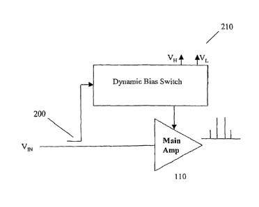
[0034] FIG. 3 illustrates a block diagram of an amplifier
from the feed-forward power amplifier system (or gain block)
having a dynamic bias switch unit 210 at the main amplifier
110. The amplifier may be a main amplifier 110 or an error
amplifier 160. As will be appreciated by those skilled in
the art, amplifiers 110 and 160 may each be made up of
multiple amplifier stages. The input signal from coupler
200 to main amplifier 110 is coupled to the dynamic bias
switch 210 via coupler 200. Coupler 200 is a conventionally
constructed coupler, known to those skilled in the art, for
sampling an input signal. The input signal typically
comprises multicarrier input signal having a signal envelope
with a large peak-to-average ratio.
CA 02505189 2005-05-05
WO 2004/049559 PCT/US2003/037499
13
[0035] The dynamic bias switch unit 210 generates an
output coupled to the amplifier 110 power supply. The
dynamic bias switch unit is configured to switch the power
supply level applied to the amplifier between a first power
supply level (VT) and a second power supply level (VL).
Alternating between the first power supply level and the
second power supply level improves amplifier efficiency so
that a high supply voltage is amplified only when needed,
and allows large dynamic range input signals to be amplified
with improved linearity.
[0036] As noted above, switching between supplies can
also reduce intermodulation products generated over that of
the method of continuously varying the power supplied to the
amplifier 110, that would be used in a system that attempts
to track the envelop of an RF input signal.
[0037] FIG. 4 is a time domain graph of an RF signal
level that is applied to the main amplifier, and a portion
of which is coupled to the dynamic bias unit by coupler 200.
As shown, the input signal typically will have a large peak-
to-peak average ratio. A Wide Band CDMA (WB-CDMA) signal
would be one example of such an input signal. The dynamic
bias switch analyzes the signal envelope of this input
signal to determine when a high voltage power supply needs
to be applied in order to sufficiently amplify the portion
of the signal with a high peak value.
[0038] High peak value signals typically cause distortion
in a power amplifier. When an amplifier is called upon to
amplify large valued signals the resulting amplifier would
be large, costly and consume large amounts of power. A
solution would be to use an amplifier designed to amplify
CA 02505189 2005-05-05
WO 2004/049559 PCT/US2003/037499
14
the signal level that is encountered most of the time with
sufficient linearity, and provide a way of boosting the
power handling capabilities of the amplifier when an
exceptionally strong signal is encountered.
[0039] One way to increase power handling is to attempt
to track the power supply needs of the amplifier after it is
determined that added power handling is needed, so that just
enough power is supplied to maintain linearity and
efficiency. Another way is to determine when increased
l0 power in the amplifier is needed, and switch the amplifier
to the single higher supply only when needed, thus keeping
amplifier efficiency up.
[0040] FIG. 5 is a time domain graph showing how the
dynamic bias switch switches the amplifier to a higher
supply voltage (VH) from a lower supply voltage (VI,) when a
threshold voltage (VT) has been exceeded by the RF input
signal (VIN) applied to the input of the dynamic bias
switch. As shown, the dynamic bias switch switches between
the first power supply level (VI,) and the second power
supply level (VII) when the signal envelope of the input
signal VIN exceeds a preset threshold. Specifically, the
dynamic bias switch switches between a lower voltage (VI,)
and a higher voltage (VH) in response to portions of the RF
input signal VIN that exceed the lower threshold (VT) to
produce the curve VDD .
[0041] In conventional high power amplification
techniques, a lower supply voltage was provided to the
amplifier until the peak of the RF input signal exceeded a
preset threshold, and then a higher amplifier bias voltage
was applied that tracked the signal envelope. The supply
CA 02505189 2005-05-05
WO 2004/049559 PCT/US2003/037499
voltage was made to track the signal envelope above the
threshold to supply just enough current to maintain
linearity while keeping power consumption down. However,
this approach would typically utilize a continuous voltage
5 controlled current source. The voltage controlled current
source would typically dissipate large amounts of power in
it's operation. For this stage of operation, amplification
would be linear, but inefficient.
[0042] By contrast, embodiments of the present invention
10 switch to the higher supply voltage with a low power
consumption pass-transistor switch when the signal envelope
of the RF input signal, that is detected by an envelope
detector, exceeds a preset threshold. This tends to be
beneficial because a switch tends to dissipate less power
15 than a voltage controlled current source. Thus, even though
the amplifier is continuously running at a higher current,
the overall efficiency is better than that obtained by
attempting to cut back amplifier power with an element that
has its own considerable power loss.
[0043] As shown, for input signal levels VIN falling
below the first signal level (VT) are sufficiently amplified
for a first percentage of time at first amplifier supply
voltage (VI,). During this first percentage of time 501 an
output waveform from the amplifier biased with VI, is free
from clipping.
[0044] An amplifier operating under bias of VI, and having
an input level VIN above first signal level (VT) has
insufficient linearity for a second percentage of time 503
during which VIN extends above the threshold line VT. The
second percentage of time 503 is generally statistically
CA 02505189 2005-05-05
WO 2004/049559 PCT/US2003/037499
16
less than the first percentage of time 501. Because the
second percentage of time 503 is statistically less than the
first percentage of time the first signal level is typically
adequate to operate the power amplifier and therefore power
losses can be reduced and the efficiency of the amplifier
can be improved.
[0045] To simplify this description, a first signal level
VI, and a second signal level VII will be described to
illustrate the basic function of the bias switching circuit
in response to the input signal VIN. In the time intervals
designated 501, the RF input to the amplifier has an
envelope describing the peak values of the RF waveform that
fall below the voltage level of VT. During time interval
501, the bias switch connects the amplifier to the bias
supply VH. The level VT is selected as will be ~ appreciated
by those skilled in the art so that the amplifier will
produce an output signal having sufficient linearity for the
intended use until VT is exceeded.
[0046] During the second time interval 503, the envelope
of the input signal VIN exceeds VT, as shown in the figure.
Rather than having the amplifier bias track VIN during this
portion of time, the bias to the amplifier is switched to a
higher level VH. The amplifier bias VDD remains at the VH
until the envelope of VIN falls below VT. V~Then VIN falls
below VT the bias switch switches the amplifier power supply
back to VI,.
[0047] It should be appreciated that these events occur
at high speeds. Those skilled in the art will realize that
high speed components having high switching speeds, fast
CA 02505189 2005-05-05
WO 2004/049559 PCT/US2003/037499
17
settling time, and low delays are called for in order to
implement the bias switch at high frequencies
[0048] However, one of ordinary skill in the art will
appreciate that the switching circuit 220 could be adapted
to switch between a plurality of signal levels in a similar
manner. For example, the switching circuit 220 could be
adapted to switch between a first signal level, a second
signal level, and a third signal level based on the signal
envelope. The switching circuit 220 could be adapted to
switch between any number of signal levels that would allow
switching that improves amplifier efficiency and provide
improved linearity while using a switch instead of a voltage
controlled current source.
[0049] FIG. 6 is a block diagram of an embodiment of a
dynamic bias switch. As shown, the dynamic bias switch unit
210 includes an extraction unit 230 for determining the
signal envelope, and a switching circuit 220 for switching
between the first power supply level VH and the second power
supply level VL based upon the input signal level.
[0050] A sample of the amplifier input signal VIN is
coupled to the input of the extraction unit 230. An output
of the extraction unit 230 is coupled to the input of the
switch circuit 220. The output of the switch circuit 220 is
coupled to the power supply input of the amplifier or gain
block (not shown). The switch circuit 220 includes a first
and second power supply input VH and VL, respectively. As
discussed above, the switching circuit 220 can switch
between the first power supply level and the second power
supply level when the signal envelope exceeds a preset
CA 02505189 2005-05-05
WO 2004/049559 PCT/US2003/037499
18
threshold VT, that is provided by a reference level internal
to the extraction unit.
[0051] The dynamic bias switch may be constructed on a
common circuit board with the gain block disposed at a
remote location. Alternatively, the dynamic bias switch may
be constructed as a discreet or integrated circuit disposed
on a substrate such as silicon, by methods known to those
skilled in the art.
[0052] FIG. 7 is a block diagram of an embodiment of the
l0 extraction unit of the dynamic bias switch. The extraction
unit includes a detector circuit 700 and a comparator
circuit 720. A sample of the amplifier input signal is
coupled to the input of the detector 700. The detector 700
is constructed in a manner known to those skilled in the art
to. extract the envelope from a sample of the multicarrier
input signal VIN.
[0053] The comparator circuit 720 has a first input
responsive to an output of the detector and a second input
responsive to a reference input signal. An output of the
detector 700 is coupled to the first input of comparator
circuit 720. The comparator circuit 720 generates an output
by comparing the output of the detector 700 with the
reference input signal. The output of the comparator
circuit 720 is coupled to the switch control unit 800 shown
in FIG. 8 (not shown). The comparator circuit is
constructed utilizing methods known to those skilled in the
art to produce a fast responding circuit with fast settling
time. In an embodiment, an evelope detector is used with a
comparator. In a further alternative embodiment, a very
fast peak detector is used.
CA 02505189 2005-05-05
WO 2004/049559 PCT/US2003/037499
I9
[0054] FIG. 8 is a block diagram of an embodiment of the
switch circuit of the dynamic bias switch. The switch
circuit 220 includes a switch control unit 800 and a pass
switch 820. The output of the comparator circuit is coupled
to the input of the switch control unit 800. The switch
control unit 800 is coupled to and responsive to an output
of the extraction unit (230 of FIG. 7), and generates an
output drive sufficient for controlling selection of one of
the first power supply levels, or the second power supply
level. An output of the switch control unit 800 is
coupled to the input of the pass switch 820. The pass
switch 820 is responsive to the output of the switch control
unit.
[0055] The pass switch 820 switches between power
supplies and generates an output comprising, for example,
the first power supply level or the second power supply
level, depending upon whether the signal envelope exceeds a
preset threshold. The output of the pass switch 820 is
coupled to the power supply input of the amplifier (not
shown) .
[0056] FIG. 9 is a schematic of an embodiment of the
dynamic bias switch. A dynamic bias switching circuit 900
includes a multicarrier signal input VIN, an extraction unit
230, and a switching circuit 220, as coupled and discussed
above .
[0057] The extraction unit 230 determines the signal
envelope. In the embodiment shown, the extraction unit 230
may be implemented using a detector 912 to generate an
envelope signal and a comparator circuit 301.
Alternatively, the detector circuit 912 may be eliminated,
CA 02505189 2005-05-05
WO 2004/049559 PCT/US2003/037499
as will be appreciated by those skilled in the art, if the
input characteristic of comparator 301 will allow direct
envelope detection.
[0058] The detector 912 can be an envelope detector that
5 is appropriate for use in high frequency amplification
applications. The frequency of envelope change in RF base
station applications is in the order of tens of megahertz.
Other types of detectors, such as a fast peak detector could
also be utilized so long as the detector is compatible with
10 switching at the megahertz range.
[0059] The output of the detector 912 is applied to a
positive input terminal 911 of a comparator circuit. A d-c
reference input VT, that may be changed with the
potentiometer that is supplied with a stable reference
15 voltage, is applied to another input 913 of the comparator
301. The comparator 301 can then be used to generate an
output by comparing the output of the detector 912 with a DC
reference input signal.
[0060] The comparator circuit is designed by methods
20 known to those skilled in the art to have very large voltage
gain. The comparator 301 can be implemented, in an
embodiment, using a fast operational amplifier 301 connected
in an open loop configuration. The operational amplifier
can have a first output voltage based on a first input
voltage level and a second output voltage based on a second
input voltage level. The dual positive and negative supply
voltages required to drive the operational amplifier 301 are
taken from VT and VH, or the separated sources.
[0061] The comparator output of the extraction unit 230
is coupled to the input of the buffer switch (or switch
CA 02505189 2005-05-05
WO 2004/049559 PCT/US2003/037499
21
control unit 800 as shown in FIG. 8) 910 of the switch
circuit 220. The switch unit 220 may be implemented, for
example, using a buffer switch 910 as the switch control
unit (800 of FIG.8) and a pass transistor 920 as the pass
switch (820 of FIG.8) . The buffer switch 910 enables fast
switching of pass-transistor 920 at speeds that are required
to match the envelope signal excursions above VT.
[0062] Those skilled in the art will appreciate that the
gate of transistor 920 posesses an inherent capacitance that
tends to limit the switching speed of the transistor 920.
Those skilled in the art will appreciate that in order for a
voltage sufficient to switch the transistor with little loss
to be reached, that the capacitor must be fully charged
quickly. A charging capacitor does not reach the voltage
applied to it until sufficient charge (supplied by a
current) has been supplied. The larger the capacitance that
may be required, the larger the amount of current that is
needed for fast switching. If the transistor does not switch
fast then the channel will be resistive, and thus lossy, for
an interval in time causing power loss. Thus, a high current
buffer that supplies a large amount of charge to the pass
transistor gate tends to switch the transistor quickly
between completely on and off states. Quick switching
reduces power dissipation in the pass transistor since the
channel of the pass transistor does not remain long in a
lossy state.
[0063] The buffer switch 910 may be implemented via a
push-pull circuit or in an alternative embodiment as a
single ended buffer circuit. However, a single ended circuit
tends to have increased loss due to the continuous presence
CA 02505189 2005-05-05
WO 2004/049559 PCT/US2003/037499
22
of a biasing resistor in the source connection. This
resistance and its power dissipation tends to be eliminated
by the dynamic load resistance of a complementary push pull
pair. For example in a single ended circuit a biasing
resistor would be utilized in the source or drain lead. Such
a resistor would always dissipate power. By utilizing a
complementary transistor the biasing resistor is not needed,
as will be appreciated by those skilled in the art.
[0064] In one embodiment, the push-pull circuit comprises
a pair of complementary transistors (shown in block 910).
The source terminal S of the first transistor 901A is
coupled to the positive supply voltage, and the source
terminal S of the second transistor 901B is coupled to the
negative supply voltage. The gates of each transistor 901A,
901B are coupled together and to node A which is coupled to
the output of a comparator 301. The drain terminals D of
each transistor 901A, 901B are coupled together at node B
which produces a voltage that drives the gate of pass
transistor 920.
[0065] As noted above, the frequency of envelope change
in RF base-station applications is in the order of tens of
megahertz. As such, faster switching MOS devices, such as
complementary MOSFET devices used in the buffer switch 910
can allow for large current switching at the megahertz
range, are utilized.
[0066] The output of the complementary-pair of MOSFET
transistors toggles between the first signal level (shown
here as a voltage level, VT) and the second signal level
(shown here as a voltage level, VH) and turns the pass
transistor 920 into 'ON' or 'OFF' states accordingly. As
CA 02505189 2005-05-05
WO 2004/049559 PCT/US2003/037499
23
such, the switching circuit 220 can generate an output that
includes, for example, one of the first signal level (VL)
and the second signal level (VH).
[0067] The first signal level can be, for example, a
discrete signal level (VL) generated by a diode circuit 304
when the pass transistor 920 is in an OFF state. The second
signal level (VH), can be, for example, a discrete signal
level (VH) when the pass transistor 920 is in an ON state.
[0068] In one embodiment, a source of pass transistor 920
is coupled to the positive supply voltage and the drain of
pass transistor 920 is coupled to node 960. The pass
transistor 920 is preferably configured such that when the
input signal envelope level exceeds a preset threshold, the
pass transistor is switched to the second signal level (VH)
when the signal envelope exceeds the preset threshold. This
places the pass transistor 920 in an ON state. In the ON
state the pass transistor is switched fully on, with little
channel resistance in the current path. Thus, little power
is dissipated in the pass transistor. The bias voltage used
to switch the pass transistor 920 to the second OFF state
tends to be preferably less than approximately one volt.
For example, in a ,p or n channel MOSFET, the bias voltage to
switch the transistor fully 'ON' has to be greater than 5
volts. In this mode of operation, the transistor channel
resistance is in the order of few hundredths of an ohm.
Thus, the pass transistor 920 can be operated as a switch
with extremely low channel (Ohmic) resistance in the path of
the current through the pass transistor. This tends to
provide a switching mode that can minimize power losses.
CA 02505189 2005-05-05
WO 2004/049559 PCT/US2003/037499
24
[0069] A drain and source of an RF transistor 940 of the
amplifier (not shown) is typically placed across terminals
960 and 980 by which two levels of VDD can be applied to the
RF transistor. The pass transistor 920 can be used to
control current between the power supply and a drain of the
RF transistor 940. The RF transistor 940 may comprise, for
example, high power transistors, such as, FETs or bipolar
devices.
[0070] One of two possible drain supply voltages, the
first signal level (VL) and the second signal level (VH) ,
can be utilized. By switching the drain voltage of the pass
transistor 920 to the second signal level (VH), the
transistor 920 is placed in an ON state when the signal
envelope exceeds the preset threshold (VT). The second
signal level (VH) can thus be applied to a drain of the RF
transistor 940 when the signal envelope exceeds the preset
threshold (VL) .
[0071] The improvement in efficiency of an amplifier
implementing the dynamic bias switch unit 900 results since
the product of current and the voltage across the active
device (e. g., the amplifier) which constitutes the energy
lost in the active device has been reduced. The pass
transistor 920, which is controlled by the input excitation,
is in 'ON' state only if the drain voltage VDD across the RF
transistor is insufficient to satisfy the swing of the input
voltage. Therefore, for most of the time, the lower supply
voltage is used and the energy loss is minimized. The pass
transistor 920 therefore serves as a switch as opposed to a
continuous voltage-controlled-current-source. The pass
transistor 920 can thus allow the higher supply voltage rail
CA 02505189 2005-05-05
WO 2004/049559 PCT/US2003/037499
to be applied to the drain of the RF transistor (not shown)
with negligible losses. The low power dissipation of the
switching-mode of the pass transistor is thus used to reduce
the losses and to improve the efficiency further.
5 [0072] The amplification of a Wide Band CDMA. (WB-CDMA)
signal is a typical application. Inspection of the
Complementary Cumulative Distribution Function. (CCDF) of
such a signal shows that for a considerable percentage of
time, the lower supply (VL) rail is sufficient to operate
10 the amplifier and the output waveform will not be clipped.
The drain voltage (VDD) is switched to a higher supply
voltage through switching circuitry when the envelope of the
input signal exceeds a preset threshold. Over the short
interval where high voltage (VH) is required, the pass
15 transistor 920 can be switched fully 'ON' and there is a
very little channel resistance (Ohmic resistance) in the
path of the current through the pass transistor 920. As a
result, power losses are minimized. Utilizing a switching
mode that avoids power losses can be beneficial to overall
20 amplifier efficiency.
[0073] FIG. 10 is a flow diagram showing a method for
linear amplification of a multicarrier signal in a feed-
forward power amplifier system, by switching between
amplifier power supplies based upon input signal,level.
25 [0074] At Block 1010, the power amplifier is connected to
the lower voltage power supply. At Blocks 1020, the input
signal envelope of VIN is sampled. At Block 1030, the
sample of the envelope of VIN is compared with a reference
signal. At Block 1040, it is determined if the signal
envelope exceeds a preset threshold VT.
CA 02505189 2005-05-05
WO 2004/049559 PCT/US2003/037499
26
[0075] If the signal envelope does not exceed the preset
threshold VT, then at Block 1050, the connection of the
power amplifier to the lower voltage power supply is
maintained. If the signal envelope exceeds a preset
threshold VT, then at Block 1060, the connection of the
power amplifier is switched to the higher voltage power
supply. Thus, the power supply input to the amplifier is
switched between a first signal level and a second signal
level, that is greater than the first signal level, if the
signal envelope exceeds a preset threshold to thereby track
variations of the envelope signal.
[0076] FIG. 11 illustrates a block diagram of an
amplifier and digital predistorter combination including a
dynamic bias switch. The dynamic bias switch is connected as
described above with respect to the main amplifier 110. In
this embodiment, however, a predistorter 111 is disposed
before the main amplifier 110. The input signal is received
directly by predistorter 111. The input signal typically
comprises multicarrier input signal having a signal envelope
with a large peak-to-average ratio.
[0077] The predistorter then processes the input signal
to generate an I (in-phase) and Q (quadrature) vector with
information about the Cartesian coordinates that describe
the input signal. These Cartesian coordinates can be
converted into polar coordinates specifying amplitude
information and phase information. This information can
then be used by the dynamic bias switch 210 to generate VH
and VL., and by amplifier 110. The predistorter is a
conventionally constructed predistorter, constructed
utilizing techniques known to those skilled in the art.
CA 02505189 2005-05-05
WO 2004/049559 PCT/US2003/037499
27
Equivalently, other distortion reducing circuits and methods
may be used in conjunction with the dynamic bias switch to
reduce the overall amplifier system distortion.
[0078] In FIG. 12, the input signal from coupler 200 to
main amplifier 110 is coupled to the dynamic bias switch 210
via coupler 200. The predistorter utilized in this
embodiment is a conventionally constructed analog
predistorter, constructed utilizing methods known to their
skilled in the art. Likewise, sampling circuit 200 shown
as a directional coupler, may be equivalently constructed
utilizing methods known to those skilled in the art to
sample the desired signals.
[0079] FIG. 13 illustrates a block diagram of an
amplifier including a dynamic bias switch with a delay
circuit disposed in front of the amplifier. The dynamic
bias switch is connected as described above with respect to
the amplifier 110. In this embodiment, however, a delay
circuit 112 is disposed before the amplifier 110 and after
the sampling circuit 200, such that the input signal is
delayed before being coupled to the amplifier 110. The
delay circuit 112 tends to compensate for time delays
introduced by the dynamic bias switch 210.
[0080] To synchronize the amplitude modulations and
correct reconstruction of the original input signal, the
delay between the amplifier input to opuput path and the
samplig circuit to the output of the dynamic bias switch
should be equalized as much as possible. Introducing the
dynamic bias switch unit can cause the time delay in the RF
phase path to be substantially shorter than that of the low
frequency amplitude information.
CA 02505189 2005-05-05
WO 2004/049559 PCT/US2003/037499
28
[0081] The shorter wavelengths associated with high
frequencies, such as RF frequencies, allow a delay circuit
to be practical. At low frequencies, such as audio
frequencies, a delay circuit would be too large.
[0082] This mismatch in time delay can cause increased
distortion to appear at the output of the main amplifier.
The intermodulation distortion (IMD) introduced by delay
mismatch is given by:
10083] azn~ 2~r ~B2RF) (OTZ~
[0084] where BRF is the signal bandwidth and DT is the
delay mismatch. Thus, to reduce the distortion it is
expedient to reduce the time delay to zero by equalizing the
path lengths.
(0085] The delay circuit 112 provides time delay
equalization to help reduce IMD. The delay circuit 112 may
be implemented, for example, by a low-loss coaxial cable
(delay line) or any other slow wave structure .of suitable
electrical length.
[0086] In alternate embodiments of amplifier systems that
implement the dynamic bias switch unit, multiple stages of
amplification are disposed between the sampling circuit 200
and the amplifier that is controlled by the dynamic bias
switch 200. These multiple stages of amplification provide
additional drive for the final amplifier which is controlled
by the dynamic bias switch. The RF input sampling that
provides the envelope information is taken at the input of
the amplifier before the driver stages and other passive and
active circuits. The delay in driver (RF) amplifier chain
will aid the time alignment between the slower-path of
envelope-triggered switching action and the RF signal in the
CA 02505189 2005-05-05
WO 2004/049559 PCT/US2003/037499
29
power stages. One or more additional delay lines will
compensate the differential delay that remains.
[0087] While aspects of the present invention have been
described in terms of certain preferred embodiments, those
of ordinary skill in the will appreciate that certain
variations, extensions and modifications may be made without
varying from the basic teachings of the present invention.
For example, although the dynamic bias switch has been
described with respect to the application to amplifiers,
those skilled in the art will realize that it may also be
applied to other types of non-linear circuits. that would
benefit from power supply switching to improve their
linearity and reduce distortion. As such, aspects of the
present invention are not to be limited to the specific
preferred embodiments described herein. Rather, the scope
of the present invention is to be determined from the
claims, which follow.