Note: Descriptions are shown in the official language in which they were submitted.
CA 02505256 2012-01-20
OPTICAL COMPONENT FOR FREE-SPACE OPTICAL
PROPAGATION BETWEEN WAVEGUIDES
1
CA 02505256 2005-05-05
WO 2004/044622 PCT/US2003/032207
BACKGROUND
[0002] The field of the present invention relates to optical components. In
particular, reflective and/or transmissive optical components are disclosed
herein
for free-space optical propagation between waveguides.
[0003] Planar optical waveguides are suitable for implementing a variety of
optical
devices for use in telecommunications and other fields. In addition to the
planar
waveguides, the planar waveguide substrate often also includes (by fabrication
and/or placement thereon): alignment/support structures for placement of
optical
components/devices on the substrate; V-grooves and/or other alignment/support
structures for positioning of optical fibers and/or fiber-optic tapers on the
substrate;
compensators, gratings, filters, and/or other optical elements/devices;
electrical
contacts and/or traces for enabling electronic access to active devices on the
substrate; and/or other suitable components. Reflective and/or transmissive
optical
elements including, but not limited to, mirrors, beamsplitters, beam
combiners,
filters, lenses, and so forth are disclosed herein for use with one or more
planar
optical waveguides and for free-space optical propagation and/or end-coupling
therebetween.
2
CA 02505256 2012-01-20
SUMMARY
[0004] The present invention provides an optical apparatus comprising: a
horizontal member; two side walls integrally formed with and protruding from
the
horizontal member; a substantially transparent end wall integrally formed with
and
protruding from the horizontal member, the end wall, side walls, and
horizontal
member partially enclosing an interior volume; and optical functionality
imparted on
at least a portion of the end wall, wherein the two side walls are arranged
for
engaging a substantially horizontal mounting surface so as to position the end
wall
at a desired angle with respect to the mounting surface and so that the
mounting
surface partially encloses the interior volume opposite the horizontal member.
[00051 The optical component may be formed on a substrate, with a portion of
the
substrate forming the horizontal member and with the side walls and end wall
protruding from the substrate. The optical apparatus may instead be formed on
a
substrate, with the end wall comprising an optical component layer formed on
the
substrate with substrate material then removed from beneath it. The side walls
and
horizontal member are formed from substrate material separated from the rest
of
the substrate along with the optical component layer. Either of these methods
may
be implemented on a wafer scale for concurrent fabrication of many optical
components. Optical functionality may be imparted on a wafer scale, at the bar
level, and/or at the individual component level.
[0006] There is also provided an optical apparatus comprising: a planar
optical
waveguide formed on a waveguide substrate; a second optical waveguide
positioned on the waveguide substrate and optically end-coupled with the
planar
optical waveguide; and an optical component, comprising (i) a horizontal
member,
(ii) two side walls integrally formed with and protruding from the horizontal
member,
(iii) a substantially transparent end wall integrally formed with and
protruding from
the horizontal member, the end wall, side walls, and horizontal member
partially
enclosing an interior volume; and (iv) optical functionality imparted on at
least a
portion of the end wall, wherein: the two side walls are arranged for engaging
the
3
CA 02505256 2012-01-20
waveguide substrate so as to position the end wall at a desired angle with
respect
to the waveguide substrate and so that the waveguide substrate partially
encloses
the interior volume opposite the horizontal member; the optical component is
mounted on the waveguide substrate with the two side walls engaged therewith;
and the planar optical waveguide and the second optical waveguide are
optically
end-coupled by reflection from the optical component end wall or by
transmission
through the optical component end wall.
[0006a] There is also provided an optical apparatus comprising: a substrate;
at
least three planar optical waveguides formed on the substrate; at least one
laser
mounted on the substrate for emitting optical power at an output wavelength;
at
least one photodetector mounted on the substrate for detecting optical power
at an
input wavelength; and at least one optical component mounted on the substrate,
wherein: a first one of the planar waveguides is optically end-coupled at a
first end
face thereof with a second one of the planar waveguides at an end face
thereof; the
first planar waveguide is optically end-coupled at the first end face thereof
with a
third one of the planar waveguides at an end face thereof; the optical
component
directs optical power emerging from the end face of the second planar
waveguide
into the first end face of the first planar waveguide; the optical component
directs
optical power emerging from the first end face of the first planar waveguide
into the
end face of the third planar waveguide; the laser is optically coupled to the
second
planar waveguide so that optical output power emitted by the laser propagates
along the second planar waveguide and emerges through the end face thereof;
the
photodetector is optically coupled to the third planar waveguide so that
optical input
power entering the end face thereof propagates along the third planar
waveguide
for detection by the photodetector; the optical component comprises a
horizontal
member with two side walls and a substantially transparent end wall integrally
formed therewith and each protruding therefrom and partially enclosing an
interior
volume, and a spectrally-selective optical filter coating formed on at least
one
surface of the end wall, the two side walls being arranged for engaging the
substrate so as to position the end wall at a desired angle with respect to
the
4
CA 02505256 2012-01-20
substrate and so that the substrate partially encloses the interior volume
opposite
the horizontal member; and the optical component is mounted with the two side
walls engaged with the substrate, with the end wall near the waveguide end
faces,
and with at least one of the waveguide end faces received within the interior
volume.
[0006b] In a further aspect, there is provided a method comprising: integrally
forming on a horizontal member two side walls and a substantially transparent
end
wall, the end wall and the side walls protruding from the horizontal member,
the end
wall, side walls, and horizontal member partially enclosing an interior
volume; and
imparting optical functionality on at least a portion of the end wall, wherein
the two
side walls are arranged for engaging a substantially horizontal mounting
surface so
as to position the end wall at a desired angle with respect to the mounting
surface
and so that the mounting surface partially encloses the interior volume
opposite the
horizontal member.
[0006c] In a further aspect, there is provided a method comprising: forming a
substantially transparent optical component layer over a component area on a
first
surface of a substrate; forming a passage from the first substrate surface
through
the substrate adjacent to the component area; removing substrate material from
a
second substrate surface over an area thereof opposite the component area so
as
to remove substrate material from the optical component layer and form an
interior
volume partially enclosed by the optical component layer and three substrate
side
walls, the interior volume being contiguous with the passage; separating the
optical
component layer and the three substrate side walls from the substrate, the
optical
component layer remaining connected to adjacent portions of at least two of
the
substrate side walls; and imparting optical functionality on at least a
portion of the
optical component layer.
[0006d] In a further aspect, there is provided a method comprising:
propagating an
optical signal in a first optical waveguide positioned on a waveguide
substrate;
transmitting the optical signal out of the first optical waveguide through an
end face
4a
CA 02505256 2012-01-20
thereof; receiving, into a second optical waveguide positioned on the
waveguide
substrate and optically end-coupled with the first optical waveguide, through
an end
face of the second optical waveguide, at least a portion of the optical signal
that is
transmitted through the end face of the first optical waveguide, the received
portion
of the optical signal being reflected by or transmitted through an end wall of
an
optical component; and propagating in the second optical waveguide that
portion of
the optical signal received through the end face thereof, wherein: the optical
component comprises (i) a horizontal member, (ii) two side walls integrally
formed
with and protruding from the horizontal member, (iii) the end wall integrally
formed
with and protruding from the horizontal member, the end wall, side walls, and
horizontal member partially enclosing an interior volume, and (iv) optical
functionality imparted on at least a portion of the end wall; and the two side
walls
are arranged for engaging the waveguide substrate so as to position the end
wall at
a desired angle with respect to the waveguide substrate and so that the
waveguide
substrate partially encloses the interior volume opposite the horizontal
member, and
the optical component is mounted on the waveguide substrate with the two side
walls engaged therewith.
[0006e] In a further aspect, there is provided a method comprising:
propagating an
input optical signal in a first planar optical waveguide formed on a waveguide
substrate; propagating, in a second planar optical waveguide formed on the
waveguide substrate and optical end-coupled with the first planar optical
waveguide, an output optical signal received from a laser mounted on the
waveguide substrate; transmitting the input optical signal out of the first
optical
waveguide through an end face thereof; transmitting the output optical signal
out of
the second optical waveguide through an end face thereof; receiving, into a
third
optical waveguide positioned on the waveguide substrate and optically end-
coupled
with the first optical waveguide, through an end face of the third optical
waveguide,
at least a portion of the input optical signal that is transmitted through the
end face
of the first optical waveguide, the received portion of the input optical
signal being
directed between the first and third planar optical waveguides by an optical
4b
CA 02505256 2012-01-20
component, the optical component comprising (i) a horizontal member, (ii) two
side
walls integrally formed with and protruding from the horizontal member, (iii)
an end
wall integrally formed with and protruding from the horizontal member, the end
wall,
side walls, and horizontal member partially enclosing an interior volume, and
(iv)
optical functionality imparted on at least a portion of the end wall, wherein
the two
side walls are arranged for engaging the waveguide substrate so as to position
the
end wall at a desired angle with respect to the waveguide substrate and so
that the
waveguide substrate partially encloses the interior volume opposite the
horizontal
member, and the optical component is mounted on the waveguide substrate with
the two side walls engaged therewith; receiving, into the first optical
waveguide
through the end face thereof, at least a portion of the output optical signal
that is
transmitted through the end face of the second planar optical waveguide, the
received portion of the output optical signal being directed between the first
and
second planar optical waveguides by the optical component; propagating in the
third
planar optical waveguide to a photodetector mounted on the waveguide substrate
that portion of the input optical signal received through the end face of the
third
planar optical waveguide; and,propagating in the first planar optical
waveguide that
portion of the output optical signal received through the end face thereof.
[0007] Features and advantages of optical components and/or assemblies
disclosed herein may become apparent upon referring to the disclosed exemplary
embodiments as illustrated in the drawings and set forth in the following
written
description.
4c
CA 02505256 2005-05-05
WO 2004/044622 PCT/US2003/032207
BRIEF DESCRIPTION OF THE DRAWINGS
[0008] Fig. 1 is a schematic top view of a generic optical assembly.
[0009] Fig. 2 is a schematic top view of a generic optical assembly.
[0010] Figs. 3A and 3B are schematic top and elevation views, respectively, of
a
generic optical assembly.
[0011] Figs. 4A and 4B are schematic top and elevation views, respectively, of
a
generic optical assembly.
[0012] Figs. 5A, 5B, 5C, and 5D are top, end, side, and isometric views,
respectively, of an exemplary optical component.
[0013] Figs. 6A, 6B, 6C, and 6D are top views of exemplary optical components
and waveguides.
[0014] Figs. 7A and 7B are schematic top and elevation views, respectively, of
an
exemplary optical assembly. Fig. 7C is a schematic elevation view of an
exemplary optical assembly.
[0015] Figs. 8A and 8B are schematic top and elevation views, respectively, of
an
exemplary optical assembly. Fig. 8C is a schematic elevation view of an
exemplary optical assembly.
[0016] Fig. 9 is a schematic top view of an exemplary optical assembly.
[0017] Fig. 10 is a schematic top view of an exemplary optical assembly.
[0018] Figs. 11 A and 11 B are top views of exemplary dual optical components
and
waveguides.
[0019] Figs. 12A. 12B, 12C, 13A, and 13B illustrate exemplary process
sequences
for fabricating optical components.
[0020] Figs. 14A and 14B are schematic isometric views of exemplary optical
components.
[0021] Figs. 15A, 15B, and 15C are plan and cross-sectional views of optical
waveguides.
[0022] Fig. 16 is a schematic top view of an exemplary optical assembly.
5
CA 02505256 2012-01-20
[0023] It should be noted that the relative proportions of various structures
shown
in the Figures may be distorted to more clearly illustrate the present
invention.
Relative dimensions of various optical devices, optical waveguides, optical
fibers,
optical components, optical modes, alignment/support members, grooves, and so
forth may be distorted, both relative to each other as well as in their
relative
transverse and/or longitudinal proportions. In many of the Figures the
transverse
dimension of an optical element is enlarged relative to the longitudinal
dimension for
clarity, which will cause variations of transverse dimension(s) with
longitudinal
position to appear exaggerated.
[0024] Aspects of the present invention are illustrated in the Figures merely
by way
of example.
6
CA 02505256 2005-05-05
WO 2004/044622 PCT/US2003/032207
DETAILED DESCRIPTION OF EMBODIMENTS
[0025] Many of the optical waveguides (including both optical fibers and
planar
waveguides) described herein have dimensions and design parameters so as to
support only one or a few lowest-order optical modes. At visible and near-IR
wavelengths, the resulting optical modes are typically a few pm up to about 10
or
m in transverse extent. Depending on the nature of the waveguide, the guided
optical mode(s) may be nearly cylindrically symmetric, or may differ
substantially in
transverse extent along substantially orthogonal transverse dimensions. Modes
of
these wavelengths and sizes typically exhibit substantially diffractive
behavior
1o beyond the end face of the supporting waveguide, typically becoming
substantially
convergent/divergent sufficiently far from the end face of the supporting
waveguide
(NA often greater than about 0.1). Accordingly, one or more of the following
adaptations may be required to achieve a degree of optical power transfer
above
an operationally acceptable level between end-coupled waveguides: maintain the
15 unguided optical pathlength between the waveguide end faces as small as
practicable for a particular optical assembly; adapt the end portion of one or
both
waveguides for mitigating the diffractive behavior of the optical mode at the
end
face of the waveguide; insert one or more additional optical elements between
the
waveguides for refocusing, re-imaging, or otherwise manipulating the mode
spatial
properties for enhancing end-coupling between the waveguides.
[0026] It is often the case in a waveguide-based optical system or waveguide-
based multi-component optical device that optical functionality is to be
provided that
cannot be readily implemented within a waveguide, and must therefore be
provided
by an optical component (reflective and/or transmissive) interposed in the
optical
path between end faces of waveguides, with unguided (i.e., free-space) optical
propagation between the waveguides (reflected from a reflective optical
component
and/or transmitted through a transmissive optical component). In order to
implement optical functionality in this way while maintaining overall
transmission
through the optical system at or above an operationally acceptable level, it
is
typically necessary to adapt the optical system or multi-component optical
device
as described in the preceding paragraph.
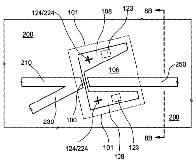
[0027] Fig. 1 is a schematic diagram of an optical assembly including an
optical
component 100 positioned on a planar waveguide substrate 200 along with
optical
7
CA 02505256 2005-05-05
WO 2004/044622 PCT/US2003/032207
waveguides 210, 230, and 250, at least one of which is a planar waveguide
formed
on substrate 200. Optical power may propagate through each of waveguides
210/230/250 in one or more of the respective propagating modes supported
thereby. Each waveguide 210/230/250 terminates at respective end faces
211/231/251, through which optical power may enter/exit the respective
waveguide
by end-transfer of optical power (equivalently: end-transfer, end coupling,
end-
coupled optical power transfer, end-coupled transfer of optical power, end-
coupled
transfer) with respective freely propagating optical beams 10/30/50 (freely
propagating indicating lack of transverse guiding as provided by a waveguide).
Waveguides 210 and 230 and optical component 100 may be suitably arranged so
as to enable reflectively-coupled end-transfer of optical power between
waveguides
210 and 230 by reflection of optical beams 10 and/or 30 from surfaces 102
and/or
104 of optical component 100 (including double-pass transmission through
component 100 for reflection from surface 104; reflection only from surface
102
depicted in Figs. 1, 2, 3A/3B, and 4A/4B). Similarly, waveguides 210 and 250
and
optical component 100 may be suitably arranged so as to enable transmissively-
coupled end-transfer of optical power between waveguides 210 and 250 by
transmission of optical beams 10 and/or 50 through optical component 100 and
surfaces 102 and 104 thereof.
[0028] Optical component 100 may be adapted in myriad ways for modifying the
intensity, spatial characteristics, polarization characteristics, and/or
spectral
characteristics of optical beams reflected therefrom and/or transmitted
therethrough
(i.e., for imparting optical functionality on the optical component). The
generic
optical assembly of Fig. 1 may therefore be employed for implementing a wide
array of optical functionality via optical component 100 (which may also serve
to
enhance end-coupling between the waveguides) while remaining within the scope
of the present disclosure and/or the appended claims. Examples of imparting
optical functionality may include, but are not limited to: i) forming at least
one
optical coating on at least one surface of the optical component; ii)
providing the
optical component with at least one curved surface; iii) providing at least
one
surface of the optical component with a spatially-varying surface profile; iv)
providing the optical component with at least one spatially-varying optical
property;
v) providing the optical component with at least one anisotropic optical
property;
8
CA 02505256 2005-05-05
WO 2004/044622 PCT/US2003/032207
and/or vi) providing the optical component with at least one spectrally-
varying
optical property. More specific examples of adaptations of optical component
100
for imparting optical functionality may include (without being limited to):
spatial
orientation of surfaces 102/104; curvature in one or two dimensions of one or
both
of surfaces 102/104; surface discontinuities (such as facet boundaries) on one
or
both of surfaces 102/104; reflective, partially reflective, and/or anti-
reflective
coatings on one or both of surfaces 102/104; diffractive structures
implemented on
one or both of surfaces 102/104 and/or within component 100; refractive index
spectral and/or spatial discontinuities, gradients, and/or modulations within
1o component 100; birefringent and/or dichroic properties (with respect to
linear and/or
circular polarization) within component 100; birefringent and/or dichroic
coatings
(with respect to linear and/or circular polarization) on one or both of
surfaces
102/104; Faraday rotation within component 100; optical
absorption/transmission
within component 100; spectral and/or spatial discontinuities, gradients,
and/or
modulations of any one or more of the foregoing. Such adaptations of optical
component 100 may be position dependent or independent, may be wavelength
dependent or independent, and may be polarization dependent or independent, as
needed for implementation of particular functionalitie(s) to be provided by
the
optical assembly of Fig. 1.
[0029] At least one of waveguides 210/230/250 may be implemented as a planar
waveguide formed on substrate 200. If all three waveguides are planar
waveguides
formed on substrate 200, spatially-selective material processing techniques
may be
employed for sufficiently accurate positioning (within operationally
acceptable
tolerances) of the waveguides on the substrate for enabling intended
functionality of
the optical assembly. If one or two of waveguides 210/230/250 are not planar
waveguides on substrate 200, substrate 200 may be adapted for suitably
mounting
such waveguide(s) relative to planar waveguide(s) thereon for enabling (within
operationally acceptable tolerances) intended functionality of the optical
assembly.
For example, one or two of waveguides 210/230/250 may comprise an optical
fiber
(waveguide 250, for example, as shown schematically in Fig. 2). Substrate 200
may be provided with corresponding V-groove(s) 201, alignment edge(s) 202,
and/or other suitable alignment structure(s) for enabling sufficiently
accurate
passive positioning (as opposed to active positioning, in which functioning of
the
9
CA 02505256 2005-05-05
WO 2004/044622 PCT/US2003/032207
optical assembly or sub-assembly thereof is monitored to determine positional
accuracy) of the optical fiber(s) relative to the planar waveguide(s) (within
operationally acceptable tolerances). In another example, one or two of
waveguides 210/230/250 (waveguide 230, for example, as shown schematically in
Figs. 3A/3B) comprises a planar waveguide formed on a corresponding separate
waveguide substrate 239. Substrate 200 and/or substrate 239 may be provided
with suitable support/alignment structures 203 and 233, respectively, for
enabling
sufficiently accurate passive positioning (within operationally acceptable
tolerances)
of waveguide 230 relative to waveguides 210/250. Alternatively, substrate 200
may
1o be provided with support structure(s) 205 and substrates 200 and 239 may be
provided with alignment marks 204 and 234, respectively, for enabling
sufficiently
accurate vision-based passive positioning (human vision or machine vision;
within
operationally acceptable tolerances) of waveguide 230 relative to waveguides
210/250 (shown schematically in Fig. 4).
[0030] Optical component 100 may be adapted for enabling sufficiently accurate
passive positioning (within operationally acceptable tolerances) on substrate
200
relative to waveguides 210/230/250 and for in turn enabling intended
functionality of
the optical assembly. An embodiment of component 100 suitable for placement on
substrate 200 near an end face of a planar waveguide (waveguide 250, for
example) is shown in Figs. 5A/5B/5C/5D. Optical component 100 is shown formed
on a component substrate that has been spatially-selectively processed to form
a
partially enclosed pocket or interior volume 106 between side walls 108, a
horizontal member 101, and an end wall, the end wall forming optical component
100. The optical component 100 includes in this exemplary embodiment
substantially flat, substantially vertical inner and outer surfaces 102 and
104,
respectively. The other end of the interior volume 106 is left open in this
example.
Horizontal member 101 extends beyond optical component 100 and side walls 108
in this example, but this need not be the case.
[0031] Use of a substantially homogeneous material for forming component 100
results in substantially uniform optical properties within component 100,
while use
of an inhomogeneous material (having one or more spatial discontinuities,
gradients, and/or modulations) results in similarly inhomogeneous properties
within
component 100. Component 100, horizontal member 101, and side walls 108 may
CA 02505256 2005-05-05
WO 2004/044622 PCT/US2003/032207
be formed by spatially-selective processing of the substrate material.
Alternatively,
an overlayer comprising one or more different materials maybe applied to a
substrate and spatially-selectively processed to form component 100 and side
walls
108; in this case horizontal member 101 may comprise one or both of substrate
material and overlayer material(s). Optical component 100 may be as thin as
practicable for maintaining structural integrity without requiring excessive
separation between ends of waveguides 210/230/250. Component 100 may
typically range between about 10 m and about 50 gm in thickness, often
between
about 20 gm and about 30 m. Thinner optical components may be employed if
fabricated from sufficiently robust material(s) and handled with sufficient
care.
Thicker optical components 100 may be employed (up to 100 m or more) if
necessary or desirable for implementing particular optical functionality,
and/or for
laterally off-setting reflected beams from the two component surfaces in an
off-
normal incidence geometry. One or both of surfaces 102/104 may be provided
with
an optical coating for providing optical functionality. Spatially selective
material
processing may be employed to provide one or more of: one or more alignment
edges and/or vertical and/or horizontal alignment surfaces on side walls 108
and/or
horizontal member 101 for engaging corresponding alignment/support structures
on
waveguide substrate 200; one or more alignment marks 124 for enabling vision-
2o based positioning of component 100 on correspondingly marked waveguide
substrate 200; and/or one or more solder pads 123 for securing component 100
to
substrate 200.
[0032] After fabrication, horizontal member 101 with optical component 100
thereon is inverted, positioned on substrate 200, and secured thereto using so-
called "flip-chip" mounting (as shown in Figs. 7A/7B and 8A/8B). In order to
reduce
the distance separating the ends of waveguides 210/230/250 (thereby somewhat
mitigating diffractive end-coupling losses that may be present) while
nevertheless
accommodating optical component 100 and secure mounting/support thereof on
substrate 200, at least an end portion of one of the planar waveguides
(waveguide
250 in the illustrated examples) may form a ridge protruding from an adjacent
area
of substrate 200, so that upon flip-chip mounting of optical component 100 on
substrate 200, the end portion of waveguide 250 is received within pocket 106
with
surface 104 of optical component 100 near end face 251 of waveguide 250 (Figs.
11
CA 02505256 2005-05-05
WO 2004/044622 PCT/US2003/032207
6A/6B/6C/6D). Pocket or interior volume 106 may range from about 10 m in
height up to several tens of m high or more to accommodate typical planar
waveguides, and may be made any suitable width required to accommodate a
planar waveguide. The width of pocket 106 and/or the positions/orientations of
side
walls 108 thereof may be configured to permit placement of optical component
100
at a required angle (within operationally acceptable tolerances; as
illustrated in the
examples of Figs. 6A/6B/6C/6D, 7A/7B, and 8A/8B) relative to waveguide 250
(and
therefore also waveguides 210/230). To reduce diffractive losses while
facilitating
mounting of component 100 between the waveguides, the waveguides may be
positioned on the substrate so that upon mounting of the optical component
100,
each of the waveguide end faces is within about 5 m of a facing component
surface 102 or 104. Larger separations between the waveguide end faces and the
optical component surfaces may also fall within the scope of the present
disclosure
and/or appended claims.
[0033] Fig. 6A shows an example of an optical component at substantially
normal
incidence with respect to component 100, with the end face of the waveguide
also
at substantially normal incidence. Fig. 6B shows a non-normal optical
component
with a substantially normal waveguide end face. End faces of waveguides 210,
230, and/or 250 may be adapted for enabling close positioning of a non-normal
optical component 100 without excessive separation between the waveguides. In
the examples of Figs. 6C/6D, 7A/7B, and 8A/8B the end faces are angled (i.e.,
not
substantially orthogonal to the propagation direction of the respective
waveguide),
thereby allowing a non-normal optical component 100 to be positioned closer to
end faces of each of the waveguides.
[0034] In order to reduce unwanted reflective losses at waveguide end faces
and
at any nominally non-reflective surface of component 100 (when the
waveguide(s)
and optical component are of similar refractive index), an index-matched
embedding medium may be interposed between the waveguide end faces and the
surfaces of the optical component. This may be accomplished by embedding the
3o assembled waveguides and optical component in a substantially index-matched
embedding medium, such as a polymer. A solution or suspension of polymer
precursor is applied and flows into spaces between optical surfaces. After
curing of
the polymer, the waveguides and optical component and waveguides are
12
CA 02505256 2005-05-05
WO 2004/044622 PCT/US2003/032207
embedded. In order to facilitate flow of the index-matching (or "potting")
medium
between the inner surface 104 of the optical component and the end face of the
waveguide received in the pocket of the optical component, one or more
openings
may be provided through one or both side walls 108, around component 100 on
the
end wall, and/or through component substrate 101. Even if waveguide and
component materials have substantially differing refractive indices, an
embedding
material may still reduce unwanted reflective losses (relative to air or
vacuum).
[0035] If only transmissively-coupled end-transfer is intended, an optical
component fabricated as disclosed herein may be employed at normal or near
1o normal incidence (illustrated in Fig. 6A), although non-normal incidence
may be
employed as well. Optical components for which only transmissive optical
functionality may be required may include spectral notch, short-pass, long-
pass,
and/or bandpass filters, for example, intended to reject one or more incident
spectral components that need not be directed elsewhere. Such functionality
may
be readily provided by one or more optical coating(s) on one or both of
surfaces
102 and 104 of optical component 100. Other examples of transmissive-only
optical components may fall within the scope of the present disclosure and/or
appended claims. Non-normal incidence with respect to component 100 (as
illustrated in Figs. 6B/6C/6D, 7A/7B, and 8A/8B) typically may be required for
including reflectively-coupled end-transfer. Such components may include as
examples the various spectral filter types mentioned hereinabove, in which the
rejected spectral component(s) must be directed to a specific location. Other
examples of transmissive plus reflective optical functionality may fall within
the
scope of the present disclosure and/or appended claims.
[0036] It may be desirable to suppress at least a portion of unwanted light
reflected, transmitted, and/or scattered by optical component 100. For
example, a
fraction of light emerging from waveguide 230 and reflected from optical
component
100 into waveguide 210 may leak through component 100. Given the angular
misalignment of waveguides 230 and 250, it may be unlikely in many cases that
a
significant amount of this unwanted transmitted light would enter waveguide
250. It
may nevertheless be desirable to reduce the amount of such leakage light
reaching
other components or devices on substrate 200. Side walls 108 may be adapted
for
absorbing such unwanted light (at an operating wavelength for component 100)
13
CA 02505256 2005-05-05
WO 2004/044622 PCT/US2003/032207
transmitted through component 100 from waveguide 230, for example.
Alternatively, as shown in Figs. 7C and 8C, side walls 108 may be tilted and
suitably coated so as to reflect such unwanted transmitted light downward into
the
substrate 200, to be absorbed or transmitted away from components on the
substrate surface. These adaptations may also serve to suppress unwanted
reflection from component 100 of light emerging from waveguide 250 for
transmission through component 100 and into waveguide 210. Alternatively, an
additional waveguide 270 may be positioned on substrate 200 for receiving
unwanted transmitted or reflected optical signals (from waveguides 230 and
250,
respectively), as shown in Fig. 16. Such a "beam dump" waveguide may convey
unwanted light away from sensitive components on substrate 200, or may be
adapted in any suitable manner for absorbing or dissipating the unwanted
light. It
should be noted that the exemplary embodiment of Fig. 16 may also be employed
for implementing a four-port optical assembly, in which any or all of
waveguides
210, 230, 250, and/or 270 may be used for transmitting and/or receiving
optical
signals reflected and/or transmitted by component 100.
[0037] Reflectively-coupled end-transfer may be implemented at any suitable
angle of incidence on optical component 100. Many optical coatings and/or
components exhibit properties which vary with angle of incidence, and which
may
have wavelength and/or polarization dependences that in turn depend on angle
of
incidence (further complicated by the range of incident angles present in a
convergent or divergent incident beam). These dependences are typically at a
minimum near normal incidence and increase with increasing angle of incidence,
which may in some instances impose an upper limit on the angle of incidence
that
may be used for a given optical component 100. A lower limit for a usable
angle of
incidence may be determined in part by the degree of diffractive losses that
may be
tolerated in the optical assembly. In Figs. 7A and 8A, waveguides 210 and 230
are
shown merging as they approach component 100. Parasitic optical losses
increase
with increasing length of the merged portion of the waveguides, which in turn
increases with decreasing angle of incidence (and therefore a decreased angle
of
separation between the waveguides). In any given assembly the optical
performance required (which may be degraded by a larger angle of incidence)
may
be balanced against optical loss induced by the merged section of the
waveguides
14
CA 02505256 2005-05-05
WO 2004/044622 PCT/US2003/032207
(typically worsened by a smaller angle of incidence). Geometric and space
constraints on the waveguide substrate may also come into play. A range of
compromise values is typically available for a particular optical assembly
incorporating particular optical functionality via the optical component 100.
Many
optical assemblies may have an incidence angle below about 45 (i.e.,
reflectively
coupled waveguides forming an angle less than about 90 ), often between about
7
and about 18 (i.e., reflectively coupled waveguides forming an angle between
about 15 and about 35 ). However, any suitable angle of incidence on optical
component 100 (and corresponding angle between reflectively coupled waveguide)
1o shall fall within the scope of the present disclosure and/or appended
claims.
[0038] A waveguide having a thin core (i.e., less than about 3 m high, often
less
than about I pm high) may be employed for reducing optical losses at small
incidence angles on optical component 100, as shown in Figs. 15A-15C. The
presence of one of the cores 212 and 232 gives rise to parasitic optical loss
in the
other, and this parasitic loss is roughly proportional to the cross-sectional
area of
the interfering core. For given optical mode sizes supported by waveguides 210
and 230, reducing the cross-sectional area of the respective cores 212 and 232
correspondingly reduces the level of parasitic optical loss from one core
induced by
the other. For a given angle between the waveguides, use of thin waveguide
cores
(as shown in the cross-section of Fig. 15C) reduces parasitic optical losses
relative
to thicker waveguide cores (as shown in the cross-section of Fig. 15B). For
example, for waveguides separated by 20 , cores of about 6-7 m in height and
width may exhibit optical loss of about 0.8 dB or more. In contrast, for the
same
angular separation, thin cores about 0.5 m high by about 5 m wide may
exhibit
only about a 0.2 dB optical loss. In addition, more complete and more uniform
filling of the acute angle between the cores with cladding material may
further
reduce optical losses for thin cores relative to thicker cores (without the
need for
high temperatures or additional processing steps for achieving re-flow of
cladding
material).
[0039] An example of multiple functionalities provided by optical component
100 is
shown in Fig. 9. In this example, component 100 may act as a spectral filter
for
directing a first spectral component (near X1) of an incident optical signal
(incident
optical beam 10) from planar waveguide 210 to planar waveguide 230 (reflected
CA 02505256 2005-05-05
WO 2004/044622 PCT/US2003/032207
optical beam 30), and transmitting a second spectral component (near X2) of
the
incident optical signal from planar waveguide 210 to planar waveguide 250
(transmitted optical beam 50). Surface 102 may be provided with a suitable
spectrally-selective reflective coating for substantially reflecting the first
spectral
component (near A1) while substantially transmitting the second spectral
component (near X2), thereby providing the spectral filter functionality.
Surface 104
may be provided with a suitable anti-reflective coating (near 22) if necessary
or
desirable. In addition, surfaces 102 and/or 104 may be provided with curvature
(in
one or both dimensions; only shown in the horizontal dimension in Fig. 9) for
improving end-coupling between waveguides 210 and 230 and/or between
waveguides 210 and 250. In the exemplary embodiment of Fig. 9, surface 102 is
shown as a concave surface. The curvature of surface 102 may be designed to
act
as a focusing mirror, receiving incident optical beam 10 and producing
reflected
optical beam 30 with reduced divergence or a degree of convergence, thereby
improving end-coupling between waveguides 210 and 230. Curved surface 102
may be designed to substantially mode match waveguides 210 and 230. The
curvature of surface 104 may be designed so that component 100, with curved
surfaces 102 and 104, acts as a focusing lens (a meniscus lens in this
example),
receiving incident optical beam 10 and producing transmitted optical beam 50
with
reduced divergence or a degree of convergence, thereby improving end-coupling
between waveguides 210 and 250. Curved surfaces 102 and/or 104 may be
designed to substantially mode match waveguides 210 and 250. In addition to
curved surfaces 102 and/or 104, component 100 may include index-gradient
material for providing focusing of transmitted optical beam 50. If the
reflected beam
30 is reflected from surface 104 instead of surface 102, both curved surfaces
as
well as any index gradient present will influence mode matching between
waveguides 210 and 230.
[0040] Many other examples of specific optical functionalities, alone or in
various
combinations, may be provided by an optical component 100 that fall within the
scope of the present disclosure and/or appended claims. Such functionalities
may
be provided by suitable adaptation of component 100 and/or one or both of
surfaces 102 and 104 thereof. Examples of such functionalities may include,
but
are not limited to: spectral filtering, spectral separation, spectral
dispersion (spatial
16
CA 02505256 2005-05-05
WO 2004/044622 PCT/US2003/032207
and/or temporal), spectral manipulation (amplitude and/or phase), spatial
manipulation (amplitude and/or phase), attenuation, focusing, de-focusing,
collimating, mode matching, polarization selection (linear and/or circular),
polarization retardation (linear and/or circular), polarization manipulation,
optical
isolation, aperturing, vignetting, beam splitting, beam combining,
multiplexing, de-
multiplexing, bi-directional receiving/transmitting, and so forth.
[0041] Exemplary optical assemblies are shown in Figs. 10A and 10B, each
arranged for functioning as a bi-directional optical transceiver. Planar
waveguides
410/430/450/460/470 are provided on transceiver substrate 400. Two incoming
wavelength-multiplexed optical signals (centered near 2, and a,2,
respectively) enter
the bi-directional transceiver from an optical fiber 490 end-coupled to
waveguide
410. Optical fiber 490 is received in V-groove 491 on substrate 400 for
positioning
the optical fiber relative to waveguide 410. Waveguide 410 and optical fiber
490
may be adapted for optical power transfer therebetween in any suitable manner,
including transverse-transfer (as taught in U.S. Patent Application Pub. No.
2003/0081902) and end-transfer. It is typically the case that the incoming
optical
signals arrive at the end of optical fiber 490 in an unknown and varying
polarization
state. A modulated laser source 480 (optical output centered near at X3) is
shown
coupled to waveguide 470. Output of laser source 480 may be transferred into
waveguide 470 in any suitable manner, including end-transfer or transverse-
transfer. Support/alignment structures and/or alignment markings (not shown in
Figs. 1 OA and 10B) may be provided on laser source 480 and substrate 400 for
positioning and securing laser source 480 on substrate 400 relative to
waveguide
470.
[0042] A first spectral filter 412 as described hereinabove is positioned
between
waveguides 410 and 450. In Fig. 10A, filter 412, may be designed to
substantially
reflect the first incoming optical signal (2 i) while substantially
transmitting the
second incoming optical signal (X2) and the laser output signal (213).
Waveguide
430 may be positioned to receive the reflected first incoming optical signal
and
convey it to a photodetector 436 for conversion into a first electrical output
signal.
Second and third spectral filters 432 and 434 may be provided within gaps in
waveguide 430 for reflecting the second incoming optical signal (X2) while
substantially transmitting the first incoming optical signal (X1), thereby
substantially
17
CA 02505256 2005-05-05
WO 2004/044622 PCT/US2003/032207
isolating photodetector 436 from undesired reflection of the second incoming
optical
signal (A.2) from spectral filter 412. Any photodetector having suitable
performance
characteristics (bandwidth, wavelength response, and so forth) may be
employed.
A fourth spectral filter 452 is provided between waveguides 450 and 470, and
may
be designed to substantially reflect the second incoming optical signal (A,2)
while
substantially transmitting the laser output signal (A.3). Waveguide 460 may be
positioned to receive the reflected second incoming optical signal and convey
it to a
photodetector 466 for conversion into a second electrical output signal.
Additional
spectral filters may be provided along waveguide 460, if needed or desired,
for
substantially isolating photodetector 466 from other optical signals (A1
and/or a,3).
Any photodetector having suitable performance characteristics (bandwidth,
wavelength response, and so on) may be employed. Laser output is transmitted
along waveguide 470, through spectral filter 452, along waveguide 450, through
spectral filter 412, along waveguide 410, and into optical fiber 490. In some
instances undesirable reflection of the output optical signal from spectral
filters 412
and 452 may be of little consequence (other than overall attenuation of the
output
signal), since the reflections are not in a direction that affects other
components or
devices on the transceiver. Filters 412 and 452 may be adapted, if needed or
desired, for absorbing or redirecting unwanted reflection of the output
optical signal
(as described hereinabove), or additional waveguide(s) may be provided on
substrate 400 for receiving such unwanted reflected light (as described
hereinabove).
[0043] In Fig. 105, filter 412, may be designed to substantially transmit the
first
incoming optical signal (Xi) while substantially reflecting the second
incoming
optical signal (A,2) and the laser output signal (A,3). Waveguide 450 may be
positioned to receive the transmitted first incoming optical signal and convey
it to a
photodetector 436 for conversion into a first electrical output signal. Second
and
third spectral filters 452 and 454 may be provided within gaps in waveguide
450 for
reflecting the second incoming optical signal (212) and perhaps also the
output
optical signal (A,3), while substantially transmitting the first incoming
optical signal
(Xi), thereby substantially isolating photodetector 436 from any undesired
transmission of other optical signals (a.2 and/or A,3) through spectral filter
412. Any
photodetector having suitable performance characteristics (bandwidth,
wavelength
18
CA 02505256 2005-05-05
WO 2004/044622 PCT/US2003/032207
response, and so forth) may be employed. A fourth spectral filter 432 is
provided
between waveguides 430 and 460, and may be designed to substantially transmit
the second incoming optical signal (7 2) while substantially reflecting the
laser output
signal (X3). Waveguide 460 conveys the second incoming optical signal N) to a
photodetector 466 for conversion into a second electrical output signal.
Additional
spectral filters may be provided along waveguide 460, if needed or desired,
for
substantially isolating photodetector 466 from other optical signals (2 i
and/or k3)-
Any photodetector having suitable performance characteristics (bandwidth,
wavelength response, and so on) may be employed. Laser output signal (a,3) is
transmitted along waveguide 470, reflected from spectral filter 432,
transmitted
along waveguide 430, reflected from spectral filter 412, transmitted along
waveguide 410 and into optical fiber 410. Filters 412 and 432 may be adapted,
if
needed or desired, for absorbing or redirecting unwanted transmission of the
output
optical signal (as described hereinabove), or additional waveguide(s) may be
provided on substrate 400 for receiving such unwanted transmitted light (as
described hereinabove).
[0044] Which of the configurations of Figs. I OA and 1 OB, or variants
thereof, is
employed may depend on a variety of factors, such as the level isolation
required
for the laser and/or photodetectors, low incoming signal levels, detection
efficiency,
laser output power, device size constraints, and so forth. These embodiments
are
only two of many examples of multi-component optical devices that may be
implemented using planar waveguides and optical components within the scope of
the present disclosure and/or appended claims.
[0045] The spectral reflectance/transmittance characteristics of the coatings
employed for spectral filters 412/432/434/452/454 typically vary with angle of
incidence, and typically differ for S and P incident polarizations as the
angle of
incidence increases from 0 (i.e., normal incidence). The incoming optical
signals
typically arrive through optical fiber 490 in well-defined but unknown
polarization
states, and these polarization states may vary in unknown ways with time (the
incoming signals perhaps traversing differing paths through an optical
telecommunications system at differing times). The effect of this polarization
variability of the performance of spectral filters 412/432/434/452/454 may be
maintained at or below an operationally acceptable level by selecting a
sufficiently
19
CA 02505256 2005-05-05
WO 2004/044622 PCT/US2003/032207
small angle of incidence. "Sufficiently small" typically depends on the
specific
performance requirements for a specific device. For example, widely separated
wavelengths %,,, k2, and k3 may allow a wider range of angle of incidence than
more
closely spaced wavelengths. The geometric arrangement of the waveguides and
spectral filters typically imposes a minimum angle of incidence. In the
exemplary
embodiment, spectral filters 432/434 (Fig. 10A) or 452/454 (Fig. 10B) may be
arranged near normal incidence (thereby substantially reducing polarization-
dependent performance), since it need only reject the reflected wavelength.
Spectral filters 412/452 (Fig. 10A) or 412/432 (Fig. 10B) typically require
off-normal
1o incidence, since the reflected wavelength must be directed to another
waveguide.
The angles of incidence for these off-normal spectral filters are typically
selected to
be small enough to maintain polarization-dependent performance variations
within
operationally acceptable limits, and large enough to accommodate suitable
geometry of the waveguides. An angle of incidence of about 100 is shown in the
exemplary embodiment (about 20 between reflectively coupled waveguides);
angles between reflectively coupled waveguides in these types of bi-
directional
assemblies may typically range between about 150 and about 35 . Specific upper
and lower limits for the angle of incidence may typically vary depending on
the
detailed performance specifications of a specific device (in some instances
falling
outside the exemplary range given above), while remaining within the scope of
the
present disclosure and/or appended claims.
[0046] As shown in the exemplary embodiment of Figs. 10A and 10B, spectral
filters 432 and 434 are formed on a common component substrate. A pocket or
interior volume is formed as described hereinabove partially enclosed between
two
side walls, two end walls, and the horizontal member. Each end wall may serve
as
a transmissive/ reflective optical component as described herein, and the
pocket
may accommodate a waveguide segment therein. The enclosed waveguide
segment may therefore be transmissively coupled at each end through the end
walls to two other waveguides outside the pocket. Such a two-component
substrate (components 100a and 100b on horizontal member 101) and the
waveguide segment 310 enclosed therein may be adapted for normal or non-
normal incidence, as needed or desired (Figs. 11A/11 B). If an embedding
medium
is to be employed between the ends of waveguide 310 and the inner surfaces of
CA 02505256 2005-05-05
WO 2004/044622 PCT/US2003/032207
components 100a and 100b, one or more openings may be provided through one
or both side walls, through one or both end walls around the optical
component(s),
and/or through horizontal member 101. Such openings permit the embedding
medium to flow into interior volume 106 and fill spaces between the optical
surfaces.
[0047] A variety of materials and fabrication techniques may be employed for
forming optical component 100, interior volume 106, side walls 108, and other
structures on horizontal member 101. Depending on the intended wavelength
range for use of optical component 100, different materials may be employed.
Suitable materials may include, but are not limited to, semiconductors
(including but
not limited to silicon, GaAs, InP, other Ill-V semiconductors, and/or
semiconductor
alloys and/or oxides), crystalline materials, silica or silica-based
materials, other
glasses, polymers, and myriad other examples not explicitly set forth herein
but that
may nevertheless fall within the scope of the present disclosure and/or
appended
claims. A single material may be employed for both horizontal member 101 and
optical component 100, or one material may be employed for horizontal member
101 and another material overlayer thereon used for forming optical component
100.
[0048] Spatially-selective processing may be used on a wafer scale for
concurrent
fabrication of multiple optical components on a common wafer. The optical
component 100 protrudes from the horizontal member, and surfaces 102 and/or
104 may be substantially perpendicular to the surface of a substantially
planar
wafer (Figs. 12A/12B/12C; non-perpendicular surfaces may be acceptable or
desirable in some instances). Horizontal member 101 and any horizontal
support/alignment surfaces are defined by the planar substrate wafer, while
substantially vertical alignment and/or optical surfaces are defined by
spatially
selective processing steps. The quality of surfaces 102/104 is determined by
the
nature of the spatially-selective steps used to form them. Varying degrees of
surface quality may be attained depending on the specific techniques used and
the
precise manner in which they are carried out. Some exemplary processing
techniques for forming surface 102/104 may include, without being limited to,
dry
etch processes (such as reactive ion etching), anisotropic wet etch processes
(restricted to specific crystallographically defined surfaces), cleaving
(along
21
CA 02505256 2005-05-05
WO 2004/044622 PCT/US2003/032207
crystallographically defined cleavage planes; may only be applicable for
surface
102 since the substrate wafer is cleaved along with component 100), and/or
cutting
with a precision saw or other mechanical cutting implement.
[0049] Optical coatings applied to these "vertical" surfaces 102 and/or 104
may be
applied on a wafer scale in some instances (Figs. 12A and 12B). So-called
conformal deposition techniques may be used to coat both horizontal and
vertical
surfaces with layers of substantially uniform thickness, for example. In Fig.
12A,
coatings are provided in this way for both surfaces 102 and 104 (same or
differing
coatings for the two surfaces), after which the wafer is divided into
individual
1o components. A wider array of coatings and coating techniques may be brought
to
bear on vertical surfaces 102/104 if a wafer-scale substrate is first cut into
strips, or
"bars", each having thereon a single row of multiple components (Figs. 12B and
12C). In Fig. 12B, a conformal coating is applied on a wafer scale to surfaces
104
before division of the wafer into bars. After division into bars, the bars may
be
flipped about 90 so that surfaces 102 are "horizontal" with respect to a
coating
chamber or other material deposition apparatus. The bars may be divided into
individual components after depositing a desired coating on surfaces 102 of
the
bars. In Fig. 12C, the wafer is divided into bars before any coatings are
deposited.
After division into bars, the bars may be flipped about 90 and a desired
coating
may be applied to one of surfaces 102 or 104. The bars may then be flipped
about
180 and a desired coating (same coating or a different coating) may be
applied to
the other of surfaces 102 or 104. After application of the coating(s), the
bars may
be divided into individual components.
[0050] Exemplary embodiments shown in Figs. 5A/5B/5C/5D and 6A/6B/6C/6D
may have optical component 100, side walls 108, and horizontal member 101
formed from a single substantially homogeneous substrate material. Suitable
substrate materials may include silicon, InP and/or other III-V
semiconductors,
other suitable semiconductors, semiconductor oxides and/or alloys, and/or
other
suitable materials. Alternatively, component 100 and side walls 108 may be
formed
from an overlayer 90 on a substrate 91 (as in Figs. 12A/12B/12C), for example
a
silica or silica-based overlayer on a silicon substrate (other
overlayer/substrate
combinations may be employed). The overlayer 90 may comprise a single
substantially homogeneous layer, resulting in a substantially homogeneous
22
CA 02505256 2005-05-05
WO 2004/044622 PCT/US2003/032207
component 100, or may comprise a multiple layers of differing materials,
resulting in
a vertical discontinuity, gradient, or modulation of the optical properties of
component 100. Exemplary process diagrams are shown in Figs. 12A/12B/12C.
Spatially-selective etching of layer 90 or substrate 91 (if no overlayer is
present)
may be employed for forming pocket 106, inner surfaces of sidewalls 108, and
surface 104 of optical component 100. Additional alignment/support structures
(if
present; none shown in Figs. 5A/5B/5C/5D and 6A/6B/6C/6D) and/or alignment
marks 124 may be provided as well (concurrently or sequentially with pocket
106),
in addition to other elements such as solder pads and the like, if desired.
Surface
102 may also be formed by spatially-elective etching (concurrently or
sequentially
with forming pocket 106 and/or support structures and/or alignment marks 124),
or
surface 102 may be provided by a precision saw cut followed by a re-flow or
annealing step or some other suitable smoothing step (a wet etch step, for
example), or surface 102 may be formed by precision cleaving of the wafer
(including both component 100 and horizontal member 101) into bars 92. The
spatially-selective etch steps employed and/or the saw cut may be carried out
in a
manner to provide substantially flat, substantially vertical surfaces 102/104
(within
operationally acceptable tolerances). Etching or cleaving restricted to
semiconductor crystal planes produces surfaces oriented to the accuracy
enabled
by orientation of the substrate wafer.
[0051] Depending on the nature of the optical component to be formed, it may
be
desirable for surfaces 102/104 to be substantially parallel, or for a designed
wedge
angle to be provided between them, in either case within operationally
acceptable
tolerances. Such a wedge angle may be provided by the horizontal dimension by
suitable spatial control of etch, cleave, and/or saw cut processing step(s). A
wedge
angle in the vertical dimension may be achieved by adaptation of etch, cleave,
and/or saw cut processing step(s) to form the desired wedge angle. While
etching
has been set forth in the preceding fabrication example, it should be noted
that
other spatially-selective material removal techniques, spatially-selective
material
3o deposition techniques, or a combination of spatially-selective material
deposition
and removal techniques, may be also be employed for forming optical component
100. Any desired horizontal variation in the optical properties of component
100
23
CA 02505256 2005-05-05
WO 2004/044622 PCT/US2003/032207
(transverse or longitudinal) may be provided at this point by suitable
spatially-
selective processing of the end wall of interior volume 106.
[0052] Once surfaces 102 and 104 have been formed, thereby forming a "blank"
for optical component 100, coatings may be applied to one or both of surfaces
102/104 as described hereinabove. These coatings may be of any suitable type
for
providing the desired functionality, and may be provided by any suitable
method for
providing such coatings. For example, optical component 100 may comprise a
dichroic beamsplitter or beam combiner (i.e., substantially reflective at one
or more
design wavelengths or wavelength bands, substantially transmissive at one or
more
other design wavelengths or wavelength bands; may also be referred to as a
spectral filter). The spectral and polarization characteristics of
transmission and
reflection required may vary widely and may be determined by: the intended use
of
the component 100 and specifications therefor, design and manufacturing
capabilities for providing the coating(s), separation of the design
wavelengths or
wavelength bands, angle of incidence and polarization characteristics of
incident
optical signals, and other relevant parameters, while remaining within the
scope of
the present disclosure and/or the appended claims. Such a filter coating may
be
applied to either of surfaces 102 and 104. If necessary or desirable,
additional
reflection from the other surface may be suppressed by providing a suitable
anti-
2o reflective coating thereon. Unwanted reflection may be redirected by
providing a
wedge angle between the surfaces 102 and 104, or may be laterally displaced by
providing component 100 with sufficient thickness in an off-normal incidence
geometry (for example, a component about 100 pm thick at about a 10 to 15
incidence angle sufficiently may typically suppress back-coupling of an
unwanted
reflection into the waveguide). If component 100 and the waveguide have
similar
indices (around 1.4-1.5 for silica-based waveguides and components, for
example),
embedding the component and the end faces of the waveguide with an index-
matching medium may obviate the need for an anti-reflection coating, a wedge
angle, and/or a thick off-setting component. If component 100 and the
waveguides
3o differ substantially in refractive index (1.4-1.5 for silica-based
waveguides and 2.9-
3.4 for semiconductor-based components, for example), then one or more of an
anti-reflection coating, a wedge angle, and/or a thick component may be
required to
24
CA 02505256 2005-05-05
WO 2004/044622 PCT/US2003/032207
sufficiently suppress unwanted reflection from the component 100, whether or
not
an embedding medium is employed.
[0053] As noted hereinabove, coatings may be provided on surface(s) 102/104
during wafer-scale processing using conformal deposition techniques, or the
wafer
may be divided into bars with single rows of components and coated using a
wider
array of coating techniques. Some embodiments of an optical components shown
herein include a pocket 106 with non-parallel side walls 108 (i.e., pocket 106
narrows from the open end toward the optical component). This has been
described as enabling positioning of the optical component at a desired angle
of
incidence relative to a waveguide within pocket 106. The widening of the
pocket
may also facilitate application of an optical coating to the inner surface 104
of the
optical component 100. It should also be noted that for dual-component
substrates
(as in Figs. 11A/11 B), any coating(s) applied to the inner surface of one or
both
components 100a/100b are most readily applied during wafer-scale processing.
Dividing the wafer into bars in this instance does not provided improved
access to
the inner surface(s) of the component(s) for applying a coating.
[0054] The spatially-selective processing steps of Figs. 12A/12B/12C for
fabricating optical component 100 substantially perpendicular to a wafer may
be
implemented on a wafer scale for concurrent fabrication of many components on
a
common wafer (dozens, hundreds, or thousands of components per wafer). In this
way significant economies of scale may be realized. As already pointed out,
some
manufacturing steps may not be suitable for implementation on a wafer scale,
but
may still be performed simultaneously for multiple devices without
manipulation of
individual components. For example, some process sequences for providing an
optical coating on surface 102 or 104 (substantially orthogonal to the wafer
surface)
might be complex to perform on a wafer scale, particularly if the desired
coating
comprises multiple coating layers. The surfaces might be more readily coated,
or
more complex, precision multi-layer coatings more readily applied, if the
surface to
be coated is oriented so that it is substantially orthogonal to a deposition
direction
of a coating apparatus. Initial cleavage or division of the wafer (after
completion of
wafer-scale processing steps) in one dimension yields bars or strips of the
wafer
each with a single row of components thereon. The initial division may be done
so
that the surfaces to be coated are substantially parallel to the long axis of
the bar.
CA 02505256 2005-05-05
WO 2004/044622 PCT/US2003/032207
The optical coatings may then be applied to surfaces 102 and/or 104 as
required,
concurrently for multiple components on each bar, without handling individual
components. It may be possible to coat multiple bars concurrently in a common
coating apparatus. Once the coating(s) have been applied, the bars may be
further
divided to yield individual components.
[0055] A variety of techniques may be employed during process sequences (such
as in Figs. 12A/12B/12C) for providing more general optical functionalities
for
component 100, as described hereinabove. Multi-layer, gradient, or modulated
materials of a wide variety of types (super-lattice materials, quantum well
materials,
doped materials, index gradient materials, and so on) may be used to provide
vertical discontinuities, gradients, and/or modulations of optical
characteristics of
component 100. Such materials may be formed as a substantially uniform set of
layers, with spatially-selective etching or other material spatially-selective
removal
of material employed to form optical component 100. A sequence of spatially-
selective depositions of differing materials may be employed to form optical
component 100. In either case, wafer-scale processing may be employed for
concurrent fabrication of many components. Spatially-selective material
processing
may be employed for providing horizontal discontinuities, gradients, and/or
modulations of optical properties of component 100, and may be implemented on
a
wafer scale for many components concurrently. Spatial discontinuities,
gradients,
and/or modulations of coatings applied to surfaces 102 and/or 104 (including
surface gratings) may be provided using any suitable spatially selective
coating
and/or processing techniques, which may be implemented for multiple components
concurrently on a common bar. Control of the horizontal orientation of
surfaces
102/104 by spatial control of processing steps was described hereinabove. In a
similar manner, spatial control of processing steps may be employed for
providing a
curvilinear and/or faceted horizontal profile for one or both of surfaces
102/104.
Such surface profiles may be provided in the vertical dimension as well by
suitable
modification of spatially selective processing. For example, multi-step and/or
gray-
scale lithography might be employed for providing such vertical surface
profiles.
Any one or more of these and any other suitable processing steps and/or
adaptations thereof may be employed for providing optical component 100 with
26
CA 02505256 2005-05-05
WO 2004/044622 PCT/US2003/032207
intended optical functionality while remaining within the scope of the present
disclosure and/or appended claims.
[0056] Wafer-scale spatially-selective processing may be used for concurrent
fabrication of multiple optical components on a common wafer, in which each
optical component 100 and surfaces 102/104 thereof are substantially parallel
to a
substantially planar wafer surface (Figs. 13A/1 313; the "vertical" optical
component
end wall now lies parallel to the substrate wafer). Such an arrangement during
spatially-selective processing may result in improved optical quality of these
surfaces, and may enable wafer-scale application of optical coatings on
surface
102 and/or 104 of any desired precision and/or complexity. In exemplary
process
sequences (Figs. 13A/1 313), a substantially planar silicon wafer 500 is first
provided
with a substantially uniform overlayer 502 that will eventually form the end
wall of
interior volume 106 (and optical component 100). Overlayer 502 may comprise
silica, silicon nitride, or silicon oxynitride on silicon wafer 500, for
example. InP or
other suitable III-V semiconductor or alloy may be equivalently employed as
substrate 500, with InP or other III-V or alloy or oxide thereof may be
employed as
overlayer 502. Other substantially homogeneous overlayers may be employed on
any suitable wafer material while remaining within the scope of the present
disclosure and/or appended claims. Overlayer 502 may instead comprise a multi-
layer material for providing optical functionality (with material variation
along the
eventual optical propagation direction within component 100). The overlayer
may
be patterned and etched, leaving optical component layers 504 that will each
eventually serve as the end wall of a pocket 106, surrounded by exposed
regions of
wafer 500. If transverse variation in the optical properties of optical
component 100
is desired, suitable spatially-selective processing of areas 504 may be
employed to
provide the same. If surface 102 is to be curved, the curved surface may be
provided at this point using gray-scale lithography or other similar
techniques to
alter the surface profiles of areas 504 (in one or both dimensions).
[0057] Wafer 500 may then be processed to form passages 506 therethrough
adjacent to component layers 504. Wafer 500 is then flipped over and processed
from the other side to remove substrate material from behind a central
portions of
component layers 504. A material-specific etch is employed to completely
remove
wafer material from the central portion of the back side of area 504 (which
becomes
27
CA 02505256 2005-05-05
WO 2004/044622 PCT/US2003/032207
surface 104 of optical component 100), while leaving a suitably high-optical-
quality
surface on the back side of component layers 504. An annealing or smoothing
process may be employed if needed or desired. If a curved surface 104 is
desired,
it may be provided at this point using gray-scale lithography or other similar
techniques to alter the back-side surface profiles of component layers 504 (in
one
or both dimensions). The generally vertical substrate side walls formed during
this
step form the inner surfaces of horizontal member 101 and side walls 108 in
the
finished optical component. Depending on the etch process used and the
designed
geometry, the substrate side walls may be substantially vertical (yielding
substantially parallel side walls 108) or may be angled (yielding an interior
volume
106 with a wide open end and narrowing toward optical component 100, as shown
hereinabove). Any desired optical coating may be applied on a wafer scale to
the
back surface of the wafer 500, thereby providing an optical coating for
surfaces 104
of many optical components.
[0058] Wafer 500 may be flipped once more, and any desired optical coating
applied on a wafer scale to the front surface of the wafer, including
component
layers 504 (eventually surfaces 102 of optical components 100). The component
layer areas 504 of the overlayer thus forms the "blank" for optical component
100,
and the coatings applied on a wafer scale to the front and back surfaces of
the
wafer serve as the optical coatings for surfaces 102 and/or 104. Once the
wafer-
scale processing is complete, the wafer may be cut into individual optical
components (Fig. 13A). Precision saw cuts may be employed, for example, to
divide wafer 500 into individual optical components, or other precision
cutting or
cleaving procedure(s) may be employed. The surfaces produced by dividing the
wafer form the outer and bottom surfaces (upon flip-chip mounting) of side
walls
108 in the finished optical components (Figs 14A/14B). The precision position
and
orientations of these surfaces is determined by the precision of the wafer-
dividing
procedures used. The outer and/or bottom surfaces of the side walls 108 may
serve to accurately position optical component 100 on substrate 200 upon
3o assembly with waveguide 210/230/250 (as in Figs. 7A/7B and 8A/8B). It
should be
pointed out that the resulting horizontal member 101 that results from this
processing sequence is substantially perpendicular to the wafer before
separation
into individual components. In order to provide alignment and/or assembly
28
CA 02505256 2005-05-05
WO 2004/044622 PCT/US2003/032207
structures on the bottom surface of side walls 108 (such as solder pads 123,
alignment markings 124, alignment edges, and so forth), the wafer may be
divided
into bars, the bars flipped about 90 , and the desired structures formed on
the
bottom surface of the side walls (Fig. 13B). Once processing of the bottom of
the
side walls is complete, the bars may be divided into individual components.
[0059] In the foregoing exemplary embodiments of an optical assembly, as well
as
other similarly implemented embodiments, spatially-selective material
processing
techniques may be employed for achieving sufficiently accurate relative
positioning
(within operationally acceptable limits) of elements provided on substrate
200, such
1o as any of waveguides 210/230/250 that are implemented as planar waveguides
on
substrate 200, V-groove(s) 201, alignment edge(s) 202, alignment/support
structure(s) 203/205/223, and/or alignment mark(s) 204/224. Similarly,
spatially-
selective material processing techniques may be employed for achieving
sufficiently
accurate relative positioning (within operationally acceptable limits) of
elements
provided on a separate substrate 239, such as waveguide 230, alignment/support
structures 233, and/or alignment marks 234. These spatially-selective
processing
steps for fabricating substrate 200 (and structures thereon) may be
implemented on
a wafer scale for concurrent fabrication of many substrates on a common wafer
(dozens, hundreds, or thousands of substrates per wafer). In this way
significant
economies of scale may be realized. After division of the wafer into
individual
substrates 200, any required optical component(s) 100, separate waveguide(s),
photodetector(s), optical fiber(s), and so forth may be positioned and secured
thereon to provide a functional optical assembly. Various grooves, alignment
edges, alignment/support structures, alignment markings, and so forth readily
enable sufficiently accurate passive assembly (within operationally acceptable
tolerances) for implementing intended optical functionalitie(s) of the optical
assembly.
[0060] For purposes of the foregoing written description and/or the appended
claims, the term "optical waveguide" (or equivalently, "waveguide") as
employed
3o herein shall denote a structure adapted for supporting one or more optical
modes.
Such waveguides shall typically provide confinement of a supported optical
mode in
two transverse dimensions while allowing propagation along a longitudinal
dimension. The transverse and longitudinal dimensions/directions shall be
defined
29
CA 02505256 2005-05-05
WO 2004/044622 PCT/US2003/032207
locally for a curved waveguide; the absolute orientations of the transverse
and
longitudinal dimensions may therefore vary along the length of a curvilinear
waveguide, for example. Examples of optical waveguides may include, without
being limited to, various types of optical fiber and various types of planar
waveguides. The term "planar optical waveguide" (or equivalently, "planar
waveguide") as employed herein shall denote any optical waveguide that is
formed
on a substantially planar substrate. The longitudinal dimension (i.e., the
propagation dimension) shall be considered substantially parallel to the
substrate.
A transverse dimension substantially parallel to the substrate may be referred
to as
a lateral or horizontal dimension, while a transverse dimension substantially
perpendicular to the substrate may be referred to as a vertical dimension.
Examples of such waveguides include ridge waveguides, buried waveguides,
semiconductor waveguides, other high-index waveguides ("high-index" being
above
about 2.5), silica-based waveguides, polymer waveguides, other low-index
waveguides ("low-index" being below about 2.5), core/clad type waveguides,
multi-
layer reflector (MLR) waveguides, metal-clad waveguides, air-guided
waveguides,
vacuum-guided waveguides, photonic crystal-based or photonic bandgap-based
waveguides, waveguides incorporating electro-optic (EO) and/or electro-
absorptive
(EA) materials, waveguides incorporating non-linear-optical (NLO) materials,
and
myriad other examples not explicitly set forth herein which may nevertheless
fall
within the scope of the present disclosure and/or appended claims. Many
suitable
substrate materials may be employed, including semiconductor, crystalline,
silica or
silica-based, other glasses, ceramic, metal, and myriad other examples not
explicitly set forth herein which may nevertheless fall within the scope of
the
present disclosure and/or appended claims.
[0061] One exemplary type of planar optical waveguide that may be suitable for
use with optical components disclosed herein is a so-called PLC waveguide
(Planar
Lightwave Circuit). Such waveguides typically comprise silica or silica-based
waveguides (often ridge or buried waveguides; other waveguide configuration
may
3o also be employed) supported on a substantially planar silicon substrate
(often with
an interposed silica or silica-based optical buffer layer). Sets of one or
more such
waveguides may be referred to as planar waveguide circuits, optical integrated
circuits, or opto-electronic integrated circuits. A PLC substrate with one or
more
CA 02505256 2005-05-05
WO 2004/044622 PCT/US2003/032207
PLC waveguides may be readily adapted for mounting one or more optical
sources,
lasers, modulators, and/or other optical devices adapted for end-transfer of
optical
power with a suitably adapted PLC waveguide. A PLC substrate with one or more
PLC waveguides may be readily adapted (according to the teachings of U.S.
Patent
Application Pub. No. 2003/0081902 and/or U.S. App. No. 60/466,799) for
mounting
one or more optical sources, lasers, modulators, photodetectors, and/or other
optical devices adapted for transverse-transfer of optical power with a
suitably
adapted PLC waveguide (mode-interference-coupled, or substantially adiabatic,
transverse-transfer; also referred to as transverse-coupling). Reflective
and/or
transmissive optical components as disclosed herein may be readily employed
with
one or more suitably adapted PLC waveguides.
[0062] For purposes of the foregoing written description and/or appended
claims,
"spatially-selective material processing techniques" shall encompass epitaxy,
layer
growth, lithography, photolithography, evaporative deposition, sputtering,
vapor
deposition, chemical vapor deposition, beam deposition, beam-assisted
deposition,
ion beam deposition, ion-beam-assisted deposition, plasma-assisted deposition,
wet etching, dry etching, ion etching (including reactive ion etching), ion
milling,
laser machining, spin deposition, spray-on deposition, electrochemical plating
or
deposition, electroless plating, photo-resists, UV curing and/or
densification, micro-
machining using precision saws and/or other mechanical cutting/shaping tools,
selective metallization and/or solder deposition, chemical-mechanical
polishing for
planarizing, any other suitable spatially-selective material processing
techniques,
combinations thereof, and/or functional equivalents thereof. In particular, it
should
be noted that any step involving "spatially-selectively providing" a layer or
structure
may involve either or both of: spatially-selective deposition and/or growth,
or
substantially uniform deposition and/or growth (over a given area) followed by
spatially-selective removal. Any spatially-selective deposition, removal, or
other
process may be a so-called direct-write process, or may be a masked process.
It
should be noted that any "layer" referred to herein may comprise a
substantially
homogeneous material layer, or may comprise an inhomogeneous set of one or
more material sub-layers. Spatially-selective material processing techniques
may
be implemented on a wafer scale for simultaneous fabrication/processing of
multiple structures on a common substrate wafer.
31
CA 02505256 2012-01-20
[0063] It should be noted that various components, elements, structures,
and/or
layers described herein as "secured to", "connected to", "mounted on",
"deposited
on", "formed on", "positioned on", etc., a substrate may make direct contact
with the
substrate material, or may make contact with one or more layer(s) and/or other
intermediate structure(s) already present on the substrate, and may therefore
be
indirectly "secured to", etc, the substrate.
[0064] The phrase "operationally acceptable" appears herein describing levels
of
various performance parameters of optical components and/or optical devices,
such
as optical power transfer efficiency (equivalently, optical coupling
efficiency), optical
loss, undesirable reflection, and so on. An operationally acceptable level may
be
determined by any relevant set or subset of applicable constraints and/or
requirements arising from the performance, fabrication, device yield,
assembly,
testing, availability, cost, supply, demand, and/or other factors surrounding
the
manufacture, deployment, and/or use of a particular optical component or
assembly. Such "operationally acceptable" levels of such parameters may
therefor
vary within a given class of devices depending on such constraints and/or
requirements. For example, a lower optical coupling efficiency may be an
acceptable trade-off for achieving lower device fabrication costs in some
instances,
while higher optical coupling may be required in other instances in spite of
higher
fabrication costs. The "operationally acceptable" coupling efficiency
therefore varies
between the instances. Many other examples of such trade-offs may be imagined.
Optical components, planar waveguides, and fabrication and/or assembly methods
therefor as disclosed herein, and equivalents thereof, may therefore be
implemented within tolerances of varying precision depending on such
"operationally acceptable"-constraints and/or requirements. Phrases such as
"substantially spatial-mode-matched", "substantially index-matched", "so as to
substantially avoid undesirable reflection", and so on as used herein shall be
construed in light of this notion of "operationally acceptable" performance.
While particular examples have been disclosed herein employing specific
materials
and/or material combinations and having particular dimensions and
configurations,
it should be understood that many materials and/or material combinations may
be
32
CA 02505256 2012-01-20
employed in any of a variety of dimensions and/or configurations. It should be
pointed out that while wafer-scale processing sequences are set forth as
examples,
any or all of the processing sequences set forth herein, and/or equivalents
thereof,
may also be implemented for smaller sets of components, or for individual
components. The scope of the claims should not be limited by the preferred
embodiments set forth in the example, but should be given the broadest
interpretation consistent with the description as a whole.
33