Note: Descriptions are shown in the official language in which they were submitted.
CA 02505433 2005-04-27
FIELD OF THE INVENTION
The present invention relates generally to antenna elements used for receiving
and transmitting data signals, such as from or to a satellite. The present
Invention also
relates to an array of such antenna elements, as well as a system
incorporating a plurality
of such arrays.
BACIfGROUND O~ THE INVENTION
Satellite transmission is used far a variety of applications, such as for
transmitting
television signals, also known as direct broadcast system (DBS) signals. Many
arrangements exist for receiving such satellite signets at a home, or at
another fixed
location. There is a need to be able to receive such signals tn a mobile
environment, such
as in a vehicle. Existing dish technologies one cumbersome and not suitable
for use on a
vehicle. Some lower profile antennas, having a height of five to six inches,
are known.
Microstrip patch antennas are useful in an environment where a low profile is
desired. However, a drawback is that a large patch size 1s typically required
in order to
obtain a high gain, i.e. the gain of the system is about a 30 to 32 decibel
gain, in order to
properly receive satellite signals. When such elements are provided in an
array, the
overall height of the array is also increased.
It is, therefore, desirable to provide an antenna element, also suitable for
use in an
array, that overcomes at least one of the drawbacks of previous approaches.
SUMMARY OF THE INVENTION
It is an abject of the present invention to obviate or mitigate at least one
disadvantage of previous antenna elements and arrays.
In a first aspect, the present invention provides a microstrip patch antenna
element including a convex polygonal microstrip patch having at least eight
side
segments configurable with respect to the pertormance of the antenna. The
patch has a
mod~ed V-slot, a dosed end of the mod~ed V-slot being substantially parallel
to the
length of the base of the polygonal microstrip patch. The modified V-slot
includes a base
segment defining the closed end, and left and right V-side configurable
segments each
having a closed end edge and an open end edge. The modified V-slot also
includes left
and right high-frequency control segments configurable to independently
control response
of the antenna element in two frequency bands. The left and right high
frequency control
-1-
CA 02505433 2005-04-27
portions are provided between and join an end of the base portion and the
dosed end
edge of the left and right V-side portions, respectively. The polygonal
microstrip patch and
the modified V-slot oo-operate to provide high-frequency, high-gain dual-band
operation.
The left and right high frequency control segments can be provided at en
obtuse
angle to the end of the base portion in a direction away from the base of the
polygonal
microsUip patch. Tha left and right high-frequency control segments can be
configurable
to indepandentty control a first frequency band lower limit and a first
frequency band
upper limit, andlor a second frequency band lower limit and a second frequency
band
upper limit.
The left and right V-side segments can be provided at an obtuse angle to the
left
and right high-frequency control segmrnts, respectively, in a dfroction away
from the
base of the microstrip patch. The pdygonal micxostrip patdt and the modified V-
slot can
be substantially symmetrical with respect to a center axis perpendicular to
the base of the
microstrip patch. The modified V-slot can be provided substantially in the
center of the
polygonal micxostrip patch.
The antenna element can further include left and right additional high-
frequency
control segments provided at the open end edge of the left and right V-side
segments.
respectively. The antenna element can further inGude a feeding point, such as
a via,
provided substantially in the middle of the antenna element so that an offset
length
substantially equals zero, or any other offset. The antenna element can
further include a
probe surrounding the feeding point and provided generally within a space
bounded by
the portions of the modified V-slot.
The iwo frequency bands can comprise the Ku band and/or the Ka band. The two
frequency bands in the duel band operation can include a 11.5-12.5 GHz
reception band
and a 14-14.5 GMz transmission bend.
In further aspect, the present invention provides a microstrip patch antenna
system comprising a patch antenna layer having an antenna element. The antenna
element can be a micmstrip patch antenna element as described above. The
microstrip
patch antenna system further indudes a dielectric layer having a via-hole, and
a feeding
and matching network layer hawing a wideband impedance matching networit
connected
to the antenna element by way of the via-hole. The matching network includes a
truncated circular segment having a first impedance, a feed line segment
having a
second impedance, and a transformer segment connected b~tween the feed line
segment and the truncated circular segment opposite the truncated portion, the
transformer segment to match the first impedance and the second Impedance.
-2-
CA 02505433 2005-04-27
The feeding and matching network layer can indude a feeding network having a
power combiner to combine power of a plurality of antenna elements through an
impedance transformation. The power comblner can include a r junction power
oombiner based on balance of power and phase combination of its inputs.
Other aspects and features of the present invention will become apparent to
those
ordinarily skilled in the art upon review of the fplk~wing description of
specific
embodiments of the invention In conjunct;on with the accompanying figures.
BRIEF DESCRIPTION OF THE DRAWIN4S
Embodiments of the present invention will now be described, by way of example
only, with reference to the attached Figures, wherein:
FIG. 1 is a single element folded slotted polygonal patch rnicrostrip antenna
according to an embodiment of the present invention;
FIG. 2 Ia a four element folded slotted polygonal patch microstrip antenna sub-
array ac~rding to an embodiment of the present invention;
FIG. 3 is a graph illustrating n~tum losses for the antenna of FIG. 1 if it
were not to
indude the modified V-slot, with the remaining parameters being the same as
FIG. 1;
FIO. 4 is a graph Illustrating return losses for the antenna of F1C3. 1;
FtG. S is a graph illustrating antenna patterns at f1 = 11.7 t3Hz for the
antenna of
FIG. 1 if it were not to induds the folded modified V-slot, with the remaining
parameters
being the same as FIG.1;
FIG. 6 is a graph Illustrating antenna patterns at f1 = 11.7 GHz for the
antenna of
FIG. 9;
FIG. 7 is a graph illuatra8ng antenna patterns at f, = 11.7 GHz for !he 2 x2
sub
array of FIG. 2;
FIG. 8 illustrates a top view of a V-slotted patch antenna with matching and
feeding network;
FIG. 9 illustrates a 2x8 microstrip patch phased array antenna feeding network
with a matching network at the Qutput;
FIG. 10 illustrates a V-slot 2x8 antenna array with a feeding network;
FIG. 11 illustrates a cross-sectional view of a patch antenna stnrcture
according to
an embodiment of the present invention;
FIC3. 12 illustrates an array of microstrip antennas for drcular polarization
according to an embodiment of the present invention;
FIG_ 13 illustrates a side view of a low prwfile stair-pl2mar antenna array
stnrcture;
-3-
CA 02505433 2005-04-27
FIG. 14 illustrates a perspeCtlvc view of a low profile stair planar antenna
array
structure having unequal panel lengths;
FIG. 15 illustrates RF cable length compensation for a stair-planar antenna
array;
FIG. '16 illustrates a 90-panel ultra low profile phased array system
according to
an embodiment of the present invention with its assadeted LHCP and RHCP
radiation
patterns;
FIG. 17 is a block diagram of an ultra low profile phased array antenna system
according to an embodiment of the prese<tt invention;
FIG. 18 is a perspective view of an ultra low profile phased artay antenna
system
according to an embodiment of the present invention;
FIG. 19 illustrates mechanical team steering in an elevation direction of an
ultra
low profile phased array antenna system;
FIQ. 2g illustrates mechanical beam steering in an azimuth direction of an
ultra
low profile phased array antenna system;
FIO. 21 illustrates electronic beam steering in elevation and azimuth
directions; and
FIt3. 22 illustrates an electronic beam steering range.
DETAILED DESCRIta1'ION
Generally, the present invention provides a microstrlp patch antenna having a
high gain performance with a smr~llar size compared to existing approaches. An
antenna
according to an embodiment of the present invention inductee a patch having a
polygon
shape and a modified V-slot in the polygon patch including high-frequency
control
segments. Such an antenna has a dual band performance, such as in the Ka and
Ku
bands. While some known approaches use a V-slat on a rectangular patch, such
known
approaches only provide a wldeband response and are not able to provide a dual
band
pertom~ance. An array of antenna elements is also described, as well as an
ultra law
profile phased array antenna system.
The teen "high gain" as used herein in r~elattvn to an antenna represents an
arytenna that significantly increases signal strength. High-gain antennas aro
necessary for
long-range wireless neivrarks, and for satellite networks. A high gain antenna
is highly
focused, whereas a low gain antenna receives or transmits over a wide angle.
The term 'high fn~queney" as use herein represents a frequency above 14
gigahertz, and Can preferably include frequencies around 12 gigahertz and up
to 14.5
giganertz.
-4-
CA 02505433 2005-04-27
The term 'dual band" as used herein represents a behaviour or response of an
antenna element, or an array of elements, that provides a suitable gain for
signal
reception or transmission in two separate, non-contiguous frequency bands of
interoest. In
contrast. a wideband or broadband response provides. signal
transmlssioNreceptfon
capabilities over a frequency region that includes both frequency bands of
interest and
frequency bands that are not of interost. Energy spent enabling
transmissionlreceptiion in
frequency bands that are not of intero5t is 'wvasted" and represents a
drawback of
wideband and broedband approaches. The Ka Band ~ known as a band having a
frequency range of 18-31 f3Hz. The Ku band is known as Frequency range of 10.7-
18
GHz. TV stations and networks frequently use Ku Band to Iget the signal from
their remote
satellite trucks bade to the TV station. Also. some companies in the U.S. use
the Ku Band
to deliver high powered DBS satellite service to subscribers.
The term "polygon" as used herein represents a plane figure with at least
three
atrafght side segments and angles, and typically five ~ or more. A patch
having a
'polygonal" shape exhibits these characteristics. A polygonal patch according
to an
embodiment of the present invention can be a simple polygon, i.e. it is
described by a
single, non-intersecting boundary. A polygonal patch according to an
embodiment of the
present invention can preferably be a convex polygon, i.e. a simple polygon
that has no
internal angles greater than 180'. In a preferred embodiment, the polygonal
patch
includes at least sight straight side segmertts, i_e. an octagon. In a
presently prefen'ed
embodiment, the polygonal patch includes at least ten straight side segments.
Properties
(such as length, width, etc.) of each of the sides ana configurable and
provide tunable
parameters with respect to the performanceJbehaviour of tie antenna.
The term "V-slot" as used herein represents a skit in a mlaostrlp patch
antenna
having a base segment joined with two side segments, 'the general shape of the
three
segments resembling the shape of the letter "V", but being truncated at the
bottom by the
base segment. The two side segments of a V-slot are pheferably provided at an
obtuse
angle with respect to the base. In contrast to a V-slot, a U-slot has a base
segment and
two side segments provided at a right angle to the bane segment. The term
"modified V-
slot" as used herein represents an embodiment of the pfesent invention where a
V-slot
additionally comprises high-frequency control segments,; as will be described
In further
detail below.
V,Siot Polygonal Antenna Element
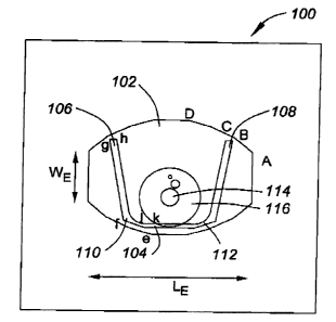
In FIG. 1, an antenna 100 is shown according to an embodiment of the present
invention including a polygonal shaped patch 102 having a modified V-slot. The
polygonal
-5
CA 02505433 2005-04-27
micrastrip patch and the modli9ed V-slot can be substantla~ly symmetrical with
respect to
a center axis perpendicular to the base of the microstrip patch, though such
symmetry i9
not required. The modified V-slot can be provided sub3tantially in the center
of the
polygonal microstrlp patch. ;
The polygonal patch shape and the modified V-slot co-operate to provide
current
shaping on the antenna. The muiGpficity of sides on the p~ygon shape provides
a higher
number of tunable parameters than the following shapes: riactangular;
circular; or a patch
having a generally rectangular shape but with two opposing sides having an arc
shape. A
dlamand shaped patch having eight straight sides can be implemented as the
polygonal
patch shape, with a patch having ten straight sides (or more) being a
presently preferred
implementation. The at least eight side segments are coriflgurabte with
respect to their
length andlor with respect to the angles between the side s~mertts.
Current shaping is performed in order to provide a sufficient current in one
direction. Current vector {or distribution) on a patch witHout a slot has
curr~nt in twp
directions; with the inclusion of the V-shaped slot, the curre~t i9 shaped so
that it is fn one
direction. Some known approaches have used a U-staaped slot on a rectangular
microstrip patch in order to attempt to provide a current vector in a single
din~ction.
However, the gain of antenna with a U-shaped slot is much tower compared to
the gain
provided aooording to embodiments at the present inverit'ron. Rectangular
microstrtp
patch antennas have been proposed including a V-slot. I~Uhile these antenna
elements
provide good perfom~ance in some respects, they are limited to use in wldeband
or
broadband applications, ;
The V-slot on the microstrip patch according to a~ embodiment of the present
invention includes a base segment 104 joined with two side segments: left V-
side
segment 108 and right V-side segment 108. The general shape of the throe
l~egments
resembles the shape of the letter "V", but being truncat~d at the bottom by
the base
segment 104.
With respect to the modified V-slot according to an smbodirnent of the present
invention, an extra element is provided as compare to known V-slot designs.
Embodiments of the present invention are provided for us~ in dual band, high
gain, high
frequency applications. With the limited number of parameters available in
known V-slot
patch antennas, it is not possible to split the bands in brder to be able to
vary the
performance of the antenna with respect to separate t7rands. In the modified V-
slot
acxording to an embodiment of the present invention, one dr more high
frequency control
segments are provided between the side segments 908 a~d 108 of the V and the
base
-6. I
CA 02505433 2005-04-27
104 of the tnrneated V. In FIG. 1, a left high frequency I segment 110 and
right
high frequency contrd segment 11Z ane provided.
The high frequency contrd segments 110 and ~ 12 provide control over the
frequency band in order to split the frequency band- The hi~h frequency
control segments
110 and 112 also provide a good linear polarization at hig~ frequency, good
gain at high
frequency, and a good input impedance matching at high fuency. As shown in
FIO. 1,
the left and right V side segments 106 and 108 can be proud at an obtuse angle
to the
left and right high-fre<iuency control segments 110 and 1~2, respectively, in
a dinaction
away from the base of the mtcrostrip patd~.
i
In an altematNe embodiment, additional high frequency control segments (not
shown) can be provided at the top of the two angled ses of the V, fn order to
provide
further tuning capabilities. In such an embodiment, the I antenna element can
further
include left and right additional high-hequency control segr~hents prrnrlded
at the open end
edge of the left and right V-side segments, respectively.
In other words, in an embodiment the present i wention provides a miCrostrip
patch antenna element including a convex polygonal mi~crostrlp patch having at
least
eight side segments configurable with respect to the perfortnan0e of the
antenna. The
patch has a modffied V-slot, a dosed end of the modi~ed V slot being
substantially
parallel to the length of the ba&e of the polygonal microstrlp patch. The
mpdlfled V-slot
includes a base segment defining the closed end, and le and right V side
configurable
segments each having a dosed end edge and an open d edge. The modified V-slot
also includes left and right high-frequency control segments configurable to
independently
control response of the antenna element in two irequency~ bends. The left and
right high
frequency control portions aro provided between and joini~g an end of the base
portion
and the do9~ed end edge of the left and right V-side portio s, respectively.
The polygor~l
mlcrastrip patch and the modified V-slot co-operate to pride high-frequency,
high~ain
dual-band operation-
The high frequency control segments 110 and 11?~ provide the ability to split
the
antenna response into two separate bands, or dual bans, and provides the
ablHty to
Independently control the response in those two bands In known wide band patch
antenna ~pplications, energy is radiated in areas which fare not of interest.
Also, the
tuning of the response is only available with respect to t ~ a twa ends of the
wide band
range and it is typically not possible to independently con the lower and
upper ends of
the wide band response- These drawbacks are overco according to embodiments of
the present invention.
CA 02505433 2005-04-27
As shown in FIG. 9, the left and right high frequ~ncy control segrnenta can be
provided at an obtuse angle to the end of the base porn I n in a direction
away from the
base of the polygonal miaostrip patch. The left and right h gh-frequency
control segments
can be configurable to independently control a first frequ nCy band lower
Ilmit and a first
frequency band upper limit, andlor a second frequency nd lower limit and a
second
frequency band upper limit.
The two frequency bands can comprise the Ku ba d and/or tha Ka band. The two
frequency bands in the dual band operation can indude a 1.5-12.75 GHz
reception band
and a 14-14.5 GHz transmission band.
The antenna element can further Include a fee ing point 114, such as a via,
provided substantially in the middk of the antenna el mart so that an offset
length
substantially equals zero, or any other oTfset length. antenna element can
further
include a probe, or aperture, 114 surrounding the fesdi g point and provided
generally
within a apace bounded by the portions of the modified V- lot.
Antennae according to an embodiment a~f the pre nt invendon can be used in an
Electromagnetic Band Gap (EBO) structure, where sk ants are provided around
the
antenna in a periodic manner. Such elements can include resonators. Another
optlan (s to
pr,ovlde a second patch on the same or on a different s strata layer, such as
above or
below a first patch. Providing a periodic structure aro nd the patch provides
a high
irnpedanoe around the patch at a particular fn~quency, p nts energy from
propagating
inside the substrata, and forces the energy to be transmi d outside the
substrate.
For tow frequency applications, it is often a cent to have a coarse current
shaping capability. With respect to high frequency epplice '~ls, a fine
control of the shape
is required in order to provide fine current shaping. Cu nt shaping with
respect to a
diamond shaped patch would generally entail adding an ther side to the patch.
With the
polygon shape according to an embodiment of the pre ant invention, there are
many
more parameters to be controlled. Fine tuning of thes parameters can result in
fine
shaping of the current pattern without requiring the ad ition of further
elements to the
patch, the behaviour of which may not be known.
The single and 4-element micxostrip polygonal sh pe patch with a modified V-
slot
on each element can be provided as a dual band linear p larlzed microstrip
antenna sub-
array. The antenna can work at 11.5-12.75 GHz for calving and 14-94.5 GHz for
transmitting mode; these ft'equency bandwidths are patible with FSS (Fixed
salute
system) Standard. Also this antenna can be incorporat in en array
configuration with
sequential feeding for DBS application.
-s-
CA 02505433 2005-04-27
Ar>bnna 4eometry
According to embodiments of the present invent n, the shape of the microstrip
patch is preferably provided as a polygon and a V slot is placed at the patch
center.
Alternatively, a diamond shapelarc can be used as the ch shape. In this
manner, with
a single-Payer patch, the impedance bandwidth of the p ch is Increased to
about 509'6
and it is possible to make dual band antenna for FSS end BS applicati~.
Referring again to FIG. 1, an exemplary geame of an antenna according to an
embodiment of the present invention is shown. The ant na is a single-layer
microatrlp
patch having a convex polygon shape and embedded m ified V-shaped slot. The
patch
main dimensions are Its length LE and width WE, and its sub-dimensions are
truncation
length I and w. The diamond or polygonal Shape of the pa ch increases its
length, thereby
exating its next higher-order mode, horizontal in FIG. 1. However, because of
the
reduction of patch width towards its end, the excitation f this higher-order
mode is not
very strong and the patch still radiates a strong vertlcall polarized field.
Consequently,
pladng this weakly exated mode between the patch do inant vertical mode and V-
slot
mode, inCneases the antenna bandwidth (and make it po Bible for dual band
application)
considerably. The antenna vertically polarized co-polar in remains high and
relatively
stable within the entire antenna impedance bandwidth.
Single element and 4-element modified V-sl t polygonal patch microstrip
antennas with a probe feed on the RTI Duroid d(eledri substrate are Shown in
FIG. 1
and FIG. 2, respectively. These elements are fad by xial probe or via to
maintain
linear polarisation for the antenna. The folded slot pare eters are optimized
to achieve
dual band Impedance matching for a given transmitting a receiving mode.
The geometry of the exemplary embodiment of the single antenna element in
FIG. 1 can be described by the following parameters: Su strafe : RTI Duroid
5880; ~
2.2; Tan d ' .0009; H=1.575 mm (82 mil). Polygon Shap : Ls = 11.2 mm ; Ws =
8.4 mm
A = (-.1 S, .5t3) ; B = (-.28, .47) ; C = (-.37, .28) ; D= (- 2,.1 ) ; LG ~ WG
= 20 mm. V
shape slot: LE = 11.2 rrun : WE= 8.4 mm ; a = (-.37, -.19 ; f = (-.28, ,47) ;
g = (-.28, -.42)
h= (-.28, -.32) ; i=(.28; .28) ; j=(.33,-.23) ; k=(,34,-.14).
The geometry of the exemplary embodiment of t four element (2x2) sub-array
in FIG. 2 can be described by the following parameters: ubstrate : RT/ Duroid
5880;
= 2.2; Tan d = .0009; H=1.575 mm (B2 mil). Polygon S ape: l.s = 11.2 mm ; WE=
8.4
mm;A=(1.191.86);B=(1.7.1.2);01=(1.16,1.1);D 1.14mm;D1=1.18mm;LG=
WO = 30 mm.
_g_
CA 02505433 2005-04-27
FIG. 3 Is a graph illustrating return losses for th antenna of FIG. 1 without
the
folded modified V-slot, with the remaining parameters bef g the same as FIG.
i_ t=IG. 4
is a graph illustrating return losses for the antenna of FI . 1 with the
folded modified V-
slot. A comparison of FIG. 3 and 4 demonstrates that the rovision of the
modified V-slot,
including the high-frequency control segments, provides dual bind performance.
FIGS.
3 and 4 represent variation of the r~etum loss versus equency for antenna with
and
without folded slot, with same polygonal patch shape. The antenna with folded
slot
bandwidth based on -10 dB return loss is from 11.4 G z to 12_5 OHz which
covers a
receiving mode frequency bandwidth.
FIG. 5 is a graph illustratjng antenna patfierns ( ~ 0 8~ rp = 90 ) at f~ =
11.7 GHz,
for the antenna of FIG. 1 without the folded modiB d V-slot, with the
remaining
parameters being the same as FIG. 1, FIO. 6 is a graph illustrating antenna
patterns ( cp
= 0 & cp = 90 ) at f, = 11.7 GHz for the antenna of FIG. 1. The antenna
maximum gain for
single element with and without folded slot are 7 d8i and .5 dBi, shrnm in
FIGS. 5 and 6,
respectively. FIG. 7 is a graph illustrating antenna pattern ( ~ = 0 & ~p = 90
) at f, =11.7
GHz for the 2 x2 sub array of FIG. Z. A 14 dt3i gain i available for the
configuration
described by FIG. 7.
Applications and Arrays
There arse two broad appllcatlons of antenna tches and arrays according to
embodimerds of the present invention. A linear polarizati n application is
advantageously
provided for use in intemet access transmission over sa Mite. Linear
polarization Is also
polarization is used for DBS
used in satellite DB5 transmission in Europe. Circuia
transmission.
A two by two black of antenna elements is the building block for any array of
elements. For intemet applications, some arrays that a used are two by four,
two by
eight, two by sixteen. In FIG. 2 an arrangement is hown for a linear
polarization
application.
Matching Network
FIG. 8 illustrates a top view of a V-slotted pat h antenna with matching and
feeding network according to an embodiment of the p ant invention- The
Impedance
Matching Network which IS shown in FIG. a is a novel wi eband design which
avoids the
effect of feed radiation on the antenna radiation patt m. Since the design
structure
separates patch antenna layer from feed network layer, a feed radiation is
blocked by
-10-
CA 02505433 2005-04-27
the ground plane of the design. The impedance of the en nna structure at the
center 120
of via-hole is Z,n~ ~"~, _ ?C + jY SZ based on the shape of used for the via-
hole. At the
edge 122 of via the Impedance is Z", ,~ = Xp ~ which has only a real part.
Using an
impedance transformer 124, such as a a/a impedance m thing network, this
impedance
is transformed to Xq ~ feed line 126- This structure sh very good matching
aver wide
frequency range.
In terms of mathematical relationships betw n the impedances, a N4
transfomner (quarter wavelength Ilne) with an imps nce of Z1 can match two
impedances of Z0, and 12 if Z1= S4RT(ZO'Z2).
As is shown in FIG. 8, the matching network port on around the via is cut off,
or
truncated, at the top of the circular portion. This cut off shape provides for
wide band
behaviour. In fact, the combination of the truncated rcular portion, the
impedance
transformer with a first width, and a further Impede ce line after the
impedance
transformer having a different width cooperate to provid wide band
pertormanoe. The
circular patdl with the portion of the circle cut off provide a particular
contribution to the
wide band perfom~anoe.
In other words, the present invention provides a Icrostrlp patch antenna
system
comprising a patch antenna layer having an antenna ale ant. Tf~e antenna
element can
be a mtcrostrip patch antenna element as described abov . The microstrip patch
antenna
system further indudes a dielectric layer having a via- , and a feeding and
matching
network layer having a wideband impedance matching k connected to the antenna
element by way of the via-hole. The matching netwo indudes a truncated
circular
segment having a first impedance, a feed line segment h ving a second
impedance, and
a transformer segment connected between the feed I ne segment end the
truncated
dn~ular segment opposite the truncated portion, !he tra sformer segment to
match the
first impedance and the second impedance.
Food Network
A feeding network of a module of 2x8 microstrip p tch antenna is shown in FIG.
9.
)n particular, FIG. 9 illustrates a Zx8 microstrip patch phased array antenna
feeding
network with 50-ohms matching netwofic at the output. A -slot 2x8 antenna
array with its
fe9ding network is shown in FIG. 10. tn particular, IG. 10 illustrates a 2x8 V-
Stot
rectangular microstrip patch phased array antenna ding network with 50-ohms
matching network at the output. The network is a T juncti n power combiner
concept that
adds power of 1t3 antenna elements and through a ~ impedance transformation
-11-
CA 02505433 2005-04-27
provides a SMA surface mounted connector output. Ea h T juncrfon power
oombiner
design is based on balance of power and phase combine ion of its inputs. The
de9ign is
not sensible to manufacturing tolerances and shows ve low insertion loss
across the
bandwidth.
The feed network can be provided as part of a eding and matching network
layer, as described earlier. In such a case, the feeding a d matching network
layer can
include a feeding network having a power combiner to mbine power of a
plurality of
antenna elements through an impedance transformatlo . The power combiner can
include a T junction power combiner based on balance of power and phase
combination
of its inputs.
Physics! Implementsfltlon
FIG. 11 illustrates a cross-sectional view of a patch ntenna structure
according to
an embodiment of the present invention. The structure f the antenna which
shown in
FIG. 11 comprises two high frequency substrates 150 and 152 bounded together
using a
bounding layer 154. The first high freQuency substrate 1 is a patch antenna
layer, and
the second high froquency substrate 152 is a feeding a matching network layer.
The
bounding layer 164 can be an FR4 bounding layer with .5 mils thickness, b.5
relative
dielectric constant and 0.018 k>,ss-tangent. A top lamina , or layer, 156 is
provided as
part of the mufti-layer board, and can be I~ogars RTIDuroi 5880 with 82 mils
thfdcness,
2.2 relative dielectric constant, 0.0009 loss-tangent an 1 ounce copper. A
bottom
laminate, or layer, 158 can be Rogers 803003 with 20 mil thickness, 3 relative
dielectric
constant, 0-0013 loss-tangent and 1 ounce copper. The p tch antenna is
provided In the
patch antenna layer 150, provided at the top layer 1 . The feeding and
matching
networks are provided in the feeding and matching netw rk layer 152, provided
at the
bottom layer 198. A via-hole 160 is provided In this em diment to perf~m
connection
between the lw~o layers, or substrates. The bottom layer 1 serves as the
ground for the
board. The slot on the ground surface avoids connection o via-hole to the
ground and its
diameter is preferably optimized to have maximum effcien for the antenna.
Thermal coefficients of substrates can be -125 and 1 S ppml°C fa top
and bottom
laminates, respectively. Because of different thickness for the layers and
different
composites (glass reinforced PTFE for the top layer an ceramic ~118d PTFE for
the
bottom layer), during the bounding process, no significant warping is
generated. So this
antenna design is manufacturable and the via-hole is not s sceptible cracking
upon wide
temperature variation.
-12-
CA 02505433 2005-04-27
Asymmehical Antenna Array
FIG. 12 shows an array 170 of mlcrostripaccording
anten to
an
embodiment
of the present invention. The array r
of FI(3. 12 is for circu polarization
suitable
for
DBS
application. Typically, a 2x2 array s must include four
of antenna elemen identical
antenna elements. Embodiments of provide
the present invention an
asymmetrical
array
of microstrlp antennas. Each of the elements
micrastrip antenn has
a
plurality
of
configurable elements or segments, I
such as the polyp patch
with
modlfled
V-slot
descxfbed earlier. This arrangement of
gives a higher degre freedom
to
allow
for
small
perturbations to occur end still
have optimised performan
In the embodiment shown In FIG. 1Z, y
a 2x2 ar of
four
microstrip
antenna
elements is provided. First and seconda elements 1T2 and
microstrip anten 174 are
provided diagonally opposite each latly similar to
other, and are substa f each other. In
stating that the first and second elements
microstrip antenna 972
and
174
are
substantially similar tp each other,invents
this includes emb wherein
they
can
be
identical, or can nary with respect .
to small perturbs ' Third
and
fourth
microstrip
antenna elements 176 and 1T8 are poslte each other
provided diagonally o as well, and
are substantially similar to each rostrip antenna
other. The first pair of mi elements (172
and 9T4) are not similar to the secondenna
pair of microsttip a elements
(170
and
178).
Of course, this example is only one embodiment,
embodiment. In ono each
of
the
four
mia~ostrip antenna elements can be rs
different fnxn the oth with
no
substantial
similarity
among them. Since each of the microstripelements
antenna has
a
plurality
of
configurable sections or parameters,be
those parameters conflgurodltuned
in
order
to provide a desired overall performance,imifar
even with di elements
in
the
same
array.
In the configurat(on of FIG. 12, patches
diagonally opposi are
similar
in
shape
but different from those patches ther embodiment,
of another diagonal. In an the polygon
shape of each microstrip patch in n
the 2x2 configuration be
different
from
each
o#~er
to minimize the mutual effect betweenthe
patches and increas gain.
An asymmetrical micrastrip patch is
antenna arra not
limited
to
examples
discussed herein. For example, such in
a patch configursti 2x2
array
can
be
provided
for Circular polarization or for
linear polarization.
In other words, an asymmeMcal array ntennas
of microstrip is
provided
including
four rnicrostrip patch antenna elementssquare
arranged in configuration.
Each
microstrlp patch antenna element gurable
has a plurality of elements.
Diagonally
opposite patches are substantially afferent
similar in shape but in
shape
from
those
patches of another diagonal.
-13-
CA 02505433 2005-04-27
The four mic~ostrip patch antenna elements n include: first and second
micxostrip patch antenna elements being substantially sl lar to each other in
shape arid
performance and provided diagonally opposite one a other; and third and fourth
microstrip patch antenna elements being substantially sim lar to each other in
shape and
performance and provided diagonally opposite one a other. The third and fourth
micrastrip patch antennas are dissimilar from the first and second microstrip
patch
antenna elements. The first, second, thud and fourth mi trip patch antenna
elements
can each have at least eight configurable patch segments. The substantially
similar pairs
of elements can be rotated in phase with respect to each o er.
The first, second, third and fourth mlcrostrlp patch ntenna elements can each
be
a convex polygonal microstrip patch having at least eight s a segments
configurable with
respect to the pertormance of the antenna. The patch n have a modtned V-slot,
a
dosed end of the modified V slot being substantially petal to the length of
the base of
the polygonal miCrostrip patch. The modified V-slot can i ude: a base segment
deftning
the doaad end; left and right V-side configurable segme is each having a dosed
erxi
edge and an open end edge; and left and right hig frequency control segments
configurable to independently control response of the ante na element in two
frequency
bands. The left and right high frequency control portions provided between and
join
an end of the base portion and the dosed end edge of the left and right V-side
portions,
respectively. The polygonal micxostrip patch and the rnodifi V-slot co-operate
to provide
high-frequency, high-gain dual-band operation.
System implementation
Reflector antennas with rather high gain are necess ry for reception of
signals for
Ku band satellite cammunicatiort. However, they cannot tie sad on moving
platform such
as cars and buses because of restriction on dimensions and aerodynamics.
Relatively flat
antennas are desirable for this type of applications.
Two examples of such a low profrle antennas h a been reported for digital
broadcast satellite reception to cover South Korea and Jap n. However, because
these
two countries are relatively small, scanning at elevation was not an important
concern. In
Current ressearch situation the coverage area is as large as, ndnental United
States and
Ganada. This generally requires increase in the 9aln and ale tion annular
range at same
time which aro the conflicting requirements as the incre se of antenna
longitudinal
dimension requin:d for high gain, could generally lead to de ease in the beam
scanning
range.
-14-
CA 02505433 2005-04-27
A practical sdutfon to this problem by using hybrid
can be found phased array
antenna with both electronic and g.
mechanical beam acann The
satellite
tracking
in
this
system uses mechanical scanning in on far the coarse
azimuth and elevat tuning. The
electronic beam steering is used tion
for both azimuth and ale scanning,
fine-tuning
and
compensation for the road condition.educe
This method will the
number
active
and
control elements while maintaining
the high performance.
The system described here is a low configuration
profile syste for
any
phased
array antenna systems for mobile )
(vehicular applicatio or
stationary
reception
and
transmission of signal through s8tellite.ication
The special ap is
Ku,
Ka
band
,
land
mobile DBS (Dined t~adcasting satellite)
and Internet.
Low profile is one of the important Therefore,
specifications. a
stair-planar
array
structure is preferably provided, ich
as shown in FIG. 13, in a
large
antenna
Is
divided
into a series of sub-an~ys 1$4 locatedher.
in parallel to each The
height
of
the
panels,
on which the sub-arrays are preferablybly
provided, is profe equal,
though
this
is
not
a
necessary condition. The length of r equal or non equal
each panel can be eith as shown
in FIG. 14. The panels are located do
in such a way that the not
block
each
other
for
all
elevation scan angles. The panels eChanical
can rotate through a joint
from
20
to
7t7
degrees in the y-z plane. All panelsrotating plate 182,
are mounted on a which can
rotate In the x-y plane more than s
3B0 degrees with the z-a to
be
the
axis
of
rotation.
The rays coming from a satellite wave
travel in plane formation.
The
first
ray
arrives at the panel 1 first then an
the second ray after travail extra
distance
DL
gets
to
p8r~ei 2 and so on till the n ray xtra
reach to panel n travel an disklnCe
of
(n-1
)
DL.
This
situation causes the phase en-or treatments
between the panels. T using
RF
cable
length oompensatlon (as shown in er
FIG.15) and phase sh compensation
are
applied.
We consider the RF cable length cooner
in o to
treat
a
multl-planar
array
as a whole planar array. The requiredconnecting
Li of each coaxial between
sub-~erray
and phase snifter is L, = Lo + (n - i)nL I ~ , where L-0 ~S the minimum
length, E to a
permittivity of coaxial cable oL' = dL / ~ and DL is en av~tage distance
between panels
when the panels rotate in elevation plane (hero 20 to 70 degree). After the
phase
adjustment by the cable, the signal enters the phase shifts for fine phase
adjustment and
then combined by power combiner.
Trads;ing specifications of an ultra low profile based array antenna system
according to an embodiment of the present invention will ow be described. The
system
can comprise multi panel antenna arrays arranged in o groups: left hand
circular
polarization (LHCP) group and right hand circular polarize n group (RHGP).
Each group
-15-
CA 02505433 2005-04-27
has its own radiation pattern. So the system would have o radiation patterns.
FIG. 18
illustrates a 10-panel ultra low profile phased array syste aCOOrding to an
embodiment
of the present invention with its associated LHCP and RH radiation patterns,
otherwise
described as dual polarization radiation patterns.
Both radiation patterns 1 tint and 1 BB are almost a same: they are relatively
nanow in azimuth direction and wide in elevation direction nd side lobes
levels aro much
suppressed however grating lobes exist.
In an attemative embodiment, instead of having two differently polarized
groups pf
mull panel antenna arrays in the same antenna system, plurality of systems can
be
provided for use with each other, with each system having ifferently polarized
groups of
multi panel antenna arrays. Each separate ultra low pro le antenna system can
then
logically be considered to be a sub-system of the larger sy em. These sub-
systems can
preferably be provided in pairs, such that an over-archi system Can include a
dual
configuration, or a four sub-system configuration, etc.
FiG. 17 is a block diagram of an ultra low profile based array antenna system
Z00 according to an embodiment of the present invention As shown in FIG. 17,
each
pane! 20Z of tile 10-panes system comprises severe! modul s which each module
has its
own LNA 204. The exemplary system in FIG. 17 has 97 uses for each
polarization.
The outputs of all module-LNA pairs for each polarization g up are oonneGted
to a 17-to-
1 phase shifter / power combiner board (PS-PC). LHCP S-PC board 206 and FtHCP
PS-PC board 208 are controlled by a Control Board 210.
in FIG. 97, tire control board 1i0 also controls two r driver boards Z12
driving
two stepper motors 214. Both outputs of PS PC boar~da go an LNB 216 which
provides
outputs for SateAlte receivers. FIG. 18 is a perspective view f an ultra low
profile phased
amdy antenna system according to an embodiment of the p sent invention.
System tracking design is based an controlling pha shifters and stepper motors
simultaneously. So the system is able to lock to the satellite and track It
both
mechanically aid electronically. This specification impro drastically the
tracdng
performance of the system and gives a huge advantage to it.
System Specifirca#on
Since the system has very law height, its radiation b am becomes very narrow
in
azimuth direction and because of the nature of the appli tion, which Es the
mobile
satetlits terminal. Tracking performance in azimuth direction comes important.
For normal low profile mobile satellite terrninais, the am width of the system
in
the azimuth direction is about 3-V4 degrees. This beam width enough to be able
to track
_ig_
CA 02505433 2005-04-27
the satellite in almost every road Conditions and driving kills, However, in
the case of
ultra low profile systems, which includes our system, t a beam width in the
a~Jmuth
direction becomes very narrow. For our system, the aximu beam width is in the
range of
0.5--0.7 degrees. Such a beam width makes the cyst m very sensible to azimuth
movements and fluctuations. One of the masons for an ul a low profile system
being so
competitive in the market la this ultra narrow azimuth beam width.
Embodiments of the pra5ent irwentian overcome the s~nsltivity to the aamuth
vibrations and noises by making the beam to tae able to steered electronically
in the
azimuth direction. The system also has the advantage of Iectronlc beam
steering in the
elevation direction as well. in the following section we describe the tracking
specifications of the system.
Mechanical beam steering In elevatNM dkeCtion
The ultra low profile phased array antenna system s able to lode on and to
track
the satellite everywhere in the North America continent. Thi capability is
achieved thanks
to the innovative mechanical design of the system. The pa els of the System
are able to
have a tilt angle varying from 20 degrees to TO degrees ran . This range, when
added to
the electronic beam steering capability of the system, mak the system able to
lock and
tracfc the sat~Ilite everywhere from Alaska toward Florida pl s some parts of
Mexico.
FIG. 19 Illustrates mechanical beam steering in an levatlon direction of an
ultra
low profile phased array antenna system according to a embodiment of the
present
invention. In the figure dual beams 2Z0 and ~2 are scanni g in the elevation
direction in
big steps to show how the beam will steer in that direction, owever, in
practice the pace
of the steps is much smaller and almost a continues scanni is provided.
For each panel's tih angle, a specific phase difieren between successive
panels
should be applied to have the beam perpendicular to the pa els. The lpok-up
table in the
tracking algorithm will provide the required data to put the pa els in phase.
Mechanical Beam Steering of the System
In Azimuth Dlrecti
FIG. ZO r~lustrates mechanical beam zimuth direction
steering in an of an ultra
low profrle phased array antenna systemembodiment of
according to an the present
invention. The beam 22d scans in the
azimuth dinectlon.
Since the application of the system mobile users,
is intended f the system
should be able to scan the azimuth 3t30 degrees.
angle from 0 degrees t The azmuth
step-motor makes the system fully rotatingirection and the
in the azimuth rotary joint
. 17 .
CA 02505433 2005-04-27
technique solves the signal transmission problem from t a rotating platfomt to
the fix
platform_
The resolution of the steps In the azimuth direction i very high. With a step-
motor
of 52000 steps for single rotation, a resolution of leas than .01 degrees can
be obtained,
which is sufficient fpr high precision mechanics) 8dj stment. In some
practical
implementations, a resolution of 0.2 degrees for the sy tam may be obtained.
This
number is still avoeptrable thanks to the electronic beam st ertng which
offers fine tuning
role in this case.
Electna~nic Seem ~eerrng of the System
The system is able to steer its beam both
etectronira!!y I azimuth
and
elevation
direc~ons. Since in electronic beam for
steering there is na nee mechanical
movements,
the stesrfng speed is much faster eering.
than mechanical beam By
proper
design
of
the control boards and minimi~ng the pC
delays for DAC and boards,
it
is
possible
to
achieve an electronic beam steering . The range of
speed of above 10 KH steering angle
in azimuth direction is t3 degrees. th
That means beam in
azimuth
according
to
embodiments of the present invention a
can be Interpreted degrees
which
is
enough
far overcoming substantially all vibrationszimuth
and noises in the direction.
Beam steering range in elevation directiont5
Is abo degrees.
This
coverage
range is important to avoid mechanicalelevation
beam steering In th direction
for
most
of the tracking scenarios, t?nly for at
long traveling distances produce
btg
changes
in
elevation angles of the system with ill
respect to the satellite, cause
mechanical
beam
steering in the elovatton direction. the
This epeclflcation enable system
to
provide
very
long lifetime because the cabling anels
and connections of the are
not
moving
very
much.
FIG. 21 shows a range of electronic beam steeling the azimuth arid elevation
directions_ An azimuth electronic beam steerYng range 226 and an elevation
electronic
beam steering range ?,28 are shown. Depending on the re lotion of the DAC
board to
Control the phases of the phase shifters, the resohrtion of t electronic beam
steering
could be very high and In the range of thousandths of d grees_ FIG. 22 shows
the
steered beam at four extreme angles of the CovBn~ge range and its initial
position in the
center of the range. An electronic beam steering range Z30 ' shown.
Method of Tracking
In order to point the antennae at the desired satellite position while the
vehicle is
moving, the antenna controller (preferably embodied in a microprocessor)
steers the
_16_
CA 02505433 2005-04-27
antenna beam electronically in both azimuth and eleva ion angle in response to
RF
detector to achieve motion compensat(on. The referred embodtment uses
accelerometers and yaw, roil, and pitch sensors to se se the yaw, pitch, roll
rates,
longitudinal and lateral aooeietatton of the vehicle and PS and C3yro. The
estimated
yaw, roll and pitch rates are integrated to yield tire vehlde w, pitch, and
roll angle. This
is used in a coordination transformatbn to the earth-axed ordinate system to
determine
the azimuth and elevation travel of the antenna. The ntenna will be fumed in
the
opposite directions by the same amount to counteract th vehicle motion. My
resulting
pointing error Is detected by a dithering process and co d by the antenna
traddng
system. Drill due to the inertia bias is the mast significant roe of pointing
error and the
tradting system compensates for it with dithering.
According to the antenna tracking algorithm, the tenna beam electronically fs
dithered to the lest, right, up, and down of the target by s certain amount.
The received
signal strength indicator (RF detector) is monitored d ring dtls dithering
action to
determine the pointing error pf the antenna beam. The ant nna pointing is then
adjusted
toward the direction of maximum signal strength to refine th antennae
tracking.
According to a preferred embodimernt of the inv ntion, the antenna caantrolter
obtains an estimate of the pointing angle error by "ele icaliy dithering" the
antenna
position. Electronic dithering in the elevatMn and azimu diredlon are achieved
by
changing (incrementing or decrementing) the phase ahi of the phase shifters by
a
certain amount. This is equivalent to moving the antenna m (upward or downward
left
and right) in elevation and azimuth_
The advantage of the "electronic dithering" is that a power required is
reduced
as compared to that required for constantly mechanlca(ly dit ring the antenna
assembly.
A send advantage is that the "electronic dithertng" Can performed at a much
faster
speed than the "mechanical dithering". Fast dithering ope lion means the
antenna can
trade faster, which can eliminate the need for motion Compensation and all the
components (accelerometers and pitch, and yaw sen ) repaired by the motion
compensation, resulting In a sign'rficantly lower cost imptem tation.
When the antenna assembly is first powered up, a controller mi
croprocessor
whid~ controls the azimuth and eievativn motors and comm nds the two motors to
move
and monitors the encoders to check if the two motors respo to the command.
After that,
the motion Compensation algorithm is fumed on. The a tennae are moved to scan
through possible satellite positions to search for a satellite si nal. The
typical method is to
scan the 360 degroe azimuth angle at a 9ivsn elevatio , incrementally change
the
elevation angle, and repeat the azimuth scan. Preferably, a electronic compass
or aPS
- t9 -
CA 02505433 2005-04-27
is utilized and the location of the satellite is known. Thus, r will not be
necessary to scan
the enttte hemisphere, but only a relatively smelt region ased on the accuracy
of the
compass and the satellite position. The antennae dither a 'on is not turned an
during the
initial satellite lorx3tion. The antennae controller monitors a RF detector
via the power
monitor. If the power monitor detects that the signal streng exceeds a certain
threshold,
the scanning is stopped immediabaly and the antennae dl ring algorithm is
turned on to
allow the antennae to trade the ai9nal. The demodula (receiver) and the data
processor are monitored to see if the antennae are points at the desired
satellite and if
the signal Is properly decoded. If that Is the case, the sign I lode is
achieved. Otherwise,
the antenna dithering is disabled and the scanning Is resum
If the signal lock is achieved, the antenna tracking algorithm continues to
retina
the antenna tracking. The processor which controls th motors and phase
shifters
continues to report the motor position with a time tag. In t proferred
embodiment, the
motor position is translated into a satellite position (elevati n and azimuth)
in space. In
the case that the signal is blocked by trees, buildings, other obstacles, the
power
monitor and the reoehre data processor can immediately elect the loss of
signal. The
antenna tracking algorithm will command the motor cont Iler and DAC to move
the
antenna back to point at the last satellite position recorded, when the
satellite signal was
property decoded- In addition, upon loss of signal, th antenna dithering
tracking
algorithm wilt be temporarily turned o~_ tf the power moni r detects the
signal power
(exceeding some threshold) again or the data provessor de s the signal lo!dc
again, the
antenna dithering algorithm will be fumed on again to con rue tracking. After
a certain
time-out period if no signal atr~ength exceeding the thresh 1d is detected by
the power
monitor a the data processor does not detect signal ixk, th antenna scanning
algorithm
will be initiated to scan for signal again. The antenna-sea ring algorithm for
signal re-
aoquisltion wilt scan in a limited region around the last sa life position
riecorded, when
the satellite signal was prop$rly decoded. tf the scanning do s not find the
satellite signal,
a full scan of 360 degrees of azimuth angle aril all possl to elevation angles
will be
conducted.
As mentioned earlier, an antenna according to an mbadiment of the present
invention can be provided in a P8G structure. A mufti-lays antenna (stacked
antenna)
can be provided in which at least one antenna Is an antenna cxording to an
embodiment
of the present invention. An array can be provided with two pairs of
dissimilar antennas
according to an embodiment of the present invention. A antenna according to an
embodiment of the present invention can be used for bBS or Internet
application through
-20-
CA 02505433 2005-04-27
satellite. An antenna accordin~ to an embodiment of the pre ent Invention can
be used as
an array with any form of feed configuration to generate line r or Circular
polarization.
The above-described embodiments of the present nvention are intended to be
examples only. Alterations, modifications and variations ma be effected to the
parracutar
embodiments by those of skill in the art without departing f the scope of the
invention,
which is defined Solely by the claims appended hereto.
-21 -