Note: Descriptions are shown in the official language in which they were submitted.
CA 02505482 2005-05-06
WO 2005/038983 PCT/US2004/027440
DIRECTIONAL ANTENNA ARRAY
TECHNICAL FIELD
[0001] The present invention generally relates to an antenna, and more
particularly relates
to a directional antenna array.
BACKGROUND
[0002] Yagi-Uda antennas were originally described in the English language in
an article
written by H. Yagi (See H. Yagi, "Beam Transmission of the Ultra Short Waves,"
Proc.
IRE. Vol. 16, pp. 715-741, June 1928). These directional dipole antennas,
which are
commonly referred to as Yagi antennas, have been used for many years and in
many
applications. For example, the Yagi antenna has been used for reception of
television
signals, point-to-point communications and other electronics applications.
[0003] The basic Yagi antenna typically includes a driven element, usually a
half wave
dipole, which is driven from a source of electromagnetic energy or drives a
sink of
electromagnetic energy. The antenna also typically includes non-driven or
parasitic
elements that are arrayed with the driven element. These non-driven or
parasitic elements
generally comprise a reflector element on one side of the driven element and
at least one
director element on the other side of the driven element (i.e., the driven
element is
interposed between the reflector element and the director element). The driven
element,
reflector element and director element are usually positioned in a spaced
relationship along
an antenna axis with the director element or elements extending in a
transmission or
reception direction from the driven element. The length of the driven,
reflector and director
elements and the separations between these antenna elements specify the
maximum
Effective Isotropic Radiated Power (EIRP) of the antenna system (i.e.,
directive gain) in the
antenna system's bore site direction.
[0004] Current trends in antenna designs reflect the desirability of low
profile, directional
antenna configurations that can conform to any number of shapes for a mobile
or portable
unit while providing highly directional antenna patterns, such as those
achievable with the
Yagi antenna. In addition, current trends in antenna designs reflect the
desirability of the
CA 02505482 2005-05-06
WO 2005/038983 PCT/US2004/027440
antenna to maintain structural shape and integrity after application of an
external force, such
as a surface impact. Such antenna designs are particularly desirable in
portable or hand-held
devices such as cellular telephones, satellite telephones and contactless
interrogators of
Automatic Identification (Auto ID) systems, such as Radio Frequency
Identification (RFID)
interrogators of RFID systems.
[0005] Accordingly, it is desirable to provide a low profile, directional
antenna that can
conform to any number of shapes while providing highly directional antenna
patterns. In
addition, it is desirable to provide an antenna that can maintain structural
shape and integrity
after application of an external force. Furthermore, it is desirable to
provide such an
antenna for portable or hand-held devices. Moreover, desirable features and
characteristics
of the present invention will become apparent from the subsequent detailed
description and
the appended claims, taken in conjunction with the accompanying drawings and
the
foregoing technical field and background.
BRIEF SUMMARY
[0006) A directional array antenna is provided in accordance with a first
exemplary
embodiment of the present invention. The directional array antenna comprises a
driven
element and a first parasitic element separated from the driven element. The
first parasitic
element and/or the driven element has a width that is preferably greater than
about one-half
a percent (0.5%) of an free-space wavelength of the directional antenna array.
[0007] Alternatively or in conjunction with the first exemplary embodiment, a
directional
array antenna is provided in accordance with a second exemplary embodiment.
The
directional antenna array includes a balun structure that is configured to
couple the driven
element to at least one of an electromagnetic energy source and an
electromagnetic sink, and
the balun structure includes a dipole structure, a first feed point extending
from the dipole
structure and a second feed point extending from the first parasitic element.
2
CA 02505482 2005-05-06
WO 2005/038983 PCT/US2004/027440
BRIEF DESCRIPTION OF THE DRAWINGS
[0008] The present invention will hereinafter be described in conjunction with
the
following drawing figures, wherein like numerals denote like elements, and:
[0009] FIG. 1 a planar view of the directional array antenna in accordance
with an
exemplary embodiment of the present invention;
[0010] FIG. 2 is a planar view of the directional array anteima with parasitic
elements in
addition to the parasitic elements illustrated in FIG. 1;
[0011] FIG. 3 is a first example of a non-planar folded configuration of the
directional
array antenna of FIG. 1 in accordance with an exemplary embodiment of the
present
invention;
[0012] FIG. 4 is a second example of a non-planar folded configuration of the
directional
array antenna of FIG. 1 in accordance with an exemplary embodiment of the
present
invention;
[0013] FIG. 5 is a balun structure for the directional antenna array of FIG. 1
in accordance
with an exemplary embodiment of the present invention;
[0014] FIG. 6 is the directional array antenna of FIG. 3 with an elastomer
cover in
accordance with an exemplary embodiment of the present invention;
[0015] FIG. 7 is the directional array antenna of FIG. 1 with apertures; and
[0016] FIG. 8 is a portable/handheld device having the directional antenna
array of FIG. 6
in accordance with an exemplary embodiment of the present invention.
DETAILED DESCRIPTION
[0017] The following detailed description is merely exemplary in nature and is
not
intended to limit the invention or the application and uses of the invention.
Furthermore,
there is no intention to be bound by any expressed or implied theory presented
in the
preceding technical field, background, brief summary or the following detailed
description.
3
CA 02505482 2005-05-06
WO 2005/038983 PCT/US2004/027440
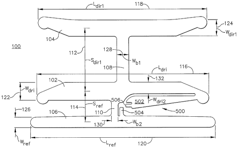
[0018] Referring to FIG. 1, a planar view of a directional antenna array 100
is provided in
accordance with an exemplary embodiment of the present invention. Generally,
the
directional antenna array 100 includes a driven element 102 and at least one
(1) parasitic
element or director element 104, and preferably a second parasitic element or
reflector
element 106 in addition to the director element 104. While only two parasitic
elements (i.e.,
director element 104 and reflector element 106) are shown in FIG. 1 in
addition to the
driven element 102, any number of parasitic elements can be provided in
accordance with
an exemplary embodiment of the present invention. For example, a directional
antenna
array 200 is shown in FIG. 2 with four additional (4) parasitic elements (202,
204,206,208),
which can be one or more additional director or reflector elements in addition
to the director
element 104 and reflector element 106 as shown in FIG. 1. Alternatively, the
directional
antenna array 100 can consist of (i.e., has no more or no less): a driven
element and a
reflector element; a driven element and a director element; a driven element
and multiple
reflectors, a driven element and multiple directors, or a driven element with
a combination
of one or more director elements and reflector elements. In addition, these
one or more
additional director or reflector elements can be in-plane elements or out-of
plane elements,
such as a trigonal reflector system having a first reflector positioned above
and a second
reflector positioned below a third reflector.
[0019] With continuing reference to FIG. 1, the driven element 102 is
preferably the
equivalent of a center-fed, half wave dipole antenna. The director element 104
is positioned
on one side of the driven element 102 and connected with a boom 108 and the
reflector
element 106 is preferably positioned on the other side of the director element
102 and
connected with another boom 110 such that the driven element 102 is interposed
between
the director element 104 and the reflector element 106. In addition, the
director element 102
and the reflector element 106 are positioned in at least a substantially
parallel relationship
with respect to the driven element 102 and more preferably a parallel
relationship with
respect to the driven element 102.
[0020] In this exemplary embodiment, the directional antenna array 100 is a
Yagi antenna.
Accordingly, as known to those of ordinary skill in the art, the design of the
directional
antenna array 100 involves selection of parameters of the driven element 102,
director
element 104 and/or reflector element 106 and other parameters of additional
parasitic
elements of the directional antenna array 100 is such elements exist. For
example, the
design of the directional antenna array can include selection of spacing
between the
4
CA 02505482 2005-05-06
WO 2005/038983 PCT/US2004/027440
elements (e.g., spacing (Sdirl) 112 between the driven element 102 and the
director element
104 and spacing (Sref) 114 between the driven element 102 and the reflector
element 106),
element lengths (e.g., driven element length (Ldr;) 116, director element
length (Ldirl) 118
and reflector element length (Lref)120), element widths, which as used herein
shall include
element diameters (e.g., driven element width (Wdr; )122, director element
width (Wdirl) 124
and reflector element width (Wref ) 126). However, other parameters and
parameters of
additional antenna structures) can be used in the design of the directional
antenna array 100
in accordance with techniques known to those of ordinary skill in the art
(e.g., boom widths
(Wbl) 128, (Wb2) 130).
[0021] In accordance with an exemplary embodiment of the present invention, at
least a
portion of one of the driven element width (Wdri) 122, director element width
(Wa;ri) 124
and reflector element width (Wref) 126 is greater than about one-half a
percent (0.5%) of a
free-space wavelength of an operating frequency of the directional antenna
array 100, which
shall be referred which shall be referred to herein as the free-space
wavelength, and
preferably the free-space wavelength of the center frequency of the
directional antenna array
100. Preferably, at least a portion of one of the driven element width (Wdri)
122, director
element width (Wd,u) 124 and reflector element width (Wref) 126 is greater
than about one
percent (1%) of the free-space wavelength of the directional antenna array
100. More
preferably, at least a portion of one of the driven element width (Wdri) 122,
director element
width (Wdirl) 124 and reflector element width (Wref) 126 is greater than about
two percent
(2%), and most preferably greater than about four percent (4%). The driven
element 102 is
preferably the element with a portion having the width (i.e., Wdri 122) that
is greater than
about one-half a percent (0.5%) of the free-space wavelength of the
directional antenna
array 100, preferably greater than about one percent (1%) of the free-space
wavelength,
more preferably greater than about two percent (2%) and most preferably
greater than about
four percent (4%).
[0022] In addition to at least a portion of one of the driven element 102,
director element
104 and reflector element 106 having the width relationship to the free-space
wavelength as
previously described in this detailed description, the element shapes (i.e.,
round, square,
triangular, pentagonal, hexagonal, etc.), the driven element length (Ldri)
116, the reflector
element length (Lref) 120, the director element length (Ldir) 118, the
director element spacing
(Sdirl) 112 and the reflector element spacing (Sref) 114 are selected in
accordance with the
electrical resonant frequencies of the elements in accordance with techniques
known to
CA 02505482 2005-05-06
WO 2005/038983 PCT/US2004/027440
those of ordinary skill in the art. For example, the parameters of the
directional antenna
array 100 are selected such that the electrical frequency of resonance of the
director element
104 is preferably greater than the free-space wavelength and the electrical
frequency of
resonance of the reflector element 106 is less than the free-space wavelength.
[0023] As known to those of ordinary skill in the art, any number of design
variations
exists for the directional antenna array (i.e., Yagi antenna) with the width
relationship to the
free-space wavelength in accordance with an exemplary embodiment of the
present
invention. For example, preferred boom width (Wbl) 128 and length and spacing
of the
driven element 102, director element 104 and reflector element 106 for a
frequency range of
approximately nine hundred and two megahertz (902 MHz) to about nine hundred
and
twenty-eight megahertz (928 MHz) is provided in Table 1.
Table 1
Driven Director Reflector
Width 0.56 inches 0.49 inches 0.33 inches
%Width 4.35% 3.8% 2.57/~
Spacing 0.89 inches 2.75 inches 0.89 inches
%Spacing Not applicable 14.4% 6.9%
Length 5.19 inches 5.04 inches 5.60 inches
Length 40.2% 39% inches 43.4%
Where %Width, %Spacing and %Length are percentages of the free space
wavelength and
director spacing is the spacing (Sd;u) 112 between the driven element 102 and
the director
element 104 and the reflector spacing is the spacing (Sref) 114 between the
driven element
102 and the reflector element 106.
[0024] In accordance with an exemplary embodiment of the present invention,
the
illustrative example presented in Table 1, and other directional antenna
arrays designed in
accordance with the present invention, is preferably formed of a monolithic
material having
a thickness that is greater than about one skin depth at an operating
frequency of the
directional antenna array 100. The monolithic material can be any number of
materials such
as spring steel, beryllium copper, stainless steel or a combination thereof,
and the monolithic
material preferably can have a resistivity that is greater than about 0.1 x 10-
6 ohms-meter,
preferably a resistivity that is greater than 0.2 x 10⁻⁶ ohms-meter, more
preferably greater
than 0.4 x 10⁻⁶ ohms-meter, even more preferably greater than 0.8 x 10⁻⁶ ohms-
meter, and
most preferably greater than 1.0 x 10⁻⁶ ohms-meter and 2.0 x 10⁻⁶ ohms-meter.
For
example, the directional antenna array with the dimensions illustratively
presented in Table
6
CA 02505482 2005-05-06
WO 2005/038983 PCT/US2004/027440
1 can be formed with a thickness of about one-sixteenth (1/16) inch FR-10 P.C.
Board
(PCB) and a two thousandths (0.002) inch copper tape formed on at least one
side of the
PCB.
[0025] With the directional antenna array 100 stamped, laser cut, water jet
cut, or
otherwise formed from the monolithic material, the driven element 102 is
preferably formed
into a non-planar folded configuration. For example, the distal ends (302,304)
of the driven
element 102 are folded to provide an angle of about ninety degrees
(90°) with respect to the
boom 108 to form the non-planar folded configuration 300 as shown in FIG. 3.
Alternatively, and by way of example only, another non-planar configuration
400 can be
formed by continuing to fold the distal ends (302,304) of the driven element
102 until such
ends are substantially adjacent and preferably directly under the boom 108 as
shown in FIG.
4 or folded into any number of other shapes other than the elliptical shape of
FIG. 4 (circle,
square, triangle, etc). Furthermore, the director element 102 and/or reflector
element 104
can be folded in a manner that is similar or the same as the driven element as
shown in FIG.
3, in a different manner that is not similar to the driven element as shown in
FIG. 4, or in
any other manner to provide specific antenna characteristics or antenna
aesthetics.
[0026] Referring to FIG. l, the driven element 102 is preferably coupled to a
source of
electromagnetic energy (not shown) and/or coupled to a sink of electromagnetic
energy (not
shown). The directional antenna array 100 of the present invention is
inherently a balanced
antenna, and the directional antenna array 100 is preferably coupled to the
source and/or
sink of electromagnetic energy to an unbalanced connector (e.g., a coaxial
transmission line
(not shown)) using a balun or baluning structure 500. The balun structure 500
is preferably
configured for impedance-matched Radio Frequency (RF) energy to flow in either
direction
within the coaxial transmission line without the introduction of RF energy
onto the outside
of the coaxial transmission line. As can be appreciated, RF energy flowing on
the outside of
the coaxial transmission line is inherently wasteful and generally distorts
the directive
pattern of the directional antenna array, thus lowering the maximum bore sight
gain.
[0027] Refernng to FIG. 5, an enlarged view of the driven element 102 is shown
that
presents an exemplary embodiment of the balun structure 500 in accordance with
an
exemplary embodiment of the present invention. The balun structure 500 is
preferably
formed from the monolithic material as previously described in this detailed
description and
includes a dipole structure 502 and two feed points (i.e., a first feed point
504 and a second
7
CA 02505482 2005-05-06
WO 2005/038983 PCT/US2004/027440
feed point 506) that are configured to receive the unbalanced connector, which
in this
example is a coaxial transmission line. In addition, the balun structure also
preferably
includes a difference between a first width (W~;) 122 of the driven element
102 and a
second width (Wdria) 132 of the driven element 102 as shown in FIG. 1, which
creates an
electrical offset that can be adjusted to assist with nulling of the RF energy
that otherwise
would appear on the outer conductor of the coaxial transmission line. For
example, the first
width (Wdr;) 122 is greater than a second width (Wdri2) 132 of the driven
element 102.
However, any number of unbalanced connector configurations can be used in
accordance
with the present invention.
[0028] Continuing with reference to FIG. 5, the first feed point 506
preferably extends
from the dipole structure 502 and preferably receives the center conductor of
the coaxial
transmission line (i.e., the center conductor of the coaxial transmission line
is connected to
the first feed point 506). The second feed point 504 preferably extends from
the reflector
element 106 and receives the outer conductor of the coaxial transmission line
(i.e., the outer
conductor of the coaxial transmission line is connected to the second feed
point 504).
However, the first feed point 506 and the second feed point 504 can exist at
other locations
of the directional antenna array.
[0029] The dipole structure 502 is preferably off the center line 508 (i.e.,
off center) of the
directional antenna array and the dipole structure 502 is preferably a one-
half folded dipole
that is tapered, which feeds RF energy onto the driven element 102. The
tapering of the
one-half folded dipole serves a number of purposes, including, but not limited
to, the dual
purpose of providing a type of broad-band tapered impedance match to the
driven element
102 as well as synthesizing a shunt capacitor in the vicinity of attachment
point for the
center of the coaxial transmission line. This provides numerous desirable
features,
including, but not limited to, a significantly lowered Voltage Standing Wave
Ratio (VSWR)
over a wider bandwidth of operation.
[0030] The off center attachment of the balun structure 500 is configured to
transmit the
received signal in the following manner and the principle of antenna
reciprocity will
indicate equal validity of the principles during signal reception. During the
time that the
directional antenna array is transmitting an electromagnetic signal, the
positive current that
is launched by the center conductor of the coaxial transmission line would
normally cause a
current of substantially equal magnitude to be launched into the directional
antenna array at
8
CA 02505482 2005-05-06
WO 2005/038983 PCT/US2004/027440
the second feed point 504. However, without the corrective action of the balun
structure
500, RF energy would be launched onto the coaxial transmission line outer
conductor. As
the driven element 102 operates with a circuit Q of approximately ten (10),
which means
that the circulating RF energy is about ten (10) times larger than that which
is being
supplied by the transmission line, the off centered feed points (504,506)
cause a small
amount of reversed-phase circulating RF energy to be launched onto the outer
conductor of
the coaxial transmission line.
[0031] When the positional or electrical offset of the feed points (504,506)
are properly
established, a cancellation of the composite RF energy results that would have
been
launched onto the outer conductor of the coaxial transmission line. Fine
tuning of the
electrical offset provided by the two feed points (504,506) can be
accomplished without
changing the resonant frequencies of the other elements of the directional
antenna array with
a number of techniques, such as offsetting the electrical position of the
driven element 102
and/or the reflector element 106 as shown in FIG. 5 with an adjustment of the
length on one
side and positioning a piece of conductive tape on the other side.
Alternatively, the relative
widths of the left and right side of these elements can be adjusted
accordingly. The
electrical offsetting procedure is complete, and the baluning structure 500
has achieved a
substantial balance when minimal and RF current can be sensed on the outer
conductor.
[0032] The balun structure 500, element widths and/or the monolithic nature of
the
directional antenna array as previously described in this detailed description
provide
numerous desirable features. For example, the directional antenna array of the
present
invention has a low profile and can conform to any number of shapes. In
addition, the
directional antenna array of the present invention can maintain structural
shape and
integrity, including maintenance of structural shape and integrity after
application of an
external force.
[0033] In order improve the ability of the directional antenna to maintain
structural shape
and integrity, including maintenance of structural shape and integrity after
application of an
external force, a portion of the directional antenna array 600 and more
preferably a
substantial portion or substantially all or all of the directional antenna
array 600 is covered
with an elastomer 602 as shown in FIG. 6. The directional antenna array 600
can be
configured to provide at least a portion of the structural support of the
elastomer 602, and
apertures 702 are preferably formed in one and preferably all of the elements
of the
9
CA 02505482 2005-05-06
WO 2005/038983 PCT/US2004/027440
directional antenna array 700 as shown in FIG. 7. This increases the ability
of the
directional antenna array 700 to survive surface impacts, which is beneficial
in numerous
environments and applications. For example, this low profile and rugged
directional
antenna array is beneficial in numerous electronics applications, including
portable or hand-
held devices such as cellular telephones, satellite telephones and contactless
interrogators of
Automatic Identification (Auto ID) systems, such as RFID interrogators of RFID
systems.
[0034] Referring to FIG. 8, portable/handheld device 800 is illustrated in
accordance with
an exemplary embodiment of the present invention. The portable/handheld device
800,
which in this illustrative example is an RFID interrogator of an RFID system,
includes a
processing module 804 (e.g., an RFID processing module having any number of
configurations known to those of ordinary skill in the art) 804 and the
directional antenna
array 802 in accordance one or more of the embodiments of the directional
antenna array
802 as previously described in this detailed description. However, as can also
be
appreciated by those of ordinary skill in the art, a portable/handheld device
of other
electronic systems can be formed in accordance with the present invention or
non-portable
non-handheld devices can be formed in accordance with the present invention.
[0035] While at least one exemplary embodiment has been presented in the
foregoing
detailed description, it should be appreciated that a vast number of
variations exist. It should
also be appreciated that the exemplary embodiment or exemplary embodiments are
only
examples, and are not intended to limit the scope, applicability, or
configuration of the
invention in any way. Rather, the foregoing detailed description will provide
those skilled
in the art with a convenient road map for implementing the exemplary
embodiment or
exemplary embodiments. It should be understood that various changes can be
made in the
function and arrangement of elements without departing from the scope of the
invention as
set forth in the appended claims and the legal equivalents thereof.