Note: Descriptions are shown in the official language in which they were submitted.
CA 02506387 2005-06-01
SPECIFICATION
INTERFEROMETER OPTICAL SWITCH AND VARIABLE OPTICAL
ATTENUATOR
TECHNICAL FIELD
The present invention relates to an interferometer
optical switch and a variable optical attenuator used for
to optical communication systems and optical signal processing,
and more particularly to an optical waveguide circuit
capable of switching in a broad wavelength band.
BACKGROUND ART
According to the explosive proliferation of the Internet,
increases in the transmission capacity of optical
communication systems are proceeding rapidly with the United
States playing a central role. The key technique for
increasing the transmission capacity is the wavelength
division multiplexing (WDM) system. The WDM system has the
capability of transmitting plurality of optical signals with
different wavelengths over a single optical fiber, thereby
increasing the communication capacity markedly. Although
optical communication systems now installed are point to
- 1 -
CA 02506387 2005-06-01
point systems that interconnect nodes individually, optical
cross connect systems and optical add/drop multiplexing
(OADM) systems with higher functions are now being developed.
The optical cross connect system is a system that carries
out switching of transmission lines at a node such as a
telephone office. On the other hand, the optical add/drop
multiplexing system is a system that extracts a specified
wavelength from multiplexed signals to distribute it to
another transmission line, or adds a new signal to the
specified wavelength to be sent. Besides the ability to
multi/demultiplex the optical signals, these systems must
have spatial division optical switches that can switch the
optical paths without converting the optical signals into
electrical signals. Thus, the space division optical switch
is one of the important components of a future optical
communication network.
The optical switches used for these commercial
communication systems must have such characteristics as
small size, low cost, low power consumption and fast
controllability. In addition, optical switches are required
which have transmittance with small wavelength dependence
and polarization dependence, and is switchable over a broad
wavelength band.
While research and development of a variety of optical
components have been conducted, waveguide-type optical
- 2 -
CA 02506387 2005-06-01
components based on optical waveguides formed on a substrate
is receiving attention as optical components superior in
mass-producibility, integratability and reliability. The
waveguide-type optical switches are mass-produced at high
accuracy and at high reproducibility less than or equal to
the order of wavelength by photolithography and
microprocessing, and are suitable for very large systems
because basic elements constituting the switches are small
in size. Thus, they are considered to be most promising
optical switches. In particular, silica-based optical
waveguides formed on a silicon substrate are low in loss,
and have high reliability and extensibility. Thus, they are
expected as a component of future optical communication
systems.
As a basic constituent of the conventional
waveguide-type optical switches, a Mach-Zehnder
interferometer is used. The Mach-Zehnder interferometer has
two couplers and arm waveguides connecting the two couplers.
Driving a thin film heater on the arm waveguides enables
switching.
(First Example of Conventional Technique)
An optical switch based on conventional waveguide-type
optical components is an interferometer optical switch
including optical multi/demultiplexing devices and an
optical delay line. A typical interferometer optical switch
- 3 -
CA 02506387 2005-06-01
is a two-input, two-output Mach-Zehnder interferometer
which is used frequently as a basic element of optical
switches (Reference Document 1: M. Okuno et al., "Low-loss
and high extinction ratio silica-based lxN thermo-optic
switches", OECC/IOOC 2001 Conference Incorporating ACOFT,
pp. 39-41, 5 July 2001).
FIG. 37 is a plan view showing a conventional
Mach-Zehnder interferometer optical switch. The
Mach-Zehnder interferometer optical switch comprises two
to directional couplers 151 and 152, an optical delay line 131
between the two directional couplers 151 and 152, a phase
shifter 141 formed in the optical delay line, input
waveguides 101 and 102 and output waveguides 103 and 104.
For example, 3 dB-directional couplers with the power
coupling ratio r = 0.5 are used as the directional couplers
151 and 152, and a thin film heater is used as the phase
shifter 141. As for the optical path length difference AL
between two optical waveguides (optical delay line)
connecting the two directional couplers 151 and 152, it is
set in such a manner that AL = 0. 5Xs (= 0.75 m) or AL = 0 =2 s
= 0, where Xs (= 1.5 m) is the signal wavelength. In the
optical delay line of FIG. 37, AL is a relative optical path
length difference of the upper side waveguide with respect
to the lower side waveguide, which includes the effective
refractive index of the waveguides. Generally, the element
- 4 -
CA 02506387 2005-06-01
having AL set at 0.5Xs at the initial state is called an
asymmetric Mach-Zehnder interferometer optical switch which
is used as a tap switch or gate switch. On the other hand,
the element having AL set a zero is called a symmetric
Mach-Zehnder interferometer optical switch which is used as
a bifurcation switch.
FIG. 38 is a cross-sectional view taken along a. line
XXXVIII-XXXVIII of the Mach-Zehnder interferometer optical
switch as shown in FIG. 37. On a silicon substrate 161,
cladding glass layers 164 and 167 of silica-based glass are
formed. In a mid layer of the cladding glass layers 164 and
167, a core glass section 165 of silica-based glass is formed,
which constitutes optical waveguides. In addition, the
phase shifter (thin film heater) 141 is formed on a surface
of the overcladding glass layer 167. In other words, the
waveguide-type optical components are formed by the optical
waveguides, thin film heater and so on.
Next, the switching operation of the Mach-Zehnder
interferometer optical switch as shown in FIG. 37 will be
described.
First, the operation of the asymmetric switch will be
described. When the phase shifter (thin film heater) 141
is in the OFF state, the switch is in the bar state.
Accordingly, the optical signal input via the input
waveguide 101 is output from the output waveguide 103, and
- 5 -
CA 02506387 2005-06-01
the optical signal input via the input waveguide 102 is
output from the output waveguide 104. By supplying power
to the thin film heater 141 to vary the optical path length
by a half wavelength (0 . 5Xs = k, where k is an integer other
than zero) using the thermooptic effect, the path length
difference becomes AL + SAL = 0.52s - 0.5Xs = 0. When the
phase shifter (thin film heater) 141 is in the ON state, the
switch is in the cross state. Thus, the optical signal input
via the input waveguide 101 is output from the output
waveguide 104, and the optical signal input via the input
waveguide 102 is output from the output waveguide 103. By
thus turning on the thin film heater or not, the optical path
length of the optical delay line 131 is varied, thereby being
able to carry out the switching.
Next, the operation of the symmetric switch will be
described. When the phase shifter (thin film heater) 141
is in the OFF state, the switch is in the cross state. Thus,
the optical signal is output from the cross port (101104
or 102103) . In the ON state in which the thin film heater
141 is activated, and the optical path length difference is
placed at AL + SAL = 0.5a,s, the switch is changed to the bar
state so that the optical signal is output from the through
port (101103 or 102104) .
In the bifurcation switch using the symmetric type, when
the light is input to the input waveguide 101, the signal
- 6 -
CA 02506387 2005-06-01
is output from the cross port (output waveguide 104) in the
OFF state, but not output from the through port (output
waveguide 103) . On the contrary, in the ON state, the signal
is output from the through port (output waveguide 103), but
not output from the cross port (output waveguide 104). In
this way, the bifurcation switch is configured such that the
light is output from the cross port in the initial OFF state,
and is switched to the through port by turning on the thin
film heater.
In contrast, a tap switch using the asymmetric type
carries out the switching operation opposite to the
bifurcation switch. Thus, it outputs the light from the
through port in the initial OFF state, and switches the
output to the cross port by turning on the thin film heater.
A gate switch using the asymmetric switch uses only the cross
port of the tap switch. Accordingly, the optical signal is
not output from the cross port in the initial OFF state, but
is output from the cross port in the ON state which is brought
about by turning on the thin film heater. Both the symmetric
and asymmetric types are used as a basic element of the
optical switch. In particular, the asymmetric type has an
advantage that it is resistant to fabrication error of
optical couplers because it can maintain a high extinction
ratio as long as the power coupling ratios of the first and
second directional couplers 151 and 152 are equal.
- 7 -
CA 02506387 2005-06-01
These interferometer optical switches are used as a lxl
type switch, or as a 1x2 type optical switch used for
switching from the power system to a standby system when a
failure takes place in the optical communication system. In
addition, they are not only used alone, but a configuration
is also reported in which a Mach-Zehnder interferometer
optical switch has one of its outputs connected in series
to another Mach-Zehnder interferometer optical switch with
the same configuration to increase the extinction ratio
(Reference Document 2: T. Goh et al., "High-extinction ratio
and low-loss silica-based 8x8 thermooptic matrix switch,"
IEEE Photonics technology Letters 1998, Vol. 10, pp.
358-360).
Furthermore, to reduce the power consumption during the
ON state of the thin film heater, a configuration is reported
which has adiabatic grooves at both ends of the phase shifter
(Reference Document 3: S. Sohma et al., "Low switching power
silica-based super high delta thermo-optics switch with heat
insulating grooves, "Electronics Letters 2002, Vol. 38, No.
3, pp. 127-128).
Moreover, combining the foregoing Mach-Zehnder
interferometer optical switches as the basic components
makes it possible to configure MxN large scale optical
switches such as an NxN matrix optical switch (Reference
Document 4: T. Goh et al., "Low-loss and
-8-
CA 02506387 2005-06-01
high-extinction-ratio silica-based strictly nonblocking
16x16 thermooptic matrix switch," IEEE Photonics Technology
Letters 1998, Vol. 10, No. 6, pp. 810-812), a lxN tap type
optical switch (Reference Document 1), a lxN tree type
optical switch (Reference Document 5: T. Watanabe et al.,
"Silica-based PLC 1x128 thermo-optic switch," 27th European
Conference on Optical Communication 2001, ECOC 101., Vol.
2, pp. 134-135), and an ROADM (Reconfigurable OADM) switch.
(Second Example of Conventional Technique)
FIG. 39 shows a conventional wavelength insensitive
switch (WINS) . The WINS has a configuration in which a first
basic circuit 190 is connected to a second basic circuit that
has point symmetry with the first basic circuit 190. Here,
the first basic circuit 190 is a wavelength insensitive
coupler (WINC) including two directional couplers 151 and
152, and an optical delay line 134 between the two
directional couplers 151 and 152.
The power coupling ratio of the directional coupler 151
(154) is r1 = 0- 8, the power coupling ratio of the directional
coupler 152 (153) is r2 = 0.3, and the optical path length
difference of the optical delay line 134 is AL1 (= -OL3) =
0.32 m. The two waveguides between the first basic circuit
190 and the second basic circuit having point symmetry with
the first basic circuit 190 form an optical delay line 135
whose optical path length difference is set at AL2 = 0. Here,
- 9 -
CA 02506387 2005-06-01
the path length difference represents a relative path length
difference of a first optical waveguide (the lower side
optical path in FIG. 39) with respect to a second optical
waveguide. On the optical waveguide of the optical delay
line 135, a phase shifter (thin film heater) 142 is formed,
and the switching operation is carried out by supplying power
to the thin film heater.
This circuit can be considered as a circuit configured
by replacing the directional couplers 151 and 152 of the
conventional symmetric Mach-Zehnder interferometer optical
switch (FIG. 37) with WINCs. Since the power coupling ratio
of the conventional directional coupler has wavelength
dependence, the wavelength range is limited in which it
functions as a 3dB coupler, that is, a coupler with the power
coupling ratio of 0.5. The symmetric Mach-Zehnder
interferometer optical switch has a high extinction ratio
when the sum of the directional couplers 151 and 152 becomes
a perfect coupling length. Accordingly, the extinction
ratio is deteriorated when the power coupling ratios of the
directional couplers 151 and 152 are unequal to O.S. In
contrast, since the circuit of FIG. 39 uses the WINCs, it
can set the power coupling ratios at approximately 0.5
regardless of the wavelength. Since the WINS uses the WINCs
whose power coupling ratios have small wavelength dependence,
it can carry out switching in a broader wavelength band than
- 10 -
CA 02506387 2005-06-01
that of the conventional symmetric Mach-Zehnder
interferometer optical switch. In practice, however, it is
difficult to maintain the power coupling ratios of the WINCs
at 0.5 over a broad wavelength band because of the
fabrication error and the like. Thus, the wavelength
characteristics are deteriorated by deviation of the power
coupling ratios.
In view of this, to adjust the power coupling ratios of
the two WINCs constituting the WINS, fine tuning phase
shifters (thin film heaters) 141 and 143 are formed on the
optical delay lines 134 and 136 of the WINCs (FIG. 40) . Since
the WINS is a symmetric type, it is in the cross state in
the initial state in which the thin film heaters are not
driven, and the signal input via the input waveguide 101 is
output from the output waveguide 104. In contrast, when the
thin film heaters 141, 142 and 143 of the optical delay lines
are supplied with heating powers to vary the optical path
lengths by 6AL1 , 6AL2 and & L3 using the thermooptic effect,
the WINS is switched into the bar state, so the optical signal
input via the input waveguide 101 is output from the output
waveguide 103 while preventing output from the output
waveguide 104. Measuring the wavelength dependence of the
transmittance results in an extinction ratio higher than 20
dB over a broad wavelength region of 1.2-1.7 pm.
(Third Example of Conventional Technique)
- 11 -
CA 02506387 2005-06-01
The interferometer optical switch carries out the
switching operation by setting the output intensity at 0 or
1. However, setting the output intensity at an intermediate
value between 0 and 1 makes it possible to use it as a variable
optical attenuator for attenuating the intensity of the
optical signal. As an example, differences between the
interferometer type optical switch and variable optical
attenuator will be described by showing wavelength
characteristics of a conventional asymmetric Mach-Zehnder
interferometer. FIG. 41A illustrates the wavelength
dependence of the transmittance of the asymmetric
Mach-Zehnder interferometer optical switch described as the
first example of the conventional technique. The ON state
corresponds to the output intensity 1, and the OFF state
corresponds to the output intensity 0. The extinction ratio
increases as the transmittance in the OFF state decreases.
The optical path length difference of the optical delay line
131 (FIG. 37) is AL = 0.5A.s in the initial OFF state, and
is AL + SAL = 0.5?s - 0.5?s = 0 in the ON state.
FIG. 41B illustrates the wavelength dependence of the
transmittance when the optical transmittance of the
conventional variable optical attenuator at the center
wavelength Xc is set at -30 dB, -20 dB, and -10 dB. The light
intensity can be attenuated to a desired value by setting
the transmittance at an appropriate value by varying the
- 12 -
CA 02506387 2005-06-01
optical path length difference of the optical delay line 131
with the phase shifter (thin film heater).
(Problems of Conventional Technique)
The conventional interferometer optical switches or
variable optical attenuators, however, have the following
problems.
As for the conventional symmetric Mach-Zehnder
interferometer optical switch described as the first example
of the conventional technique, since its extinction ratio
1o becomes high when the sum of the two directional couplers
equals the complete coupling length, the high extinction
ratio is achieved when the power coupling ratios of the two
directional couplers are 0.5. However, if the power coupling
ratio of the directional couplers becomes r1 = r2 = 0.4
because of the fabrication error, for example, the
conditions for the high extinction ratio are not satisfied,
thereby deteriorating the extinction ratio markedly. In
addition, although the power coupling ratio is set precisely
at 0.5, it changes at different wavelength becasuse there
is wavelength dependence in the coupling ratio of the
directional couplers. Thus, because of the fabrication
error and wavelength dependence of the optical couplers, the
conventional symmetric Mach-Zehnder interferometer optical
switch cannot be used in a broad band.
As for the asymmetric Mach-Zehnder interferometer
- 13 -
CA 02506387 2005-06-01
optical switch, on the other hand, since its extinction ratio
becomes high when the power coupling ratios of the two
directional couplers are equal, high extinction ratio can
be maintained even if the power coupling ratio is rl = r2
= 0.4 because of the fabrication error, for example.
Likewise, even if the power coupling ratios vary in
accordance with the wavelength because of the wavelength
dependence, it can maintain high extinction ratio. However,
to make the Mach-Zehnder interferometer optical switch
asymmetric, it is necessary to set the optical path length
difference of the optical delay line at 0.5Xc. Setting the
path length difference at a finite value brings about the
wavelength dependence in principle, and the transmittance
varies depending on the wavelength. Although the asymmetric
type has the advantage of being more tolerant as regards the
fabrication error and wavelength dependence of the optical
couplers, it is impossible for the conventional technique
to set the path length difference at a finite value without
causing wavelength dependence.
Accordingly, conventional Mach-Zehnder interferometer
optical switches have the wavelength dependence illustrated
in FIG. 41A. FIG. 41A illustrates the wavelength band of
1.45-1.65 m when the signal wavelength k s is set at 1. 5 m.
Although the extinction ratio is good at Xs, the extinction
ratio, which is defined as the difference between the
- 14 -
CA 02506387 2005-06-01
transmittances in the ON state and OFF state, deteriorates
as the wavelength is away from the signal wavelength. If
the target value of the extinction ratio is equal to or
greater than 30 dB, the range in which the conventional
Mach-Zehnder interferometer optical switch can achieve the
target value is about 60 nm around the signal wavelength 2 s .
Accordingly, at the center wavelength 1.55 m, for example,
the extinction ratio deteriorates to about 25 dB.
Consequently, the conventional Mach-Zehnder interferometer
optical switch is operational in a limited wavelength range.
Hence, it is not suitable for wavelength division
multiplexing transmission systems or the like, which
requires operation over a broad wavelength band.
As for the WINS described as the second example of the
conventional technique, since it can reduce the wavelength
dependence of the power coupling ratios of the optical
couplers, it can make the wavelength dependence less than
the optical switch of the first example of the conventional
technique. However, since the WINS is based on the symmetric
Mach-Zehnder interferometer optical switch, it is necessary
to place the power coupling ratios of the two WINC at 0.5
to obtain a high extinction ratio. Although using the WINCs
enables the reduction of the wavelength dependence, it is
impossible to maintain the power coupling ratios at 0.5
throughout the wavelength band. Accordingly, if the power
- 15 -
CA 02506387 2005-06-01
coupling ratios become rl = r2 = 0.45 at a particular
wavelength, for example, the extinction ratio deteriorates
greatly. The wavelength dependence can be improved by
forming phase shifters in the optical delay line of the WINCs
as shown in FIG. 40, to fine tune the path length difference.
However, it is necessary in this case to drive the three phase
shifters simultaneously. Consequently, several problems
are posed: (1) the power consumption for switching becomes
several times greater than that of the conventional case;
(2) the control time increases because of an increase in the
number of the locations to be adjusted; (3) the control
algorithm of the switching operation becomes complicated;
and (4) the amount of electrical wiring becomes several times
greater than that of the conventional case because of an
increase in the number of the phase shifters. As a result,
the characteristics necessary for a commercial system such
as the low power consumption and fast controllability cannot
be satisfied.
As for the variable optical attenuator described as the
third example of the conventional technique, it can take a
desired attenuation only at the center wavelength.
Although Reference Documents 1-5 are enumerated above as
the Reference Documents relevant to the present invention,
the following documents are introduced here as other
Reference Documents which describe similar conventional
- 16 -
CA 02506387 2005-06-01
techniques.
Reference Document 6: K. Jinguji et al., "Two-port
optical wavelength circuits composed of cascaded
Mach-Zehnder interferometers with point-symmetrical
configurations.", Journal of Lightwave Technology 1996, Vol.
14, No. 10, pp. 2301-2310.
Reference Document 7: M. Okuno et al., "Birefringence
control of silica waveguides on Si and its application to
a polarization-beam splitter/switch.", Journal of Lightwave
1o Technology 1994, Vol. 12, No. 4, pp. 625-633.
Reference Document 8: T. Mizuno et al., "Mach-Zehnder
interferometer with a uniform wavelength period.", Optics
Letters 2004, Vol. 29, No. 5, pp. 454-456.
Reference Document 9: EP0382461.
Reference Document 10: Japanese patent publication No.
3175499.
Reference Document 11: Japanese patent publication No.
3041825.
DISCLOSURE OF THE INVENTION
The present invention is implemented to solve the
foregoing problems of the above-described conventional
techniques. Therefore it is an object of the present
invention to provide an interferometer optical switch and
- 17 -
CA 02506387 2005-06-01
a variable optical attenuator capable of switching over a
broad band and having a high extinction ratio and large
fabrication tolerance.
To accomplish the object, the present invention utilizes
a phase generating coupler, the phase difference of the
output of which has wavelength dependence, as at least one
of the coupler (optical multi/demultiplexing device)
constituting a Mach-Zehnder interferometer. Then, the
present invention is characterized by setting the sum of
phases produced by the phase generating coupler and arm
waveguides at constant regardless of the wavelength, thereby
making the output intensity of the Mach-Zehnder
interferometer insensitive to wavelength.
Here, the phase difference of the output of the optical
multi/demultiplexing device refers to a phase difference
produced by the light launched from two output ports when
a light is input into at least one of the input ports of an
optical multi/demultiplexing device, and when light are
output from at least two output ports of the
multi/demultiplexing device. In addition, when light are
launched into at least two of the input ports of an optical
multi/demultiplexing device, and when a light is output from
at least one of the output ports of the optical
multi/demultiplexing device, an optical phase difference
occurs between the two paths with different input ports. In
- 18 -
CA 02506387 2005-06-01
this case, it is possible to consider that light was launched
into one of the output ports, and were launched from two of
the input ports of the multi/demultiplexing device, so the
phase difference of the light launched from the two ports
of the multi/demultiplexing device can similarly be defined.
Thus, a phase generating couler is an optical coupler that
has the ability to produce a wavelength-dependent phase
difference when light is launched into different
input/output ports and is launched from different
output/input ports.
More specifically, the interferometer optical switch and
variable optical attenuator in accordance with the present
invention can provide an interferometer optical switch and
a variable optical attenuator having a new function that
cannot be achieved by the conventional interferometer
optical switches by comprising: a first optical
multi/demultiplexing device; an optical delay line
including two optical waveguides connected to the first
optical multi/demultiplexing device; a second optical
multi/demultiplexing device connected to the optical delay
line; one or more input waveguides connected to the first
optical multi/demultiplexing device; one or more output
waveguides connected to the second optical
multi/demultiplexing device; and a phase shifter installed
on the optical delay line, wherein at least one of the first
- 19 -
CA 02506387 2005-06-01
optical multi/demultiplexing device and the second optical
multi/demultiplexing device is a phase generating coupler
having a phase difference of an output of which has
wavelength dependence.
In addition, an optical multi/demultiplexing device, the
phase difference of the output of which has wavelength
dependence, can be implemented by providing a characteristic
of configuring the phase generating coupler by
interconnecting optical couplers with an optical delay line.
Furthermore, any desired phase difference can be produced
by appropriately setting the power coupling ratios of the
optical couplers and the optical path length difference of
the optical delay line.
In addition, the phase generating coupler having a phase
generating function without a principle loss can be
implemented by providing a characteristic of configuring the
phase generating coupler with N + 1 optical couplers (N is
a natural number) and N optical delay lines sandwiched
between the adjacent optical couplers. Furthermore, the
flexibility of parameter setting increases with an increase
of N, which makes it possible to increase the degree of
approximation between the phase difference of the output of
the phase generating coupler and an appropriate phase, and
the degree of approximation between the power coupling ratio
of the phase generating coupler and an appropriate power
- 20 -
CA 02506387 2005-06-01
coupling ratio. Thus, it is possible to provide a phase
generating coupler capable of generating the accurate phase
with ease.
Furthermore, the optical path length difference of the
optical delay line can be set at any desired value
independent of the wavelength by setting the sum
21t{~1 (~) + OOL (k) + 02 (2) } (1)
of the three phase differences at an appropriate value, where
X is optical wavelength, 2#1(k) is a phase difference
1o between light output from the first optical
multi/demultiplexing device, 27t4AL (X) is a phase difference
caused by an optical path length difference AL of the optical
delay line, and 2#2(k) is a phase difference of the light
output from the second optical multi/demultiplexing device.
Thus, it is possible to make the transmission
characteristics of the output, wavelength insensitive
thereby being able to provide optical components such as an
interferometer optical switch and a variable optical
attenuator that can be used in a broad band.
In addition, the sum 27t{01 (?) + OAL (X) + 02 (?) } of the three
phase differences can be set at (2m' + 1) - 7t (m' is an integer) ,
and the power coupling ratios of the first optical
multi/demultiplexing device and of the second optical
multi/demultiplexing device can made substantially equal
throughout an entire wavelength region. Thus, it can
- 21 -
CA 02506387 2005-06-01
implement a wavelength insensitive asymmetric Mach-Zehnder
interferometer optical switch that cannot be achieved with
conventional technology. For example, it is possible to
provide a broad band gate switch and tap switch which have
a high extinction ratio over a broad wavelength band, and
is resistant to fabrication deviations. Furthermore, it can
be used as a wavelength insensitive variable optical
attenuator.
In addition, the sum 2n{41 (a.) + OAL (?.) + 02 (X) } of the three
phase differences can be set at 2m' 7t (m' is an integer),
and the sum of the power coupling ratios of the first optical
multi/demultiplexing device and of the second optical
multi/demultiplexing device can be made substantially unity.
Thus, it can be operated as a wavelength insensitive
symmetric Mach-Zehnder interferometer optical switch, for
example.
In addition, the sum of the phase difference of the output
of the first optical multi/demultiplexing device and the
phase difference of the output of the second optical
multi/demultiplexing device can be equal to AL/X + m/2 (m
is an integer).
Furthermore, the sum 2n{41 (?) + 4AL (?) + 02 (k) } of the three
phase differences is set such that output intensity of the
optical waveguide circuit becomes constant for the
wavelength k, where 2#1(?) is a phase difference between
- 22 -
CA 02506387 2005-06-01
light output from the first optical multi/demultiplexing
device, 24OL(X) is a phase difference caused by the optical
path length difference AL of the optical delay line, and
2$2 (k) is a phase difference between light output from the
second optical multi/demultiplexing device. Thus, it can
provide an interferometer optical switch and a variable
optical attenuator having constant output intensity over a
broad band.
In addition, it can provide an interferometer optical
switch capable of carrying out switching over a broad
wavelength band by providing characteristics in which, one
of the first optical multi/demultiplexing device and the
second optical multi/demultiplexing device is an optical
coupler with a phase difference 244c (constant), and the
other is a phase generating coupler that is composed of two
optical couplers and an optical delay line sandwiched
between the two optical couplers, and power coupling ratios
of the two optical couplers constituting the phase
generating coupler, and an optical path length difference
of the optical delay line are set to satisfy
0 (X) = AL/? + m/2 - Oc (2).
Furthermore, it can provide an interferometer optical
switch capable of carrying out switching over a broad
wavelength band by providing characteristics in which, the
first optical multi/demultiplexing device and the second
- 23 -
CA 02506387 2005-06-01
optical multi/demultiplexing device are each a phase
generating coupler comprising two optical couplers and a
single optical delay line sandwiched between the two optical
couplers, and that the power coupling ratios of the two
optical couplers and an optical path length difference of
the single optical delay line constituting each of the first
optical multi/demultiplexing device and the second optical
multi/demultiplexing device are set such that the sum of a
phase difference of the output of the first optical
1o multi/demultiplexing device and a phase difference of the
output of the second optical multi/demultiplexing device
satisfies
~1 (k) + C (k) = AL/K + m/2 (3).
In addition, it is possible to generate a phase
effectively with the phase generating coupler by configuring
such that the first optical multi/demultiplexing device and
the second optical multi/demultiplexing device each
consists of a phase generating coupler comprising N + 1
optical couplers (N is a natural number) , and N optical delay
lines, each of which includes two, first and second, optical
waveguides (delay lines) sandwiched between adjacent
optical couplers of the N + 1 optical couplers, and wherein
assuming that the sum of optical path lengths of the first
optical waveguide constituting the N optical delay lines of
the first optical multi/demultiplexing device is Y-11,1, the
- 24 -
CA 02506387 2005-06-01
sum of optical path lengths of the second optical waveguide
is E12,1, the sum of optical path lengths of the first optical
waveguide constituting the N optical delay lines of the
second optical multi/demultiplexing device is E11,2, and the
sum of optical path lengths of the second optical waveguide
is E12,2r the sum of the optical path lengths satisfy either
(E11,1>E12,1 and El1,2 > E12,2) , or (E12,1> El1,1 and E12,2 > El1,2) .
Furthermore, it can be characterized in that the first
optical multi/demultiplexing device and the second optical
to multi/demultiplexing device each consist of a phase
generating coupler including N + 1 optical couplers (N is
a natural number), and N optical delay lines sandwiched
between adjacent optical couplers of the N + 1 optical
couplers, and that the power coupling ratios of the N + 1
optical couplers of the first optical multi/demultiplexing
device and of the second optical multi/demultiplexing device
are made equal. This makes it easier to fabricate the optical
couplers, and thus, improves the processing yield.
In addition, using a directional coupler consisting of
two optical waveguides placed side by side in close proximity
as the optical coupler makes it possible to set the power
coupling ratio of the optical coupler at any desired value
by appropriately setting the coupling length of the two
optical waveguides and the spacing between the waveguides.
Furthermore, using a thin film heater formed on the
- 25 -
CA 02506387 2005-06-01
optical waveguide as the phase shifter makes it possible to
operate the switch with high accuracy.
In addition, forming adiabatic grooves near the phase
shifter enables the suppression of the power consumption
required for switching.
Furthermore, a low loss optical waveguide circuit
superior in integratability, reliability and stability can
be offered by providing a characteristic of configuring the
optical waveguide circuit with silica-based glass optical
1o waveguides.
In addition, a plurality of interferometer optical
switches may be connected to improve the extinction ratio
and to provide an interferometer optical switch with higher
functions. Furthermore, large scale interferometer optical
switches such as an NxN matrix switch, a lxN tree type switch,
a lxN tap type switch, an MxN DC switch and an ROADM switch
can be configured by connecting a plurality of
interferometer optical switches.
In addition, a 1x2 interferometer optical switch with
constant power consumption can be implemented by providing
the characteristic that a first interferometer optical
switch has a first output waveguide of its two output
waveguides connected to an input waveguide of a second
interferometer optical switch, and has its input waveguide
used as an input port of the interferometer optical switch;
- 26 -
CA 02506387 2005-06-01
the second interferometer optical switch has its output
waveguide used as a first output port of the interferometer
optical switch; and the first interferometer optical switch
has a second output waveguide of its two output waveguides
used as a second output port of the interferometer optical
switch.
Furthermore, a PI-LOSS (path independent loss) 1x2
interferometer optical switch can be implemented by
providing the characteristic that a first interferometer
optical switch has a first output waveguide of its two output
waveguides connected to an input waveguide of a second
interferometer optical switch, has a second output waveguide
of its two output waveguides connected to an input waveguide
of a third interferometer optical switch, and has its input
waveguide used as an input port of the interferometer optical
switch; the second interferometer optical switch has its
output waveguide used as a first output port of the
interferometer optical switch; and the third interferometer
optical switch has its output waveguide used as a second
output port of the interferometer optical switch.
In addition, a large scale interferometer optical switch
such as an NxN matrix switch, a lxN tree switch, a lxN tap
switch, an MxN DC switch and an ROADM switch can be offered
by providing a characteristic of configuring an M input (M:
natural number) , N output (N: natural number) optical switch
- 27 -
CA 02506387 2005-06-01
by using at least one interferometer optical switch.
Furthermore, a polarization insensitive or
polarization-dependent interferometer optical switch such
as a polarization beam switch can be offered by providing
a characteristic of including a birefringent index
adjustment means on the optical waveguide of the
interferometer optical switch, or of being subjected to the
adjustment of a birefringent index.
In addition, the interferometer optical switch, which
carries out switching between the states in which the optical
waveguide circuit has the maximum and minimum output
intensity, can be functioned as a variable optical
attenuator by making the output intensity variable and by
setting it at any desired value between the maximum and the
minimum. In this case, a broad band variable optical
attenuator can be provided which has constant output
intensity over a broad wavelength band.
Furthermore, an optical module of an optical waveguide
circuit can be offered by providing a characteristic of
having a module including the optical waveguide circuit, and
optical fibers that are held in the module and carry out the
input and output of a signal to and from the optical waveguide
circuit. The optical module is applicable to optical
communication systems such as an optical cross connect (OXC)
system or optical add/drop multiplexing (OADM) system.
- 28 -
CA 02506387 2005-06-01
According to the present invention, the Mach-Zehnder
interferometer employs as at least one of the first optical
multi/demultiplexing device and second optical
multi/demultiplexing device a phase generating coupler, the
phase difference of the output of which has wavelength
dependence. This makes it possible to implement an
interferometer optical switch and a variable optical
attenuator with new functions that cannot be implemented by
the conventional technique.
In the Mach-Zehnder interferometer optical switch in
accordance with the present invention including the phase
generating coupler, the light intensity Pc of the cross port
(101104) is given by the following expression.
Pc=2R (?) .[l-R (X) ]=[l+cos{2ic%L (?) +cI (X) }}] (4).
Where jAL (X) is a phase difference caused by the optical path
length differences of the optical delay line of the
Mach-Zehnder interferometer, and cD (?) is a phase difference
produced by the phase generating coupler. For the sake of
simplicity, it is assumed that the power coupling ratios of
the first and second optical multi/demultiplexing devices
are equal, and denoted by R (k) . The light intensity can be
made zero by placing 2n{4oL (X,) + cis (X) } at an odd multiple
of n. However, for conventional Mach-Zehnder
interferometers, it is impossible to set 27C{4 oL (?) } at a
- 29 -
CA 02506387 2005-06-01
constant value regardless of the wavelength because 4 L(?)
will be wavelength-dependent whenever AL is set at a finite
value. In contrast, the present invention makes it possible
for the first time to set the phase difference 27{4eL(?.) +
c(X)} at any desired constant value regardless of the
wavelength by generating an appropriate phase difference
using the phase generating coupler. The preset invention
can offer an interferometer optical switch and a variable
optical attenuator capable of operating over a broad
1o wavelength band by appropriately setting the phase
difference c(X) of the output of the phase generating
coupler in accordance with the application of interferometer
circuits applied.
In addition, since the present invention can implement
an interferometer optical switch circuit capable of
switching over a broad wavelength band, introducing the
circuit as a basic element of an optical switch can implement
a switch for an optical cross connect system or optical
add/drop multiplexing system operating in any desired
wavelength band. This makes it possible to use the
components in common and to construct the system at low cost.
Using the phase generating coupler, the phase difference
of the output of which has wavelength dependence, as at least
one of the optical multi/demultiplexing devices
constituting the interferometer makes it possible to set the
- 30 -
CA 02506387 2005-06-01
optical path length differences of the optical delay line
at a finite value without bringing about the wavelength
dependence. Thus, the present invention provides an
interferometer optical switch that has a high extinction
ratio in a broad band and has large tolerance for the
fabrication error, and a variable optical attenuator
operational in a broad band, which cannot be implemented by
the conventional technique.
BRIEF DESCRIPTION OF THE DRAWINGS
FIG. 1 is a schematic diagram showing a configuration of
an interferometer optical switch of a first embodiment in
accordance with the present invention;
FIG. 2 is a graph illustrating the wavelength dependence
of the phase required in the first embodiment in accordance
with the present invention;
FIG. 3 is a graph illustrating the wavelength dependence
of the transmittance in the OFF state of an interferometer
optical switch of the first embodiment in accordance with
the present invention;
FIG. 4 is a schematic diagram of a phase generating
coupler used in the first embodiment in accordance with the
present invention;
FIG. 5 is a graph illustrating the wavelength dependence
- 31 -
CA 02506387 2005-06-01
of the required phase and the phase difference produced by
the phase generating coupler used in the first embodiment
in accordance with the present invention;
FIG. 6 is a graph illustrating the wavelength dependence
of the power coupling ratio of the phase generating coupler
used in the first embodiment in accordance with the present
invention;
FIG. 7 is a schematic diagram showing a configuration of
an interferometer optical switch of the first embodiment in
accordance with the present invention;
FIG. 8 is a graph illustrating the wavelength dependence
of the transmittance of the interferometer optical switch
of the first embodiment in accordance with the present
invention;
FIG. 9 is a graph illustrating the wavelength dependence
of the transmittance of the interferometer optical switch
in a first variation of the first embodiment in accordance
with the present invention;
FIG. 10 is a graph illustrating the wavelength dependence
of the transmittance of the interferometer optical switch
in a second variation of the first embodiment in accordance
with the present invention;
FIG. 11 is a schematic diagram showing a configuration
of an interferometer optical switch of a second embodiment
in accordance with the present invention;
- 32 -
CA 02506387 2005-06-01
FIG. 12 is a graph illustrating the wavelength dependence
of the required phase and the phase difference of the light
launched from the output ports of the optical couplers in
the second embodiment in accordance with the present
invention;
FIG. 13 is a schematic diagram showing a configuration
of an interferometer optical switch of the second embodiment
in accordance with the present invention;
FIG. 14 is a graph illustrating the wavelength dependence
of the transmittance of the interferometer optical switch
of the second embodiment in accordance with the present
invention;
FIG. 15 is a schematic diagram showing a configuration
of an interferometer optical switch of a third embodiment
in accordance with the present invention;
FIG. 16 is a cross-sectional view of the interferometer
optical switch of the third embodiment in accordance with
the present invention;
FIG. 17 is a graph illustrating the wavelength dependence
of the transmittance of the interferometer optical switch
of the third embodiment in accordance with the present
invention;
FIG. 18 is a schematic diagram showing a configuration
of an interferometer optical switch of a fourth embodiment
in accordance with the present invention;
- 33 -
CA 02506387 2005-06-01
FIG. 19 is a graph illustrating the wavelength dependence
of the transmittance of the interferometer optical switch
of the fourth embodiment in accordance with the present
invention;
FIG. 20 is a schematic diagram showing a configuration
of an interferometer optical switch of a first variation of
the fourth embodiment in accordance with the present
invention;
FIG. 21 is a graph illustrating the wavelength dependence
of the transmittance of the interferometer optical switch
of a first variation of the fourth embodiment in accordance
with the present invention;
FIG. 22 is a schematic diagram showing a configuration
of an interferometer optical switch of a fifth embodiment
in accordance with the present invention;
FIG. 23 is a graph illustrating the wavelength dependence
of the transmittance of the interferometer optical switch
of the fifth embodiment in accordance with the present
invention;
FIG. 24 is a schematic diagram showing a configuration
of an interferometer optical switch of a sixth embodiment
in accordance with the present invention;
FIG. 25 is a schematic diagram of a phase generating
coupler used in the sixth embodiment in accordance with the
present invention;
- 34 -
CA 02506387 2005-06-01
FIG. 26 is a graph illustrating the wavelength dependence
of the transmittance of the interferometer optical switch
of the sixth embodiment in accordance with the present
invention;
FIG. 27 is a schematic diagram showing a configuration
of an interferometer optical switch of a seventh embodiment
in accordance with the present invention;
FIG. 28A is a graph illustrating the wavelength
dependence of the transmittance in an OFF state of the
interferometer optical switch of the seventh embodiment in
accordance with the present invention;
FIG. 28B is a graph illustrating the wavelength
dependence of the transmittance in an ON state of the
interferometer optical switch of the seventh embodiment in
accordance with the present invention;
FIG. 29 is a schematic diagram showing a configuration
of an interferometer optical switch of an eighth embodiment
in accordance with the present invention;
FIG. 30A is a graph illustrating the wavelength
dependence of the transmittance in an OFF state of the
interferometer optical switch of the eighth embodiment in
accordance with the present invention;
FIG. 30B is a graph illustrating the wavelength
dependence of the transmittance in an ON state of the
interferometer optical switch of the eighth embodiment in
- 35 -
CA 02506387 2005-06-01
accordance with the present invention;
FIG. 31 is a schematic diagram showing a configuration
of an interferometer optical switch of a ninth embodiment
in accordance with the present invention;
FIG. 32A is a graph illustrating the wavelength
dependence of the transmittance of the TE mode in the OFF
state of the interferometer optical switch of the ninth
embodiment in accordance with the present invention;
FIG. 32B is a graph illustrating the wavelength
dependence of the transmittance of the TM mode in the OFF
state of the interferometer optical switch of the ninth
embodiment in accordance with the present invention;
FIG. 33A is a graph illustrating the wavelength
dependence of the transmittance of the TE mode in the ON state
of the interferometer optical switch of the ninth embodiment
in accordance with the present invention;
FIG. 33B is a graph illustrating the wavelength
dependence of the transmittance of the TM mode in the ON state
of the interferometer optical switch of the ninth embodiment
in accordance with the present invention;
FIG. 34A is a schematic diagram showing a configuration
of an NxN switch using the interferometer optical switch in
accordance with the present invention;
FIG. 34B is a schematic diagram showing a configuration
of a lxN switch using the interferometer optical switch in
- 36 -
CA 02506387 2005-06-01
accordance with the present invention;
FIGs. 35A-35E are schematic diagrams illustrating
fabrication process of an optical waveguide circuit;
FIG. 36 is a schematic diagram of an optical switch module
using the interferometer optical switch in accordance with
the present invention;
FIG. 37 is a schematic diagram showing a configuration
of a conventional Mach-Zehnder interferometer optical
switch;
FIG. 38 is a cross-sectional view of the conventional
Mach-Zehnder interferometer optical switch;
FIG. 39 is a schematic diagram showing a configuration
of a conventional wavelength insensitive switch (WINS);
FIG. 40 is a schematic diagram showing a configuration
of a conventional wavelength insensitive switch (WINS);
FIG. 41A is a graph illustrating the wavelength
dependence of the transmittance of an asymmetric
Mach-Zehnder interferometer optical switch of a first
example of the conventional technique; and
FIG. 41B is a graph illustrating the wavelength
dependence of the transmittance when the optical
transmittance at the center wavelength Xc is set at -30 dB,
-20 dB and -10 dB in a conventional variable optical
attenuator.
- 37 -
CA 02506387 2005-06-01
BEST MODE FOR CARRYING OUT THE INVENTION
The best mode for carrying out the invention will now be
described with reference to the accompanying drawings.
Throughout the drawings for describing the embodiments
in accordance with the present invention, portions having
the same functions are designated by the same reference
numerals, and their duplicate description will be omitted.
In the following embodiments, planar optical waveguides are
used, and an interferometer optical switch and a variable
optical attenuator will be described which use silica-based
optical waveguides formed on a silicon substrate as the
optical waveguides. This is because the planar optical
waveguides are superior not only in the integratability, but
also in increasing the switch scale and reducing the
fabrication cost. In addition, this is because the optical
waveguides with this combination are low loss and stable,
and are superior in matching with silica-based optical
fibers. However, the present invention is not limited to
these combinations. Furthermore, the waveguide-type
optical switch will be described by way of example of a
Mach-Zehnder interferometer type 2x2 basic component which
is generally used. However, the present invention is not
limited to these, and is applicable to other switches alike.
(FIRST EMBODIMENT)
38 -
CA 02506387 2005-06-01
FIG. 1 shows a configuration of the interferometer
optical switch of a first embodiment in accordance with the
present invention.
The interferometer optical switch of the present
embodiment includes an optical multi/demultiplexing device
(phase generating coupler) 111, the phase difference of the
output of which has wavelength dependence; an optical
multi/demultiplexing device 121; an optical delay line 131
between the optical multi/demultiplexing devices 111 and
121; phase shifters 141 formed in the optical delay line 131;
input waveguides 101 and 102; and output waveguides 103 and
104.
The transmission characteristics of the Mach-Zehnder
interferometer is illustrated in FIG. 41A. it has a high
extinction ratio at the signal wavelength Xs,but the
extinction ratio deteriorates as the wavelength departs from
the signal wavelength. It will be possible to maintain a
high extinction ratio throughout the wavelength region if
the entire wavelength region can be made the signal
wavelength. The signal wavelength is determined by the phase
difference corresponding to the optical path length
difference of the optical delay line. Therefore, if the
optical delay line can be provided with an appropriate
wavelength-dependent phase such that the phase difference
is kept constant regardless of wavelength, it will be
- 39 -
CA 02506387 2005-06-01
possible to make the entire wavelength region the signal
wavelength.
This principle will be described in a more detail using
mathematical expressions. When an optical signal is input
via the input waveguide 101 of the Mach-Zehnder
interferometer (see FIG. 37), the light intensity Pc output
from the output waveguide 104 is given by the following
expression.
Pc=O. 5=[1+cos{2 t4 L (~,) }] (5).
Where tAL (X) is the phase difference caused by the optical
path length difference AL of the optical delay line 131, and
k is the wavelength. Here, assume that the following
embodiments in accordance with the present invention use the
phase difference represented in values normalized by 27t. In
addition, it is assumed that the power coupling ratios of
the two optical multi/demultiplexing devices constituting
the Mach-Zehnder interferometer are a constant value of 0.5.
It is obvious from the foregoing expression (5) that the
output intensity of the conventional Mach-Zehnder
interferometer has wavelength dependence in principle
because the phase difference due to the path length
difference of the optical delay line 131 varies with the
wavelength.
- 40 -
CA 02506387 2005-06-01
If the phase difference due to the optical delay line 131
can be set constant for any wavelength, the Mach-Zehnder
interferometer can be made wavelength insensitive. In view
of this, the phase compensation is carried out by utilizing
the phase difference of the light output from the optical
multi/demultiplexing device 111. Assume that light are
launched into the first optical multi/demultiplexing device
111 of the Mach-Zehnder interferometer; that the phase
difference between the light output from the two optical
waveguides of the optical multi/demultiplexing device 111
is 11 (2) ; that the light are launched into the two optical
waveguides of the second optical multi/demultiplexing
device 121 of the Mach-Zehnder interferometer; and that the
phase difference between the light output from one of the
output ports of the optical multi/demultiplexing device 121
is 02 (X) , then the foregoing expression (5) can be changed
as follows.
Pc=O. 5=[l+cos{27t{o1 (7~) + 4eL (X) +02 (?) }}] (6).
Here, placing the sum of the phase differences 2n{41(X) +
tAL (X) + 02 (X) } at constant value regardless of wavelength,
the output intensity can be made wavelength insensitive.
This is the operation principle of the wavelength
independent optical switch disclosed in the present
- 41 -
CA 02506387 2005-06-01
invention.
More specifically, a case will now be described in which
the principle of implementing the wavelength
insensitiveness in accordance with the present invention is
applied to the Mach-Zehnder interferometer optical switch.
To operate as the optical switch, the output intensity must
be zero in the OFF state, and one in the ON state. Accordingly,
setting the sum 2ir{41 (X) + CAL (X) + 42 (X) } of the phase
difference at m=n (m is an integer) enables the switching
operation because odd m corresponds to the OFF state, and
even m corresponds to the ON state.
Next, the amount of phase difference that needs to be
created by the optical multi/demultiplexing device 111 to
make the sum of the phase difference at constant value will
be derived. Since CAL(X) is given by -AL/X, the required
phase 'P(2) is given by the following expression.
T(X) -AL/X = m/2 (m is an integer) (7).
Here, FIG. 2 illustrates the wavelength dependence of the
required phase 'Y (X) when m = -1 and AL = Xc/2 (Xc is the center
wavelength of the wavelength band equal to 1.55 m), for
example. FIG. 3 illustrates the wavelength dependence of
the transmission characteristics of the Mach-Zehnder
interferometer optical switch when the optical delay line
- 42 -
CA 02506387 2005-06-01
131 is provided with a phase given by equation (7). It is
seen that the wavelength-dependent phase difference due to
the path length difference of the optical delay line 131 is
compensated for, and that the high extinction ratio is
obtained over a broad wavelength region.
As a method of providing the actual Mach-Zehnder
interferometer with the required phase as illustrated in FIG.
2, a case of using an optical multi/demultiplexing device,
the phase difference of the output of which has wavelength
dependence, will be described. From now on, such an optical
multi/demultiplexing device is called a phase generating
coupler (PGC). As a method of implementing the optical
multi/demultiplexing device, the phase difference of the
output of which has wavelength dependence, a variety of means
are conceivable. For example, a phase generating coupler can
be constructed by optical couplers and optical delay lines.
In the present embodiment, the phase generating coupler is
realized by an optical multi/demultiplexing device composed
of N + 1 optical couplers (N is a natural number) and N optical
delay lines that connects adjacent optical couplers. The
advantage of using this type of an optical
multi/demultiplexing device for the phase generating
coupler is that both the power coupling ratio and the phase
difference produced by this optical multi/demultiplexing
device can be set at arbitrary values, by setting the power
- 43 -
CA 02506387 2005-06-01
coupling ratios of the N + 1 optical couplers and the optial
path length differences of the N optical delay lines at
appropriate values. In addition, the flexibility of
parameter setting increases with an increase of N, thereby
being able to improve the degree of approximation to the
target characteristics. Furthermore, the configuration has
a characteristic that it has no loss in principle.
The interferometer optical switch of the present
embodiment as illustrated in FIG. 1 uses only one phase
generating coupler 111. Assume that light are launched into
the phase generating coupler 111; that the phase difference
between the outputs of the two optical waveguides of the
phase generating coupler 111 is ~ (X) ; that light are launched
into the two optical waveguides of the optical
multi/demultiplexing device 121; and that the phase
difference between the light output from the optical
multi/demultiplexing device 121 is 4, (constant), the
wavelength-dependent phase difference produced by the phase
generating coupler 111 is set as follows.
~(X)=0L/X + m/2 -4 (m is an integer) (8).
FIG. 4 shows an example of the phase generating coupler
111. The optical multi/demultiplexing device (phase
generating coupler) 111 as shown in FIG. 4 includes two
- 44 -
CA 02506387 2005-06-01
directional couplers 151 and 152; a minute optical delay line
132 consisting of two optical waveguides interconnecting the
two directional couplers 151 and 152; input waveguides 101
and 102; and output waveguides 103 and 104.
The power coupling ratios of the two directional couplers
151 and 152 and the path length difference of the single
minute optical delay line 152 are obtained by using multiple
regression analysis in such a manner that the power coupling
ratio of the optical multi/demultiplexing device 111 becomes
about 0.5 at the center wavelength 7c = 1.55 m of the
wavelength region and that the phase difference of the light
launched from the optical multi/demultiplexing device 111
satisfies the foregoing expression (8).
The foregoing expressions (5) and (6) are derived under
the assumption that the power coupling ratios of the first
and second optical multi/demultiplexing devices are equal
to a constant 0. 5 for the purpose of simplicity. In practice,
however, it is necessary to consider the wavelength
dependence of the power coupling ratio of the optical
multi/demultiplexing device. When using the Mach-Zehnder
interferometer optical switch in the cross output OFF state,
if the power coupling ratios of the first and second optical
multi/demultiplexing devices are equal, high extinction
ratio can be obtained by carrying out the phase compensation
described above. Thus, the optical multi/demultiplexing
- 45 -
CA 02506387 2005-06-01
devices are set such that the power coupling ratios of the
first and second optical multi/demultiplexing devices have
nearly the same wavelength dependence.
A light is input via the input waveguide 101 of the
designed phase generating coupler. In this case, the
wavelength-dependent phase difference 4 (X) between the
light output from the output waveguides 103 and 104 and the
wavelength dependence of the power coupling ratio are shown
in FIG. 5 and FIG. 6, respectively. In addition, FIG. 5
simultaneously shows the phase P(X) that needs to be
generated by the phase generating coupler, that is, the
desired function represented by the right side of the
foregoing expression (8). In FIG. 5 and FIG. 6, AL is set
at 0. 34Xc (,,z~ 0.53 m) , m is set at -1, and 0,:: is set at -1/4
as a numerical example. It is seen from these figures that
the phase generating coupler functions as a 3 dB optical
multi/demultiplexing device with the power coupling ratio
of about 0. 5, and that the phase difference 0 (X) of the output
is nearly equal to the phase T (k) required for achieving the
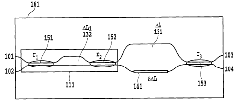
wavelength insensitiveness.
FIG. 7 is a plan view showing an interferometer optical
switch using the phase generating coupler 111. The power
coupling ratios of the directional couplers 151 and 152
constituting the phase generating coupler 111 were set at
rl = 0.3 and r2 = 0.7, and the path length difference of the
- 46 -
CA 02506387 2005-06-01
minute optical delay line 131 was set at AL1 = 0.30X c (;t; 0.47
m). In addition, the path length difference of the
Mach-Zehnder interferometer 131 was set at AL = 0.34Xc
0.53 m), and the power coupling ratio of the directional
coupler 153 was set at r3 = 0.5. Here, the path length
difference represents the relative optical path length of
the upper optical waveguide with respect to the lower optical
waveguide. The spacing between the two optical waveguides
interconnecting the optical multi/demultiplexing device 111
and the directional coupler 153 of the interferometer
optical switch was made 250 m. As the phase shifter 141,
a thin film heater was used and its width was set at 40 pm,
and length at 4 mm.
According to the foregoing design values, the
silica-based optical waveguide circuit was fabricated by
using flame hydrolysis deposition, photolithography
technique and reactive ion etching. It was fabricated such
that the relative refractive index of the optical waveguides
was 0.75% and the core cross section of the optical
waveguides was 6x6 m2.
A chip on which the interferometer optical switch was
formed was diced, and its switching characteristics were
evaluated. Here, the switching operation of a gate switch
will be described which uses the fabricated optical
waveguide circuit as a basic component.
- 47 -
CA 02506387 2005-06-01
When the phase shifter (thin film heater) 141 is in the
OFF state, the switch is in the bar state. Thus, the optical
signal input via the input waveguide 101 is output from the
output waveguide 103, but not from the output waveguide 104.
In this state, if the thin film heater 141 is activated, the
optical path length is varied by an amount of half wavelength
of the optical signal (0. 5Xc = k: where k is an integer other
than zero) by the thermooptic effect, and the path length
difference becomes AL + 6AL = 0.34kc - 0.5Xc = -0.16Xc. In
this case, the phase shifter (thin film heater) 141 is in
the ON state, and the switch is in the cross state. Thus,
the optical signal input via the input waveguide 101 is
output from the output waveguide 104. In other words, when
considering 101 as the input port, and 104 as the output port,
the optical signal is not output when the phase shifter is
in the OFF state, but is output when the phase shifter is
the ON state, which means that the switch functions as the
gate switch. When considering 102 as the input port, similar
switching operation was confirmed.
Next, FIG. 8 illustrates the wavelength characteristics
of the measured transmittance. The wavelength dependence
of the transmittance of the conventional Mach-Zehnder
interferometer optical switch as shown in FIG. 37 is also
illustrated for comparison.
When the phase shifter (thin film heater) 141 is in the
- 48 -
CA 02506387 2005-06-01
OFF state, the interferometer optical switch of the present
embodiment can achieve a high extinction ratio of greater
than or equal to 40 dB over a broad wavelength band of
1.45-1.6 m. When the phase shifter is brought into the ON
state, the interferometer optical switch of the present
embodiment achieves a good insertion loss over broad
wavelength band.
Thus, we confirmed that using the principle completely
different from that of the conventional technique, the
interferometer optical switch of the present embodiment
implements a compact switch that has a high extinction ratio
over a wide range and is operational with only one phase
shifter. In addition, since it carries out the switching
operation in the broad wavelength band, it has large
tolerance for the power coupling ratio error of the optical
multi/demultiplexing devices and the path length difference
error of the optical delay line. As a result, the present
embodiment implements an interferometer optical switch that
can maintain a high extinction ratio even if there is
fabrication error.
As described above, the interferometer optical switch
described in the present embodiment is designed such that
a high extinction ratio is obtained in a wavelength range
of 1.45-1.65 m. Besides, a high extinction ratio can be
obtained at any wavelength region, for example 1 um to 2 um,
- 49 -
CA 02506387 2005-06-01
by providing an appropriate phase with optimum design. In
addition, an optical multi/demultiplexing device composed
of N+l optical multi/demultiplexing devices and N optical
delay lines that connects adjacent optical
multi/demultiplexing devices is used as a phase generating
coupler, which is an optical coupler that is capable of
producing a wavelength-dependent phase difference. However,
it is obvious that other optical multi/demultiplexing
devices can also be used to realize a phase generating
coupler. Furthermore, its configuration is not limited to
that described in the present embodiment. For example, a
configuration is also possible which includes three optical
multi/demultiplexing devices and two optical delay lines
sandwiched between the adjacent optical
multi/demultiplexing devices. Alternatively, a
configuration is possible in which the phase generating
coupler is constructed by combining different optical
multi/demultiplexing devices. In addition, the optical
multi/demultiplexing devices are not limited to the
directional couplers the present embodiment uses, but other
types of couplers such as multimode interferometers can be
used. Besides, a plurality of types of optical
multi/demultiplexing devices can be used such as using a
directional coupler and a multimode interferometer as one
of and the other of the optical multi/demultiplexing devices
- 50 -
CA 02506387 2005-06-01
constituting the phase generating coupler.
Thus, the phase characteristics can be set considering
the wavelength dependence of the power coupling ratios of
the optical multi/demultiplexing devices used. In addition,
locally varying the refractive index of the optical
waveguides enables the adjustment of the optical path length
difference and of the coupling characteristics and phase
characteristics of the optical multi/demultiplexing devices.
Furthermore, although 101 and 102 are used as the input
waveguides in the present example, the same advantages are
obtained by using 103 and 104 as the input waveguides, and
101 and 102 as the output waveguides. Besides, although it
is designed in such a manner that m becomes -1, m can be +1
or some other integer.
As described above, the present invention is not limited
to the configuration described here. For example,
considering the entire circuit as a whole, it can configure
the interferometer optical switch capable of maintaining a
high extinction ratio over a broad band regardless of the
type of the waveguides, the geometry of the waveguides, the
material of the waveguides, wavelength band, or the type of
the optical multi/demultiplexing devices. The present
invention is implemented by setting the sum of the phase
difference of the outputs of the optical
multi/demultiplexing devices and the path length difference
- 51 -
CA 02506387 2005-06-01
of the optical delay line at a constant value in the
wavelength region or the frequency region being used.
(First Variation of First Embodiment)
A first variation of the first embodiment in accordance
with the present invention uses the same configuration as
the interferometer optical switch of the first embodiment
as shown in FIG. 7.
To meet the conditions that the power coupling ratio of
the phase generating coupler 111 is about 0.5 at the center
wavelength 7c = 1.55 m of the wavelength region, and the
phase difference between the output light satisfies the
foregoing expression (8), the power coupling ratios of the
two directional couplers 151 and 152, and the path length
difference of a minute optical delay line 132 were obtained
by polynomial approximation. As a result, the power coupling
ratios of the directional couplers 151 and 152 were set at
r1 = 0.1 and r2 = 0.6, respectively, the path length
difference of the minute optical delay line 132 was set at
AL1 = 0.27=Xc (;z~ 0.38 gm), and the power coupling ratio of
the directional coupler 153 was set at r3 = 0.5. In addition,
the path length difference of the Mach-Zehnder
interferometer was set at AL = 0.37 - Xc (;z:~ 0.53 m) , and the
spacing between the two optical waveguides interconnecting
the optical multi/demultiplexing device 111 and the
directional coupler 153 was made 250 m. Here, the path
52 -
CA 02506387 2005-06-01
length difference represents the relative optical path
length of the upper optical waveguide with respect to the
lower optical waveguide. As the phase shifter 141, a thin
film heater was used and its width was set at 40 m, and length
at 4 mm.
According to the foregoing design values, the
silica-based optical waveguide circuit was fabricated by
using flame hydrolysis deposition, photolithography
technique and reactive ion etching. It was fabricated such
that the relative refractive index of the optical waveguides
was 1. 5% and the core cross section of the optical waveguides
was 4.5x4.5 m2 Thus, the present example uses the
waveguides with the relative refractive index higher than
that of the conventional waveguides. This is because the
high relative refractive index of the waveguide can reduce
the minimum radius of curvature of the waveguides, and hence
can downsize the circuit, although the excess loss such as
a fiber coupling loss increases.
A chip on.which the interferometer optical switch was
formed was diced, a heatsink (not shown) was disposed under
the silicon substrate 161, single mode fibers (not shown)
were connected to the input/output waveguides 101-104, and
feeder leads (not shown) were connected to the thin film
heater 141, thereby forming a two-input, two-output optical
switch module. Forming the interferometer optical switch
- 53 -
CA 02506387 2005-06-01
of the present embodiment into a module can facilitate the
introduction of the switch to optical communication systems
such as optical cross connect systems and optical add/drop
multiplexing systems.
Next, the evaluation was made of the switching
characteristics of the fabricated interferometer optical
switch module. Here, the switching operation will be
described in the case where the switch module is used as the
gate switch using the fabricated optical waveguide circuit
as the basic component. When the phase shifter (thin film
heater) 141 is in the OFF state, the switch is in the bar
state. Thus, the optical signal input via the input
waveguide 101 is output from the output waveguide 103, but
not from the output waveguide 104. Although not shown in
FIG. 7, by supplying power to the thin film heater formed
on the upper side optical waveguide (first optical
waveguide) of the two delay lines of the optical delay line
131, the optical path length was varied by an amount
corresponding to half the wavelength of the optical signal
(0. 5X.c = k: k is an integer other than zero) by the thermooptic
effect, and the path length difference became AL + 8ML =
0.30Xc + 0.50?c = 0.8OXc. In this case, the switch was in
the cross state when the phase shifter (thin film heater)
141 was in the ON state, and hence the optical signal input
via the input waveguide 101 was output from the output
- 54 -
CA 02506387 2005-06-01
waveguide 104. Thus, we confirmed that the switch functions
as a gate switch. Although the foregoing k is assumed to
have a value +1 in the present example, it is obvious that
k can take other values.
FIG. 9 illustrates the wavelength characteristics of the
measured transmittance. The wavelength dependence of the
transmittance of the conventional Mach-Zehnder
interferometer optical switch as shown in FIG. 37 is also
illustrated for comparison. When the phase shifter was in
the OFF state, the interferometer optical switch of the
present embodiment was able to achieve a high extinction
ratio in a broader wavelength band than the conventional
optical switch. When the phase shifter was brought into the
ON state, the interferometer optical switch of the present
embodiment achieved a good insertion loss in the broad
wavelength band.
(Second Variation of First Embodiment)
A second variation of the first embodiment in accordance
with the present invention uses the same configuration as
the interferometer optical switch of the first embodiment
shown in FIG. 7.
To meet the conditions that the power coupling ratio of
the phase generating coupler Ill is about 0.45 at the center
wavelength Xc = 1.55 pm of the wavelength region, and the
phase difference between the output light satisfies the
- 55 -
CA 02506387 2005-06-01
foregoing expression (8), the power coupling ratios of the
two directional couplers 151 and 152, and the path length
difference of the minute optical delay line 132 were obtained
by least square approximation. As a result, the power
coupling ratios of the directional couplers 151 and 152 were
set at r1 = 0.4 and r2 = 0.8, respectively, the path length
difference of the minute optical delay line 132 was set at
AL1 = 0.30=Xc (~ 0.47 m), and the power coupling ratio of
the directional coupler 153 was set at r3 = 0.5. In addition,
1o the path length difference of the Mach-Zehnder
interferometer was set at AL = 0.32 - Xc (;zl 0.50 m) , and the
spacing between the two optical waveguides interconnecting
the optical multi/demultiplexing device 111 and the
directional coupler 153 was made 250 m. Here, the path
length difference represents the relative optical path
length of the upper optical waveguide with respect to the
lower optical waveguide. As the phase shifter, a thin film
heater was used and its width was set at 40 pm, and length
at 4 mm. As for the path length difference of the
Mach-Zehnder interferometer, it was initially set at AL =
0 pm, and after the circuit was fabricated, permanent local
heat processing with a thin film heater was carried out to
vary the refractive index of the waveguides, thereby
adjusting the optical path length difference to AL = 0.32Xc
(~ 0.50 gm) .
56 -
CA 02506387 2005-06-01
Thus, in this invention, the optical path length refers
to the effective optical path length of the waveguide, which
takes into consideration both the wavelength-dependent
refractive index and the path length of the waveguide.
Accordingly, the optical path length can be altered by
varying the refractive index of the waveguides even after
forming the waveguides. Consequently, after the
interferometer optical switch with the path length
difference of zero has been formed, the optical path length
difference can be adjusted to the design value by varying
the refractive index of the waveguides in the fabrication
process. In addition, the fabrication error can be removed
by using the permanent local heat processing using the thin
film heater. In other words, even if the optical path length
difference deviates from the design value because of the
fabrication error, the path length difference can be
corrected to the design value by adjusting the refractive
index after the fabrication. Incidentally, the reason why
the present embodiment uses the thin film heater is that the
thin film heater has already been formed on the optical
waveguide as the phase shifter. Besides, the thin film
heater formed on the optical waveguide enables the
refractive index to be adjusted simply and accurately. It
is needless to say that the adjusting method of the
refractive index is not limited to the thin film heater, but
57 -
CA 02506387 2005-06-01
other means such as light irradiation with a laser can also
be used. In addition, although the present embodiment uses
the thin film formed for the switching operation to perform
the local heat treatment, another thin film heater can be
installed to be used specifically for the local heat
treatment to adjust the refractive index. Furthermore, the
characteristics of the optical multi/demultiplexing device
111 can be corrected by adjusting the refractive index of
the optical waveguides of the directional couplers 151 and
152 or of the minute optical delay line 132 constituting the
optical multi/demultiplexing device 111.
According to the foregoing design values, the
silica-based optical waveguide circuit was fabricated by
using flame hydrolysis deposition, photolithography
technique and reactive ion etching. It was fabricated such
that the relative refractive index of the optical waveguides
was 0.75%, and the core cross section of the optical
waveguides was 6x6 m2
A chip on.which the interferometer optical switch was
formed was diced, a heatsink (not shown) was disposed under
the silicon substrate 161, dispersion shifted fibers (not
shown) were connected to the input/output waveguides 101-104,
and feeder leads (not shown) were connected to the thin film
heater 141, thereby forming a two-input, two-output optical
switch module.
- 58 -
CA 02506387 2005-06-01
Next, the evaluation was made of the switching
characteristics of the interferometer optical switch module
fabricated as described above. Here, the switching
operation will be described in the case where the switch is
used as the gate switch employing the fabricated optical
waveguide circuit as the basic component. When the phase
shifter (thin film heater) 141 is in the OFF state, the switch
is in the bar state. Thus, the optical signal input via the
input waveguide 101 is output from the output waveguide 103,
1o but not from the output waveguide 104. Here, by supplying
power to the thin film heater 141, the optical path length
was varied by an amount corresponding to half the wavelength
of the optical signal (0.5?c=k: k is an integer other than
zero) by the thermooptic effect, and the path length
difference became AL + SAL = 0.32Xc - 0.50Xc = -0.182c. In
this case, the switch was in the cross state when the phase
shifter (thin film heater) 141 was in the ON state, and hence
the optical signal input via the input waveguide 101 was
output from the output waveguide 104. Thus, we confirmed
that the switch functions as a gate switch.
FIG. 10 illustrates the wavelength characteristics of
the measured transmittance. The wavelength dependence of
the transmittance of the conventional Mach-Zehnder
interferometer optical switch as shown in FIG. 37 is also
illustrated for comparison. When the phase shifter was in
- 59 -
CA 02506387 2005-06-01
the OFF state, the interferometer optical switch of the
present embodiment achieved an extinction ratio greater
than or equal to 30 dB over a broad wavelength band of
1.45-1.63 m. When the phase shifter was brought into the
ON state, the interferometer optical switch of the present
embodiment achieved a good insertion loss over the broad
wavelength band. Although the present example is designed
such that the power coupling ratio (0.45) of the first
optical multi/demultiplexing device (phase generating
coupler 111) and the power coupling ratio (0.5) of the second
optical multi/demultiplexing device (directional coupler
153) differ from each other, it can achieve a high extinction
ratio over a broader wavelength band than the conventional
optical switch. Thus, the first and second optical
multi/demultiplexing devices can have different power
coupling ratios, and the power coupling ratios can have
different wavelength dependence.
(SECOND EMBODIMENT)
FIG. 11 shows a configuration of the interferometer
optical switch of a second embodiment in accordance with the
present invention. The circuit of the interferometer
optical switch includes a pair of optical
multi/demultiplexing devices (phase generating couplers)
111 and 112, the phase differences of the outputs of which
have wavelength dependence; an optical delay line 131
- 60 -
CA 02506387 2005-06-01
between the optical multi/demultiplexing devices 111 and
112; phase shifters (thin film heaters) 141 formed in the
optical delay line 131; input waveguides 101 and 102; and
output waveguides 103 and 104.
In the present embodiment, a configuration will be
described which includes a plurality of phase generating
couplers. Assume that a light is input to the phase
generating coupler 111 in the first stage, and the phase
difference between light output from the two optical
to waveguides connected to the phase generating coupler 111 is
~1(X); and that light are launched into the two optical
waveguides connected to the phase generating coupler 112 at
the second stage, and the phase difference between the light
output from the phase generating coupler 112 is ~2 (?) . Then,
the wavelength-dependent phase differences of the outputs
of the phase generating couplers 111 and 112 is set to satisfy
the following expression.
4 (X) +42 (X)=0L/X + m/2 (9).
Where m is an integer.
Here, the optical multi/demultiplexing device (phase
generating coupler) as shown in FIG. 4 is used as the phase
generating couplers 111 and 112. The optical
multi/demultiplexing device (phase generating coupler) as
- 61 -
CA 02506387 2005-06-01
shown in FIG. 4 includes two directional couplers 151 and
152; a minute optical delay line 132 consisting of the two
optical waveguides interconnecting the two directional
couplers 151 and 152; input waveguides 101 and 102; and
output waveguides 103 and 104. To meet the conditions that
the power coupling ratios of the optical
multi/demultiplexing devices become about 0.5 at the center
wavelength 2c = 1.55 m of the wavelength region, and the
phase difference between the output light satisfies the
foregoing expression (9), the power coupling ratios of the
two directional couplers 151 and 152 constituting the phase
generating couplers, and the path length difference of the
minute optical delay line 132 were obtained by least square
approximation.
FIG. 12 illustrates the sum of the phase differences of
the phase generating couplers 111 and 112 thus designed. At
the same time, the required phase T(X) to be corrected by
the phase generating couplers, that is, the desired function
given by the right side of the foregoing expressions (9) is
drawn. In FIG. 12, AL is set at 0.l6Xc (,& 0.25 m), and m
is set at -1 as a numerical example. It is seen from FIG.
12 that the two phase generating couplers each function as
a 3 dB optical multi/demultiplexing device with the power
coupling ratio of about 0.5, and that the sum of the phase
differences 4i (?) + j2 (X) is nearly equal to the required
- 62 -
CA 02506387 2005-06-01
phase 'P(2) required for achieving the wavelength
insensitiveness.
FIG. 13 is a plan view showing an actually fabricated
interferometer optical switch. The power coupling ratios
of the directional couplers 151 and 152 constituting the
phase generating coupler 111 were set at r1 = 0.4 and r2 =
0.1. As for the minute optical delay line 132 having two
optical delay lines, a first optical waveguide and a second
optical waveguide, their optical path lengths are set at 11,
= 502.32 m and 121 = 501.99 m so that the optical path length
difference between them is AL1 = 111 - 121 = 0.21Xc (= 0.33
m). Likewise, the power coupling ratios of the directional
couplers 153 and 154 constituting the other phase generating
coupler 112 are set at r3 = 0.2 and r4 = 0.3. As for the
minute optical delay line 133 having two optical delay lines,
a first optical waveguide and a second optical waveguide,
their optical path lengths are set at 112 = 463.94 m and 122
= 463.68 m so that the optical path length difference
between them i.s AL2 = 112 - 122 = 0. 17k c (= 0.26 m) . In addition,
the present embodiment employs two phase generating couplers,
and their optical delay lines are disposed in such a manner
that the optical delay lines having a greater sum of the
optical path lengths are placed disproportionately on one
side (upper side of FIG. 13) . More specifically, since E11,1
= 111, Y-12,1 = 121, Y-11,2 = 112, and Y-12,2 = 122, they satisfy Y-11,1
- 63 -
CA 02506387 2005-06-01
> E12,1 and F111,2 > Y-12,2- In addition, the path length
difference of the Mach-Zehnder interferometer is set at AL
= 0. 16Xc (~z-, 0.25 m) , and the spacing between the two optical
waveguides interconnecting the optical
multi/demultiplexing devices 111 and 112 was made 200 pm.
As the phase shifter 141, a thin film heater was used and
its width was set at 40 m, and length at 4 mm.
According to the foregoing design values, the
silica-based optical waveguide circuit was fabricated by
1o using flame hydrolysis deposition, photolithography
technique and reactive ion etching. It was fabricated such
that the relative refractive index of the optical waveguides
was 1.5%, and the core cross section of the optical
waveguides was 4.5x4.5 m2
A chip on which the interferometer optical switch was
formed was diced, a heatsink (not shown) was disposed under
the silicon substrate 161, single mode fibers (not shown)
were connected to the input/output waveguides 101-104, and
feeder leads (not shown) were connected to the thin film
heater 141, thereby forming a two-input, two-output optical
switch module. Then, the switching characteristics of the
interferometer optical switch module were evaluated.
Here, the switching operation will be described in the
case where the switch module is used as the gate switch using
the fabricated optical waveguide circuit as the basic
- 64 -
CA 02506387 2005-06-01
component. When the phase shifter (thin film heater) 141
is in the OFF state, the switch is in the bar state. Thus,
the optical signal input via the input waveguide 101 is
output from the output waveguide 103, but not from the output
waveguide 104. Here, by supplying power to the thin film
heater 141, the optical path length was varied by an amount
corresponding to half the wavelength of the optical signal
(0.5Xc= k: k is an integer other than zero) by the thermooptic
effect, and the path length difference became AL + SQL =
0.16Xc - 0.5Xc = -0.34Xc. In this case, the switch was in
the cross state when the phase shifter (thin film heater)
141 was in the ON state, and hence the optical signal input
via the input waveguide 101 was output from the output
waveguide 104. In other words, when considering 101 as the
input port, and 104 as the output port, the optical signal
is not output when the phase shifter is in the OFF state,
but is output when the phase shifter is the ON state, which
means that the switch functions as the gate switch. When
considering the 102 as the input port, similar switching
operation was confirmed.
Next, FIG. 14 illustrates the wavelength characteristics
of the measured transmittance of the interferometer optical
switch of the present embodiment. The wavelength dependence
of the transmittance of the conventional Mach-Zehnder
interferometer optical switch as shown in FIG. 37 is also
- 65 -
CA 02506387 2005-06-01
illustrated for comparison. When the phase shifter 141 is
in the OFF state, the interferometer optical switch of the
present embodiment can achieve a high extinction ratio equal
to or greater than 40 dB over a broad wavelength band of
1.45-1.6 m. When the phase shifter is brought into the ON
state, the interferometer optical switch of the present
embodiment achieves a good insertion loss over a broad
wavelength band.
Thus, the interferometer optical switch described in the
l0 present embodiment uses a novel operation principle to
implement high extinction ratio over a wide wavelength
region. It was confirmed that the switch is operational with
only one phase shifter. In addition, the switch has a larger
tolerance as regards power coupling ratio variations of the
optical multi/demultiplexing device and path length
variations of the optical delay line, since it is operational
over a wide wavelength range. Accordingly, the present
embodiment implements an interferometer optical switch that
can maintain a high extinction ratio even if there is
fabrication error.
Since the present embodiment employs two different phase
generating couplers, it can increase the phase compensation
amount and the degree of approximation of the power coupling
ratios of the optical multi/demultiplexing devices, thereby
being able to achieve characteristics better than that of
66 -
CA 02506387 2005-06-01
the first embodiment. In addition, an ideal Mach-Zehnder
interferometer optical switch is implemented when the power
coupling ratios of the first and second optical
multi/demultiplexing devices are 0.5 regardless of the
wavelength. Since the present embodiment is configured such
that it can set the phase differences and the power coupling
ratios of the first and second optical multi/demultiplexing
devices without restraint, it can implement an ideal
interferometer optical switch.
As described above, the interferometer optical switch
described in the present embodiment is designed such that
it can achieve a high extinction ratio in a wavelength band
of 1.45-1.65 m. However, the present invention is not
limited to this wavelength region. The switch can achive a
high extinction ratio at any wavelength region, for example
1 m - 2 m, by providing an appropriate phase with phase
generating coupler. Furthermore, an optical
multi/demultiplexing device composed of N + 1 optical
multi/demultiplexing devices and N optical delay lines that
connects adjacent optical multi/demultiplexing devices is
used as a phase generating coupler, which is an optical
coupler that is capable of producing a wavelength-dependent
phase difference. However, it is obvious that optical
multi/demultiplexing device with other configuration can be
used as the phase generating coupler. Besides, the
- 67 -
CA 02506387 2005-06-01
configuration is not limited to that described in the present
embodiment. For example, the optical multi/demultiplexing
device that is used as the phase generating coupler can be
configured by four optical multi/demultiplexing devices and
three optical delay lines sandwiched between the adjacent
optical multi/demultiplexing devices, or can be configured
by combining different optical multi/demultiplexing devices.
Furthermore, as for the optical multi/demultiplexing
devices used in the present embodiment to construct the
optical multi/demultiplexing device that generates a
wavelength-dependent phase difference, they are not limited
to the directional couplers, but other types can also be used.
In addition, the phase characteristics can be set
considering the wavelength dependence of the power coupling
ratios of the optical multi/demultiplexing devices used.
Besides, it is possible, in the present embodiment, to adjust
the optical path length difference, and the coupling
characteristics and phase characteristics of the optical
multi/demulti.plexing device by locally varying the
refractive index of the optical waveguides. ggg, although
the present example employs the waveguides 101 and 102 as
the input waveguides, it can achieve the same advantages by
using the waveguides 103 and 104 as the input waveguides,
and 101 and 102 as the output waveguides. Finally, although
the present example is designed such that m in the foregoing
- 68 -
CA 02506387 2005-06-01
expression (9) becomes -1, m may be + 1 or any other integer.
As described above, the present invention is not limited
to the configuration described here, but can configure the
interferometer optical switch that can maintain a high
extinction ratio over a broad band regardless of the types
of the waveguides, the geometry of the waveguides, the
material of the waveguides, wavelength band or the types of
the optical multi/demultiplexing device by making the sum
of the phase differences of the outputs of the optical
1o multi/demultiplexing devices and the phase difference due
to the path length difference of the optical delay line
constituting the circuit a constant value in the entire
wavelength or frequency band considering the circuit in its
entirety.
(THIRD EMBODIMENT)
FIG. 15 shows a configuration of the interferometer
optical switch of a third embodiment in accordance with the
present invention. The circuit of the interferometer
optical switch of the present embodiment includes an optical
multi/demultiplexing device (phase generating coupler) 111,
the phase difference of the output of which has wavelength
dependence; a directional coupler 153; an optical delay line
131 between the optical multi/demultiplexing device 111 and
the directional coupler 153; phase shifters 141 formed in
the optical delay line 131; input waveguides 101 and 102;
- 69 -
CA 02506387 2005-06-01
and output waveguides 103 and 104. As the phase generating
coupler 111, the present embodiment uses an optical
multi/demultiplexing device that includes two directional
couplers 151 and 152, and a minute optical delay line 132
composed of two optical waveguides interconnecting the two
directional couplers 151 and 152. In addition, three
adiabatic grooves 168 are formed at the sides of the pair
of phase shifters 141 on a substrate.
FIG. 16 shows the cross sectional structure taken along
the line XVI-XVI of the interferometer optical switch as
shown in FIG. 15. On a silicon substrate 161, cladding glass
layers 164 and 167 composed of silica-based glass are stacked.
As a mid layer of the cladding glass layers 164 and 167, a
core glass section 165 made from the silica-based glass is
is disposed, which constitutes the optical waveguides. In
addition, on a surface of the overcladding glass layer 167,
the phase shifters (thin film heaters) 141 are formed, and
at both sides of the phase shifters 141, the adiabatic
grooves 168 are formed. The adiabatic grooves 168 are
located at such position that equalizes the stress near core
waveguides.
To meet the conditions that the power coupling ratio of
the phase generating coupler 111 is about 0.5 at the center
wavelength Xc = 1.55 m of the wavelength region, and the
phase difference between the output light satisfies the
- 70 -
CA 02506387 2005-06-01
foregoing expression (8), the power coupling ratios of the
two directional couplers 151 and 152, and the path length
difference of the minute optical delay line 132 were obtained
by polynomial approximation. As a result, the power coupling
ratios of the directional couplers 151 and 152 were set at
r, = 0.1 and r2 = 0.6, respectively, the path length
difference of the minute optical delay line 132 was set at
AL1 = 0.27=kc (,:z 0.38 m), and the power coupling ratio of
the directional coupler 153 was set at r3 = 0.5. In addition,
the path length difference of the Mach-Zehnder
interferometer was set at AL = 0.37 =7 c (;:z~ 0.53 m) , and the
spacing between the two optical waveguides interconnecting
the optical multi/demultiplexing device 111 and the
directional coupler 153 was made 100 m. Here, the path
length difference represents a relative optical path length
of the upper optical waveguide with respect to the lower
optical waveguide. As the phase shifters 141, a thin film
heater was used and its width was set at 40 m, and length
at 4 mm.
According to the foregoing design values, the
silica-based optical waveguide circuit was fabricated by
using flame hydrolysis deposition, photolithography
technique and reactive ion etching. It was fabricated such
that the relative refractive index of the optical waveguides
was 0.75%, the core cross section of the optical waveguides
- 71 -
CA 02506387 2005-06-01
was 6x6 m2, and the width and the depth of the adiabatic
grooves 168 were 70 pm and 35 m, respectively.
A chip on which the interferometer optical switch was
formed was diced, a heatsink (not shown) was disposed under
the silicon substrate 161, single mode fibers (not shown)
were connected to the input/output waveguides 101-104, and
feeder leads (not shown) were connected to the thin film
heaters 141, thereby forming a two-input, two-output optical
switch module. Then, the switching characteristics of the
interferometer optical switch module were evaluated.
Here, the switching operation will be described in the
case where the switch module is used as the gate switch using
the fabricated optical waveguide circuit as the basic
component. When the phase shifters (thin film heaters) 141
are in the OFF state, the switch is in the bar state. Thus,
the optical signal input via the input waveguide 101 is
output from the output waveguide 103, but not from the output
waveguide 104. By supplying power to the thin film heaters
141, the optical path length was varied by an amount
corresponding to half the wavelength of the optical signal
(0 .5Xc = k: k is an integer other than zero) by the thermooptic
effect, and the path length difference became AL + SAL =
0 . 37? c + 0 . 50? c = -0 . 13? c. In this case, the switch was in
the cross state when the phase shifters (thin film heaters)
141 were in the ON state, and hence the optical signal input
72 -
CA 02506387 2005-06-01
via the input waveguide 101 was output from the output
waveguide 104. In other words, when using the waveguide 101
as the input port and 104 as the output port, the optical
signal was not output when the phase shifters 141 were in
the OFF state, but was output when the phase shifters 141
were in the ON state, which means that the switch functions
as a gate switch. We confirmed the same switching operation
when using the waveguide 102 as the input port. In addition,
although the present example employs the waveguides 101 and
102 as the input waveguides, it can achieve the same
advantages by using the waveguides 103 and 104 as the input
waveguides, and 101 and 102 as the output waveguides.
Besides, since the optical switch of the present embodiment
has the adiabatic groove structure, it can suppress the power
consumption of the phase shifters required for the switching
to 1/10 that of the conventional switch.
Next, FIG. 17 illustrates the wavelength dependence of
the transmittance measured for the circuit of the present
embodiment. The optical switch of the present embodiment
can also achieve a high extinction ratio equal to or greater
than 30 dB over a broad wavelength band of 1.3-1.6 m when
the phase shifters are in the OFF state.
Thus, the interferometer optical switch described in
the present embodiment uses a novel operation principle to
implement high extinction ratio over a wide wavelength
- 73 -
CA 02506387 2005-06-01
region. It was confirmed that the switch is operational with
only one phase shifter. In addition, the switch has a larger
tolerance as regards power coupling ratio variations of the
optical multi/demultiplexing device and path length
variations of the optical delay line, since it is operational
over a wide wavelength range. Accordingly, the present
embodiment implements an interferometer optical switch that
can maintain a high extinction ratio even if there is
fabrication error. In addition, since the interferometer
optical switch of the present embodiment has the adiabatic
groove structure on the substrate, it can greatly reduce the
switching power. It is obvious that the geometry and
position of the grooves are not limited, and the grooves can
include materials other than air, and that a structure other
than the optical circuit can be formed on the planar
substrate as illustrated in the present embodiment.
(FOURTH EMBODIMENT)
FIG. 18 shows a configuration of the interferometer
optical switch of a fourth embodiment in accordance with the
present invention. The circuit of the interferometer
optical switch of the present embodiment is an optical switch
with a multiple-stage interferometer configuration using a
plurality of interferometer optical switches. Since the
multiple-stage interferometer configuration can block light
with plurality of basic components when the switch is in the
- 74 -
CA 02506387 2005-06-01
OFF state, it can achieve an extinction ratio higher than
that of the single basic component.
The present circuit is configured by connecting two
interferometer optical switches of the first embodiment as
shown in FIG. 7. A first stage (input side) interferometer
optical switch 170 has its first output (corresponding to
104 of FIG. 7) connected to a first input (corresponding to
102 of FIG. 7) of a second stage (output side) interferometer
optical switch 171, and has its second output (corresponding
to 103 of FIG. 7) used as the output waveguide 103. The second
stage interferometer optical switch 171 has its second input
(corresponding to 101 of FIG. 7) used as the input waveguide
101. The input waveguide 101 and the output waveguide 103
intersect with each other on the way, thereby forming a cross
waveguide 155. It is obvious that such a circuit layout is
also possible in which the input waveguide and output
waveguide do not intersect with each other. In addition,
the interferometer optical switch 170 of the first stage has
its second input (corresponding to 101 of FIG. 7) used as
the input waveguide 102, and the interferometer optical
switch 171 of the second stage has its second output
(corresponding to 103 of FIG. 7) used as the output waveguide
104.
To meet the conditions that the power coupling ratios of
the phase generating couplers are about 0.5 at the center
- 75 -
CA 02506387 2005-06-01
wavelength ?,c = 1.55 m of the wavelength region, and the
phase difference between the output light satisfies the
foregoing expression (8), the power coupling ratios of the
two directional couplers 151 and 152, and the path length
difference of the minute optical delay line 132 were obtained
by the conjugate gradient method. As a result, the power
coupling ratios of the directional couplers 151 and 152 were
set at r1 = 0.3 and r2 = 0.7, respectively, the path length
difference of the minute optical delay line 132 was set at
1o AL1 = 0.30 = 2 c 0.47 W), and the power coupling ratio of
the directional coupler 153 was set at r3 = 0.5. In addition,
the path length difference of the Mach-Zehnder
interferometer was set at AL = 0.34 = Xc (;::~ 0.53 m) , and the
spacing between the two optical waveguides interconnecting
the optical multi/demultiplexing device 111 and the
directional coupler 153 was made 100 m. Here, the path
length difference represents the relative optical path
length of the upper optical waveguide with respect to the
lower optical waveguide. As the phase shifters 141, a thin
film heater was used and its width was set at 40 m, and length
at 4 mm. The path length difference of the Mach-Zehnder
interferometer was initially set at AL = 0 m, and after the
circuit was fabricated, permanent local heat processing
using the thin film heaters 141 was carried out to adjust
the optical path length difference to AL = 0.34?c (,z~ 0.53
- 76 -
CA 02506387 2005-06-01
m).
Although the present embodiment forms two thin film
heaters 141 on each of the pair of the optical waveguides
constituting the optical delay line 131, and uses one for
the local heat processing and the other for the switching
operation, it is also possible to use both for the local heat
processing, or for the switching operation. It is obvious
that three or more thin film heaters can be formed. In
addition, the geometry of the thin film heaters 141 is not
limited, and the plurality of thin film heaters can have
different geometry. Furthermore, the thin film heaters 141
of the pair of the optical waveguides constituting the
optical delay line 131 can be used simultaneously to carry
out the local heat processing or the switching operation.
According to the foregoing design values, the
silica-based optical waveguide circuit was fabricated by
using flame hydrolysis deposition, photolithography
technique and reactive ion etching. It was fabricated such
that the relative refractive index of the optical waveguides
was 0.75%, the core cross section of the optical waveguides
was 4.5x4.5 m2 , and the width and the depth of the adiabatic
grooves were 70 m and 50 m, respectively.
A chip on which the interferometer optical switch was
formed was diced, a heatsink (not shown) was disposed under
the silicon substrate 161, dispersion shifted fibers (not
- 77 -
CA 02506387 2005-06-01
shown) were connected to the input/output waveguides 101-104,
and feeder leads (not shown) were connected to the thin film
heaters 141, thereby forming a two-input, two-output optical
switch module. Then, the switching characteristics of the
interferometer optical switch module were evaluated.
When the phase shifters (thin film heaters) 141 are in
the OFF state, the switch is in the bar state. Thus, the
optical signal input via the input waveguide 102 is output
from the output waveguide 103, but not from the output
waveguide 104. In this case, since the two basic components
170 and 171 block light from launching out of the output
waveguide 104, the present embodiment can achieve a higher
extinction ratio. By supplying power to the thin film
heaters 141 of the interferometer optical switches 170 and
171, the optical path length was varied by an amount
corresponding to half the wavelength of the optical signal
(0.5Ac=k: k is an integer other than zero) by the thermooptic
effect, and the path length difference became AL + 6AL =
0.347c - 0 . 50? c = -0 .16? c . In this case, the switch was in
the cross state when the phase shifters (thin film heaters)
141 were in the ON state, and hence the optical signal input
via the input waveguide 102 was output from the output
waveguide 104. In other words, when using the waveguide 101
as the input port and 104 as the output port, the optical
signal was not output when the phase shifters 141 were in
- 78 -
CA 02506387 2005-06-01
the OFF state, but was output when the phase shifters 141
were in the ON state, which means that the switch functions
as a gate switch. In addition, although the present example
employs the waveguides 101 and 102 as the input waveguides,
it can achieve the same advantages by using the waveguides
103 and 104 as the input waveguides, and 101 and 102 as the
output waveguides. Besides, since the optical switch of the
present embodiment has the adiabatic groove structure, it
can suppress the power consumption of the phase shifters
required for the switching to 1/10 of the conventional
switch.
Next, FIG. 19 illustrates the wavelength characteristics
of the measured transmittance of the interferometer optical
switch of the present embodiment. The wavelength dependence
of the transmittance of the conventional Mach-Zehnder
interferometer optical switch as shown in FIG. 37 is also
illustrated for comparison. When the phase shifters 141 are
in the OFF state, the interferometer optical switch of the
present embodiment can achieve a high extinction ratio equal
to or greater than 60 dB over a broad wavelength band of
1.45-1.63 m because of the multiple-stage interferometer
configuration. When the phase shifters are brought into the
ON state, the interferometer optical switch of the present
embodiment achieves a good insertion loss over a broad
wavelength band.
- 79 -
CA 02506387 2005-06-01
As described above, the plurality of interferometer
optical switches in accordance with the present invention,
which are configured in a multiple stage, enable them to
function as a single interferometer optical switch.
Although the present embodiment constructs the two-stage
interferometer configuration by combining the two identical
interferometer optical switches, it is obvious that the two
interferometer optical switches can use different design
values. In addition, it is also possible to assume a
configuration other than the two-stage interferometer
configuration described in the present embodiment. Besides,
it is also possible to use any desired optical waveguides
as the input waveguides and output waveguides by
interconnecting any desired optical waveguides.
Furthermore, it is also possible to combine three or more
interferometer optical switches with the same structure, or
to combine a plurality of interferometer optical switches
with different structures.
As described above, using the interferometer optical
switch of the present embodiment enables the switching
operation over the broad wavelength band. In addition, since
the interferometer optical switch of the present embodiment
can carry out switching operation over the broad wavelength
band, it has a great tolerance for the power coupling ratio
error of the optical multi/demultiplexing devices or for the
- 80 -
CA 02506387 2005-06-01
path length difference error of the optical delay lines.
Accordingly, the present embodiment implements an
interferometer optical switch that can maintain a high
extinction ratio even if there is fabrication error.
(First Variation of Fourth Embodiment)
FIG. 20 shows a configuration of the interferometer
optical switch of a first variation of the fourth embodiment
in accordance with the present invention. The circuit of
the variation is an optical switch with a multiple-stage
interferometer configuration using two interferometer
optical switches described in the second embodiment as shown
in FIG. 13. With such a multiple-stage interferometer
configuration, the switch can achieve an extinction ratio
higher than that of the single basic component because it
can prevent the leakage light with the plurality of basic
components 170 and 171 in the OFF state.
The multiple-stage interferometer optical switch of the
present example has two basic components of FIG. 13 arranged
in line symmetry with respect to the center of the circuit.
Then, the interferometer optical switch 170 in the first
stage has its first output (corresponding to 104 of FIG. 13)
connected to a first input (corresponding to 102 of FIG. 13)
of the interferometer optical switch 171 in the second stage,
and has its second output (corresponding to 103 of FIG. 13)
used as the output waveguide 103. The interferometer optical
- 81 -
CA 02506387 2005-06-01
switch 171 in the second stage has its second input
(corresponding to 101 of FIG. 13) used as the input waveguide
101. The input waveguide 101 and the output waveguide 103
intersect with each other on the way, thereby forming a cross
waveguide 155. In addition, the interferometer optical
switch 170 of the first stage has its second input
(corresponding to 101 of FIG. 13) used as the input waveguide
102, and the interferometer optical switch 171 of the second
stage has its second output (corresponding to 103 of FIG.
13) used as the output waveguide 104. It is obvious that
the two basic components 170 and 171 can be disposed in the
same direction as in the foregoing fourth embodiment or can
be disposed in the opposite direction. As for the circuit
layout, it is not limited: the two basic components 170 and
171 can be disposed in the horizontal direction as shown in
FIG. 20, or in the vertical direction.
The interferometer optical switches 170 and 171
constituting the multiple-stage interferometer of this
example use the same design values. The power coupling
ratios of the two directional couplers 151 and 152 and 153
and 154, and the path length differences of the minute
optical delay lines 132 and 133 constituting the phase
generating couplers were obtained by using the multiple
regression analysis in such a manner that the power coupling
ratios of the phase generating couplers 111 and 112 (see FIG.
82 -
CA 02506387 2005-06-01
13) became about 0.5 at the center wavelength Xc = 1.55 pm
of the wavelength region and that the phase difference
between the output light satisfied the foregoing expression
(9). As a result, the power coupling ratios of the
directional couplers 151 and 152 constituting the first
phase generating coupler 111 were set at r1 = 0.3 and r2 =
0.1, respectively, and the path length difference of the
minute optical delay line 132 was set at AL1 = 0.19Xc (,& 0.29
m). Here, the path length difference represents the
relative optical path length of the upper optical waveguide
with respect to the lower optical waveguide. Likewise, the
power coupling ratios of the directional couplers 153 and
154 constituting the second phase generating coupler 112
were set at r1 = 0.1 and r2 = 0.3, respectively, and the path
length difference of the minute optical delay line 133 was
set at AL2 = 0.19Xc (& 0.29 m) . In addition, the path length
difference of the Mach-Zehnder interferometer was set at AL
= 0. 16Xc (;::~ 0.25 m) , and the spacing between the two optical
waveguides interconnecting the optical
multi/demultiplexing devices 111 and 112 was made 100 pm.
As the phase shifters 141, a thin film heater was used and
its width was set at 40 pm, and length at 4 mm.
According to the foregoing design values, the
silica-based optical waveguide circuit was fabricated by
using flame hydrolysis deposition, photolithography
- 83 -
CA 02506387 2005-06-01
technique and reactive ion etching. It was fabricated such
that the relative refractive index of the optical waveguides
was 1.5%, the core cross section of the optical waveguides
was 4 .5x4 .5 m2 , and the width and the depth of the adiabatic
grooves 168 were 70 m and 50 m, respectively.
A chip on which the interferometer optical switch was
formed was diced, a heatsink (not shown) was disposed under
the silicon substrate 161, single mode fibers (not shown)
were connected to the input/output waveguides 101-104, and
feeder leads (not shown) were connected to the thin film
heaters 141, thereby forming a two-input, two-output optical
switch module. Then, the switching characteristics of the
interferometer optical switch module were evaluated.
When the phase shifters (thin film heaters) 141 are in
the OFF state, the switch is in the bar state. Thus, the
optical signal input via the input waveguide 102 is output
from the output waveguide 103, but not from the output
waveguide 104. In this case, since the two basic components
170 and 171 prevent leakage light from coming out of the
output waveguide 104, the present embodiment can achieve a
higher extinction ratio. By supplying power to the thin film
heaters 141 of the interferometer optical switches 170 and
171, and varying the optical path length by an amount
corresponding to half the wavelength of the optical signal
(0. 5A,c = k: k is an integer other than zero) by the thermooptic
- 84 -
CA 02506387 2005-06-01
effect, the path length difference became AL - ML = 0.16Xc
- 0.50Xc = -0.34Xc. In this case, the phase shifters (thin
film heaters) 141 were in the ON state, and the switch was
in the cross state, and hence the optical signal input via
the input waveguide 102 was output from the output waveguide
104. In addition, although the present example employs the
waveguides 101 and 102 as the input waveguides, it can
achieve the same advantages by using the waveguides 103 and
104 as the input waveguides, and 101 and 102 as the output
waveguides. Besides, since the optical switch of the present
example has the adiabatic groove structure, it can suppress
the power consumption of the phase shifters required for the
switching to 1/10 that of the conventional switch.
Next, FIG. 21 illustrates the wavelength characteristics
of the measured transmittance of the interferometer optical
switch of the present example. The wavelength dependence
of the transmittance of the conventional Mach-Zehnder
interferometer optical switch as shown in FIG. 37 is also
illustrated for comparison.
When the phase shifters 141 are in the OFF state, the
interferometer optical switch of the present example can
achieve a high extinction ratio equal to or greater than 60
dB over a broad wavelength band of 1.45-1.65 m, and equal
to or greater than 80 dB over a broad wavelength band of
1.45-1.63 m because of the multiple-stage interferometer
- 85 -
CA 02506387 2005-06-01
configuration. When the phase shifters are brought into the
ON state, the interferometer optical switch of the present
example achieves a good insertion loss over a broad
wavelength band.
As described above, using the plurality of
interferometer optical switches in accordance with the
present invention enables them to function as a single
interferometer optical switch. Although the present example
constructs the two-stage interferometer configuration by
combining the two identical interferometer optical switches,
it is obvious that two interferometer optical switches can
use different design values. In addition, it is also
possible to assume a configuration other than the two-stage
interferometer configuration described in the present
example such as combining the interferometer optical switch
of the first embodiment and the interferometer optical
switch of the second embodiment. Besides, the method of
interconnecting a plurality of interferometer optical
switches is not limited to that of the present example, but
any desired optical waveguides can be interconnected, and
any desired optical waveguides can be used as the input
waveguides and output waveguides. Furthermore, it is also
possible to combine three or more interferometer optical
switches.
To increase the tolerance for the fabrication error, the
- 86 -
CA 02506387 2005-06-01
present example were designed such that the power coupling
ratios of the directional couplers 151-154 and the path
length differences of the minute optical delay lines 132 and
133 constituting the two phase generating couplers 111 and
112 (see FIG. 13) became equal, respectively. Then, the
phase generating couplers 111 and 112 are configured in line
symmetry with respect to the center, which means that r1 =
r4, r2 = r3 and AL1 = AL2 . There will only be two types of
a coupling ratio design for the directional couplers 151-154.
Accordingly, the switch described in the present embodiment
can realize the designed switching characteristics simply
by fabricating two types of the coupling ratio. In contrast,
if all four directional couplers were designed with
different coupling ratios, as described in the second
embodiment, it will be necessary to fabricate all four types
of the coupling ratios to the designed values. Therefore,
the switch design in the present embodiment has larger
fabrication tolerance. On the other hand, the switch design
in the second. embodiment offers higher degree of
approximation because there is more flexibility in the
design variables. The preferred circuit design can be
selected depending on the use of the interferometer optical
switches.
In addition, comparing the two configurations of the
multiple-stage interferometers, although the present
- 87 -
CA 02506387 2005-06-01
example is greater than the foregoing fourth embodiment in
the circuit size, it has the advantage of being able to reduce
the types of the design values. More specifically, although
the fourth embodiment uses three types of directional
couplers with different power coupling ratios, the present
example uses only two types of the power coupling ratios,
thereby facilitating the fabrication. Furthermore, the
present example constructs the multiple-stage
interferometer switch by placing two basic switches in line
symmetry, where the basic switches each has line symmetric
configuration. Thus, the present example has a
configuration with a very high symmetry, which facilitates
the insertion of a half-wave plate or the like.
Although the two interferometer optical switches 170 and
171 have the same design values in the present example, they
can have different design values. For example, since the
present example sets the maximum extinction wavelength of
the two interferometer optical switches at 1.55 m, it can
implement a maximum extinction ratio with a very high
absolute value equal to or greater than 140 dB in the maximum
extinction wavelength range of 1.52-1.57 pm around the
center wavelength of 1.55 1m. On the other hand, the maximum
extinction wavelength of the two switches can be set at
different values. For example, the maximum extinction
wavelength of the interferometer optical switch 170 can be
- 88 -
CA 02506387 2005-06-01
set at about 1.5 m, and the maximum extinction wavelength
of the interferometer optical switch 171 can be set at about
1.6 pm. Although there will be a little reduction of the
maximum extinction, the wavelength range with maximum
extinction can be extended. The embodiment described here
is only an example of the possible implementation of the
present invention, and the basic components constituting the
multiple-stage interferometer can be designed to have any
desired characteristics.
(FIFTH EMBODIMENT)
FIG. 22 shows a configuration of the interferometer
optical switch of a fifth embodiment in accordance with the
present invention. The circuit of the interferometer
optical switch of the present embodiment includes a phase
generating coupler 111; a directional coupler 153; an
optical delay line 131 between the optical
multi/demultiplexing device 111 and directional coupler
153; a phase shifter 141 formed in the optical delay line
131; input waveguides 101 and 102; and output waveguides 103
and 104.
As for the interferometer optical switches of the
foregoing first to fourth embodiments, such cases as
satisfying the foregoing expression (7) are described so
that the output intensity is switched between 0 and 1 in
particular. However, the optical switch in accordance with
- 89 -
CA 02506387 2005-06-01
the present invention can be configured in such a manner that
the output intensity can take a different value between 0
and 1 by setting the sum 2it{41 (X) + hzL (X) + 42 (X) } of the
phase differences at a value different from m=Tt (m is an
integer) so that the sum becomes wavelength insensitive.
This makes it possible to implement an output intensity
variable optical switch (broad band variable optical
attenuator) that can be used over a broad band.
To place the output transmittance at 0 dB, -10 dB, -20
dB and -30 dB, for example, the phase difference values are
set such that the output intensity of the optical signal
output from the output waveguide 104 is Pc = 1.0, 0.1, 0.01
and 0.001. Since the output intensity of the optical switch
is represented by the foregoing expression (6), setting the
total phase difference {~1 (X) + 4AL (X) + 02 (X) } caused by the
optical multi/demultiplexing device 111 and optical delay
line 131 at -1.00, -0.60, -0.53, -0.51 and -0.50 can
implement the broad band light intensity variable optical
switch with the output transmittance of 0 dB, -10 dB, -20
dB and -30 dB.
In the interferometer optical switch of the present
embodiment as shown in FIG. 22, the power coupling ratios
of the directional couplers 151 and 152 constituting the
phase generating coupler 111 were set at r1 = 0.3 and r2 =
0.7, and the optical path length of the minute optical delay
- 90 -
CA 02506387 2005-06-01
line 132 is set at AL1 = 0.302c 0.47 m). In addition,
the path length difference of the Mach-Zehnder
interferometer 131 was set at AL = 0.34 = A,c (,& 0.53 m) , and
the power coupling ratio of the directional coupler 153 was
set at r3 = 0.5. Here, the path length difference represents
the relative optical path length of the upper optical
waveguide with respect to the lower optical waveguide. The
spacing between the two optical waveguides interconnecting
the optical multi/demultiplexing device 111 and the
directional coupler 153 was made 200 m. As the phase shifter
141, a thin film heater was used and its width was set at
40 m, and length at 4 mm.
According to the foregoing design values, the
silica-based optical waveguide circuit was fabricated by
using flame hydrolysis deposition, photolithography
technique and reactive ion etching. It was fabricated such
that the relative refractive index of the optical waveguides
was 1. 5% and the core cross section of the optical waveguides
was 4.5x4.5 m2.
A chip on which the interferometer optical switch was
formed was diced, a heatsink (not shown) was disposed under
the silicon substrate 161, single mode fibers (not shown)
were connected to the input/output waveguides 101-104, and
feeder leads (not shown) were connected to the thin film
heater 141, thereby forming a two-input, two-output optical
- 91 -
CA 02506387 2005-06-01
switch module. Then, the switching characteristics of the
interferometer optical switch module were evaluated.
When the phase shifter (thin film heater) 141 is in the
OFF state, the switch is in the bar state. When light is
launched into the input waveguide, in this state, most of
the light is launched from the output waveguide 103, and
light launched from the output waveguide 104 is blocked. FIG.
23 illustrates the wavelength dependence of the
transmittance under the assumption that the wavelength
dependence of the transmittance in this state corresponds
to the case of the maximum extinction. Here, supplying power
to the thin film heater 141 and varying the power to set the
optical path length difference at AL = 0.35?,c, 0.37Xc, 0.44Xc
and 0.84kc by the thermooptic effect, the total phase
difference {41 (X) + 4OL (X) + 02 (X) } caused by the optical
multi/demultiplexing device 111 and optical delay line 131
became -0.51, -0.53, -0.60 and -1.00, and the transmittance
in the respective state became -30 dB, -20 dB, -10 dB and
0 dB (see FIG..23). In addition, the wavelength dependence
of the transmittance was wavelength insensitive over a broad
wavelength band as illustrated in FIG. 23. Comparing with
the wavelength characteristics of the conventional variable
optical attenuator as illustrated in FIG. 41B, the
advantages of the present invention are quite obvious. The
conventional switch can attenuate the light at only a
- 92 -
CA 02506387 2005-06-01
particular wavelength. In contrast, the present invention
can attenuate the light collectively over a broad wavelength
band. Thus, we confirmed the operation of the interferometer
optical switch as a wide range intensity variable optical
switch (variable optical attenuator).
Although the ideal case was described here in which the
first and second optical multi/demultiplexing devices 111
and 153 each have the power coupling ratio of 0.5, the
wavelength dependence or fabrication error can take place
in practice. To achieve the precise flatness, the phase
difference should be set considering the power coupling
ratios of the first and second optical multi/demultiplexing
devices 111 and 153. Assume that the first and second optical
multi/demultiplexing devices 111 and 153 have the power
coupling ratios R1(X) and R2(?), respectively. Then, by
setting the sum of the phase differences in such a manner
that the output intensity Pc(X) becomes constant for the
wavelength, the output intensity can be made wavelength
insensitive. More specifically, the sum of the phase
differences is preferably set as follows.
4 (X) +C L (k) +42 (X)
=arccos{{Pc (X) -R1 (X) {1-R2 (X) }-R2 (X) {1-R1 (X) }}
=[4R1 (X) {1-R2 (X) }R2 (X) {1-R1 (X) }] -1/2 }/27c
- 93 -
CA 02506387 2005-06-01
As clearly seen from the characteristics of FIG. 23, by only
setting the sum of the phase differences at a constant value,
the transmittance can be kept constant over a sufficiently
broad band, thereby being able to implement good
characteristics.
Although the optical signal is input to the input
waveguide 101, and the optical signal is output from the
output waveguide 104 in the foregoing example, this is not
essential. For example, the optical signal can be output
from the output waveguide 103, or the optical signal can be
input to the input waveguide 102. Alternatively, the optical
signal can be input to the output waveguides 103 and 104,
and output from the input waveguides 101 and 102. In addition,
although not shown in FIG. 22, a phase shifter can also be
formed on the lower side optical waveguide (second optical
waveguide) of the two delay lines constituting the optical
delay line 131 to vary the optical path length difference,
which makes it possible to set the optical attenuation at
the desired value. It is obvious that the intensity variable
optical switch described in the present embodiment can
implement the features described in the other embodiments.
For example, as described in the second embodiment, the first
and second optical multi/demultiplexing devices 111 and 112
of FIG. 13 can be used as the phase generating couplers; as
described in the third embodiment, the adiabatic groove
- 94 -
CA 02506387 2005-06-01
structure of FIG. 15 can be formed; and as described in the
fourth embodiment, the multiple-stage interferometer
configuration of FIG. 18 can be used to make the total output
intensity constant with respect to the wavelength by
adjusting each basic components with different conditions.
As described above, the interferometer optical switch
described in the present embodiment uses a novel operation
principle to implement a switch that is operatonal over a
wide wavelength region. It was confirmed that the switch
operates as a variable optical attenuator with uniform
transmittance throughout the whole wavelength region. In
addition, the switch is operational with only one phase
shifter.
(SIXTH EMBODIMENT)
FIG. 24 shows a configuration of the interferometer
optical switch of a sixth embodiment in accordance with the
present invention. The circuit of the interferometer
optical switch of the present embodiment includes a pair of
optical multi/demultiplexing devices (phase generating
couplers) 111 and 112, the phase differences of the outputs
of which have the wavelength dependence; an optical delay
line 131 between the optical multi/demultiplexing devices
111 and 112; phase shifters 141 formed in the optical delay
line 131; input waveguides 101 and 102; and output waveguides
103 and 104. Setting the phase differences of the outputs
- 95 -
CA 02506387 2005-06-01
of the optical multi/demultiplexing devices 111 and 112
appropriately makes it possible to implement an optical
switch with good switching characteristics over a broad
wavelength band.
Although a variety of means are conceived as a method of
implementing the optical multi/demultiplexing devices, the
phase differences of the outputs of which have the wavelength
dependence, the present embodiment configures the optical
multi/demultiplexing devices 111 and 112 with N + 1 optical
couplers, and N optical delay lines sandwiched between the
adjacent optical couplers, where N is a natural number. FIG.
24 shows a case where N = 2.
FIG. 25 shows a configuration of the phase generating
coupler (optical multi/demultiplexing device) used in the
sixth embodiment in accordance with the present invention.
The optical multi/demultiplexing device of FIG. 25 includes
three optical couplers 123, 124 and 125, and two optical
delay lines 132 and 133 between the adjacent optical couplers.
The optical delay line 132 is composed of two optical
waveguides: a first optical waveguide 156, and a second
optical waveguide 158, the optical path lengths of which are
given by 11, and 12a. The optical path length difference is
511 = 11a - 12a. Likewise, the optical delay line 133 is
composed of two optical waveguides: a first optical
waveguide 157, and a second optical waveguide 159, the
- 96 -
CA 02506387 2005-06-01
optical path lengths of which are given by 11b and 12b. The
optical path length difference is 812 = 11b - 12b-
The first to fifth embodiments described so far employed
the optical multi/demultiplexing device composed of N+1
optical couplers and N optical delay lines as a means for
implementing the phase generating coupler. This is because
this device can be designed to function as a phase generating
coupler with desired coupling ratio and output phase
difference with no theoretical loss. It is obvious that
other devices can be implemented as a phase generating
coupler to create a wavelength-dependent phase required for
producing the switches described in the present invention.
For example, a combination of optical couplers and an optical
delay line can be used to configure the optical
multi/demultiplexing device. It may be an FIR (Finite
Impulse Response) filter typified by a transversal-form
filter, or an IIR (Infinite Impulse Response) filter
typified by a ring-form filter.
Next, a design example will be described in which the
interferometer optical switch is operated as an asymmetric
optical switch. The asymmetric switch is achieved when the
total phase obtained by summing up the phase difference
27*L (?) caused by the optical path length difference of the
optical delay line of the Mach-Zehnder interferometer, and
the phase differences 2#1(X) and 27102(X) produced by the
- 97 -
CA 02506387 2005-06-01
phase generating couplers 111 and 112, the phase differences
of the outputs of which have wavelength dependence, is equal
to m=n (m is an integer), and when m is an odd number. A
conventional asymmetric Mach-Zehnder interferometer
optical switch has wavelength dependence that comes from the
optical delay line. Accordingly, it cannot set the phase
at m=7t (m: odd number) except for a particular wavelength,
and hence the usable wavelength band is limited. On the other
hand, the interferometer optical switch in accordance with
the present invention can set the phase at a constant value
m=n (m: odd number) regardless of the wavelength by using
the optical multi/demultiplexing devices (phase generating
couplers) 111 and 112, the phase differences of the outputs
of which have wavelength dependence. In addition, since the
switch is asymmetric, the cross port has a high extinction
ratio even if the power coupling ratios of the first and
second optical multi/demultiplexing devices 111 and 112
deviate from the ideal value 0. 5. There will be an insertion
loss in ON state when the power coupling ratio deviates from
the ideal value, but the loss is negligible compared with
the deterioration of the extinction ratio of the symmetric
switch when the power coupling ratio deviates from the ideal
value.
In the first embodiment described with reference to FIG.
1, the foregoing expression (6) is obtained under the
- 98 -
CA 02506387 2005-06-01
assumption that the first and second optical
multi/demultiplexing devices 111 and 112 have the power
coupling ratio of a constant value 0.5 throughout the
wavelength band. In practice, however, it is not easy to
set the power coupling ratios of the optical
multi/demultiplexing devices at a constant value of 0.5
throughout the wavelength band. In particular, as the
wavelength band becomes broader, it becomes more difficult
to maintain the power coupling ratio at a constant value.
to If the first and second optical multi/demultiplexing devices
111 and 112 have the same power coupling ratio R (X) , the light
intensity Pc that is output from the output waveguide 104
by the input to the waveguide 101 is given by the following
expression.
Pc=2R (X) =[1-R (X) ]=[l+cos{2c{4oL (X) +(D(X) }}] (10).
Where cD (X) is a phase produced by the phase differences of
the outputs of the first and second optical
multi/demultiplexing devices 111 and 112, and D(k) _ +1(X)
+ 42(k) . It is seen from the foregoing expression (10) that
when 27c{4 L (X) + C ( ? ) + +2 ( ? ) } is equal to m=rc (m is an integer)
and m is an odd number, high extinction ratio can be
maintained regardless of the power coupling ratio R(?,) of
the first and second optical multi/demultiplexing devices
- 99 -
CA 02506387 2005-06-01
111 and 112. Thus, it is easy to maintain a high extinction
ratio over a broad wavelength band.
In summary, a conventional asymmetric Mach-Zehnder
interferometer optical switch could not operate over a wide
wavelength region because there will be wavelength
dependence when the optical path length difference of the
optical delay line is set at a finite value. In contrast,
the optical path length difference of the optical delay line
can be set at arbitrary value by providing the optical delay
line with a wavelength-dependenent phase. This phase is
generated by the phase difference of the output ports of the
optical multi/demultiplexing device. Thus, implementing
this principle produces an asymmetric Mach-Zehnder
interferometer optical switch with a high extinction ratio
over a wide wavelength region and with large fabrication
tolerance.
Next, a concrete design example of the phase generating
coupler will be described. The present embodiment uses as
a means for implementing the phase generating coupler an
optical multi/demultiplexing device including N + 1 optical
couplers and N minute optical delay lines sandwiched between
the adjacent optical couplers. Then, under the constraints
that the N + 1 optical couplers constituting the first and
second optical multi/demultiplexing devices 111 and 112 all
have the same power coupling ratio, and its value was made
- 100 -
CA 02506387 2005-06-01
as small as possible, the design parameters were optimized
so that the power coupling ratios of the phase generating
couplers became about 0.5 throughout the wavelength band
used, and that the output phase difference I(X) was equal
to the required phase 'P (X) . The optimized design parameters
are as follows: the power coupling ratios of the optical
couplers 151, 152, 153, 251, 252 and 253 constituting the
phase generating couplers; the optical path length
differences of the minute optical delay lines 132, 133, 232
and 233; and the optical path length difference AL of the
optical delay line 131 of the Mach-Zehnder interferometer.
Although the optical path length difference of a
conventional Mach-Zehnder interferometer optical switch is
set at 02c or 0 . 5 =? c, the present invention optimizes the
output phase differences of the phase generating couplers
including the optical path length difference AL to
approximate the phase, which is one of the characteristics
of the present invention.
In the present embodiment, the wavelength range is set
at 1.25-1.65 gm, and considering that the switch is mainly
used at 1.3 m and 1.55 pm, the optimization is made such
that the degree of approximation becomes maximum at 1.3 gm
and 1.55 gm in particular. As the optical couplers 151, 152,
153, 251, 252 and 253, directional couplers each consisting
of two optical waveguides placed side by side in close
101 -
CA 02506387 2005-06-01
proximity are used. As a result of the optimization, N was
given by N = 2; the power coupling ratio of the directional
couplers 151, 152, 153, 251, 252 and 253 became r = 0.1; the
optical path length difference of the minute optical delay
lines 132 and 232 became AL1 = 0.09.Xc (-- 0.13 m) ; and the
optical path length difference of the minute optical delay
lines 133 and 233 became AL2 = 0.05=2c (;z~ 0.07 m). In
addition, the optical path length difference of the
Mach-Zehnder interferometer was made AL = 0.31 =? c (sz:~ 0.45 pm) ,
1o m was given by m = -1, and the spacing between the two optical
waveguides across the optical multi/demultiplexing devices
111 and 112 was made 500 W. As the phase shifters 141, a
thin film heater was used whose width was 80 m, and length
was 3 mm.
According to the foregoing design values, the
silica-based optical waveguide circuit was fabricated by
using flame hydrolysis deposition, photolithography
technique and reactive ion etching. It was fabricated such
that the relative refractive index of the optical waveguides
was 0.75%, and the core cross section of the optical
waveguides was 6x6 m2
A chip on which the interferometer optical switch was
formed was diced, a heatsink (not shown) was disposed under
the silicon substrate 161, single mode fibers (not shown)
were connected to the input/output waveguides 101-104, and
102 -
CA 02506387 2005-06-01
feeder leads (not shown) were connected to the thin film
heaters 141, thereby forming a two-input, two-output optical
switch module.
When the phase shifters (thin film heaters) 141 are in
the OFF state, the switch is in the bar state, and hence the
optical signal is not output from the cross port. By
supplying power to the thin film heaters 141, the optical
path length difference is changed to AL + 6AL = 0.31A,c
- 0.50Xc = -0.19Xc, thereby changing the switch to the ON
to state. In this state, the switch is turned into the cross
state, and the optical signal is output from the cross port.
Next, FIG. 26 illustrates the wavelength characteristics
of the transmittance measured for the interferometer optical
switch of the present embodiment. When the phase shifters
141 are in the OFF state, the optical switch of the present
embodiment can achieve a high extinction ratio equal to or
greater than 30 dB over a broad wavelength band of 1.25-1.6
pm. In particular, since the present embodiment optimizes
the design values of the phase generating couplers 111 and
112 in such a manner that the degree of approximation becomes
high at 1.3 pm and 1.55 m, the extinction ratio is higher
at 1.3 pm and 1.55 m, which is equal to or greater than 50
dB.
As described above, the present invention provides an
asymmetric Mach-Zehnder interferometer optical switch that
103 -
CA 02506387 2005-06-01
functions as a gate switch capable of maintaining a high
extinction ratio over a wavelength region. The present
invention, however, is not limited to the gate switch, but
is applicable to broaden the band of any desired
interferometer optical switches such as broad band tap
switches. In addition, although the phase differences of
the phase generating couplers and the optical path length
difference AL of the optical delay line of the Mach-Zehnder
interferometer are set at 21t{~AL (I) + 41(x) + 42 (?) } = (2m'
to + 1)=1t (m' is an integer) in the initial OFF state in the
foregoing description, this is not essential. For example,
setting them at 27C{4AL (X) + 41(k) + 42(201 = 2m' =7t (m' is an
integer) in the OFF state can implement a symmetric
Mach-Zehnder interferometer which is capable of switching
over a broad wavelength band, and which can operate as a good
bifurcation switch.
For the optimization of the design variables, the present
embodiment impose certain constraints where all of the N +
1 optical couplers (123, 124 and 125) have the same power
coupling ratio, and its value is made as small as possible.
Although such constraints are not essential, setting all the
power coupling ratios of the optical couplers constituting
the phase generating couplers at a constant value offers an
advantage of being able to facilitate the fabrication of the
optical couplers. In addition, although the power coupling
- 104 -
CA 02506387 2005-06-01
ratios can be set at any desired values from zero to one,
the power coupling ratios are optimized at a small value such
as 0.1. This is because the reduction of the power coupling
ratios offers such advantages as downsizing the directional
couplers, increasing the fabrication tolerance, and
decreasing the polarization dependence. Since the phase
generating couplers (FIG. 25) of the present embodiment each
have a larger number of optical couplers (123, 124 and 125)
and optical delay lines (132 and 133) than the case where
1o N = 1 (FIG. 4), the circuit size is slightly increased.
However, since the directional couplers (123, 124 and 125)
are compact, an increase in the circuit size is negligible.
In addition, the present embodiment employs the phase
generating couplers composed of N + 1 optical couplers, and
N optical delay lines sandwiched between the adjacent
optical couplers, where N is set at N = 2. An increase of
N, which will enable an increase of the number of parameters
that can be set, can raise the degree of approximation of
the phase generating couplers. For example, comparing FIG.
26 (the present embodiment) with FIG. 17 (third embodiment) ,
since the present embodiment is better in the degree of
approximation, it has a broader wavelength range in which
the extinction ratio is equal to or greater than 30 dB. More
specifically, the third embodiment, which sets N at N = 1,
has three design variables. In contrast, the present
- 105 -
CA 02506387 2005-06-01
embodiment, which sets N at N = 2, has five design variables,
and hence has higher design flexibility. Accordingly, the
present embodiment can raise the degree of approximation.
There will still be sufficient design flexibility even when
N + 1 = 3 optical couplers are set at the same value. As
a result, the design values are obtained which enable all
the optical couplers to have the power coupling ratio of 0.1,
and hence can implement the interferometer optical switch
having large resistance to the fabrication error, and small
to polarization dependence.
Furthermore, the present embodiment employs two phase
generating couplers 111 and 112, and in their optical delay
lines 132, 133, 233 and 232, the optical delay line having
greater sum of the optical path lengths is placed at one side
(upper side of FIG. 24) unevenly on the circuit. More
specifically, in FIG. 24, the optical path lengths of the
first optical waveguide constituting the N = 2 optical delay
lines 132 and 133 of the first optical multi/demultiplexing
device 111 have the sum of EbT,,, = 111a + 111b = 678.26 + 551.79
= 1230.05; the optical path lengths of the second optical
waveguide have the sum of 7-12,1 = 121a + 121b = 678.13 + 551.72
= 1229.85; the optical path lengths of the first optical
waveguide constituting the N = 2 optical delay line 233 and
232 of the second optical multi/demultiplexing device 112
have the sum of 7-11,2 = 112a + 112b = 551.79 + 678.26 = 1230.05;
- 106 -
CA 02506387 2005-06-01
and the optical path lengths of the second optical waveguide
have the sum of E12,2 = 122a + 122b = 551.72 + 678.13 = 1229.85.
Thus, they satisfy the relations Ell,, > E12,1 and E11,2 > E12,2,
which means that the first optical waveguide has the longer
sum of the optical delay lines of the phase generating
couplers 111 and 112. Accordingly, it is seen that the longer
waveguide are disposed unevenly at the upper side of FIG.
24. In this way, the phase generating couplers 111 and 112
can produce the phase effectively phase. In particular, the
configuration of the interferometer optical switch of the
present embodiment is a special example, which uses as the
first and second optical multi/demultiplexing devices the
phase generating couplers with the same design values, and
disposes them in such a manner that they are mirror symmetry
with each other with respect to the center of the optical
delay line 131 of the Mach-Zehnder interferometer. In this
case, the phase differences are set in such a manner that
they satisfy the relationship 4,(X) = ~2 (X) = Y' (X) /2 . The
first embodiment employs a phase difference (A,) of only one
phase generating coupler. In contrast, it is enough for the
present embodiment to produce half of the required phase
difference per phase generating coupler. It is obvious that
it is not essential for the longer waveguide in the optical
delay lines of the first and second phase generating couplers
to be disposed at one side, but disposed at opposite sides.
- 107 -
CA 02506387 2005-06-01
Incidentally, in the individual embodiments in accordance
with the present invention, the path length difference of
the optical delay line refers to the relative path length
difference of the first waveguide with respect to the second
waveguide. Accordingly, when the second waveguide is longer
than the first waveguide, the path length difference becomes
negative. When N is equal to or greater than two, and N
optical delay lines have different signs, the uneven
disposition can be defined in the same manner as described
1o above. For example, if the second waveguide of the minute
optical delay lines 132 and 232 is longer, and hence the path
length difference has a negative sign, the sum of the optical
path lengths of the first optical waveguide and second
optical waveguide constituting the optical delay lines 132
and 133 of the first optical multi/demultiplexing device 111,
and the sum of the optical path lengths of the first optical
waveguide and second optical waveguide constituting the
optical delay line 233 and 232 of the second optical
multi/demultiplexing device 112 are 7-11,1 = 111a + 111b = 678.13
+ 551.79 = 1229.92, 7-12,1 = 121a + 121b = 678.26 + 551.72 =
1229.98, 7-11,2 = 112a + 112b = 551.79 + 678.13, and 7-12,2 = 122a
+ 122b = 551.72 + 678.26, respectively. In this case, they
satisfy 7-12,1 > 7-11,1 and 7-12,2 > 7-11,2, which means that the
optical delay lines of the first and second
multi/demultiplexing device 111 and 112 are both disposed
- 108 -
CA 02506387 2005-06-01
in the second waveguide side.
(SEVENTH EMBODIMENT)
FIG. 27 shows a configuration of the interferometer
optical switch of a seventh embodiment in accordance with
the present invention. It is possible to make the
interferometer optical switch of the present embodiment
function as a 1x2 switch. In addition, it can carry out the
switching operation regardless of the wavelength by using
phase generating couplers, the phase differences of the
to outputs of which have wavelength dependence, as the optical
multi/demultiplexing devices of the interferometer optical
switch, the basic component of the present circuit.
The circuit of the optical switch is configured by
connecting two interferometer optical switches 170 and 171
in cascade. More specifically, the two, first and second,
interferometer optical switches 170 and 171 with the same
design values are used, and the upper port at the output side
of the first interferometer optical switch 170 is connected
to the lower port at the input side of the second
interferometer optical switch 171. In addition, the upper
port at the input side of the first interferometer optical
switch 170 is used as the input waveguide 101; the upper port
at the output side of the second interferometer optical
switch 171 is used as the output waveguide 103 (first output
port); and the lower port at the output side of the first
- 109 -
CA 02506387 2005-06-01
interferometer optical switch 170 is used as the output
waveguide 104 (second output port).
Since the present embodiment employs two interferometer
optical switches 170 and 171 with the same design values,
only the first interferometer optical switch 170 will be
described in detail. Although a variety of means are
conceivable as a method of implementing the optical
multi/demultiplexing device, the phase difference of the
output of which has wavelength dependence, the optical
1o multi/demultiplexing device can be implemented by
interconnecting optical couplers with an optical delay line.
The present embodiment configures each of the optical
multi/demultiplexing devices (phase generating coupler) 111
and 112 with N + 1 (= 2) optical couplers 151 and 152 or 153
and 154; and N (= 1) optical delay line 132 or 133 between
the adjacent optical couplers. The optical
multi/demultiplexing device 111 includes the optical
couplers (directional couplers 151 and 152), and the optical
delay line 132 between the adjacent optical couplers. The
optical delay line 132 is composed of two optical waveguides:
a first optical waveguide and a second optical waveguide,
and their optical path length difference is AL1 = 11, - 121,
where 11, and 121 are their optical path lengths. Likewise,
the optical multi/demultiplexing device 112 includes the
optical couplers (directional couplers 153 and 154), and the
- 110 -
CA 02506387 2005-06-01
optical delay line 133 between the adjacent optical couplers.
The optical delay line 133 is composed of two optical
waveguides: a first optical waveguide and a second optical
waveguide, and their optical path length difference is OL2
= 112 - 122, where 112 and 122 are their optical path lengths.
Next, a design example of a concrete phase generating
coupler will be described. The present embodiment uses as
a means for implementing the phase generating coupler an
optical multi/demultiplexing device composed of N + 1
l0 optical couplers, and N minute optical delay lines
sandwiched between the adjacent optical couplers. Then
constraints are imposed that the power coupling ratios of
each N + 1 = 2 (four in total) optical couplers constituting
the first and second optical multi/demultiplexing devices
111 and 112 are the same (r1 = r2 = r3 = r4 = r) . As the optical
couplers, directional couplers are used each of which is
composed of two optical waveguides placed side by side in
close proximity. In the present embodiment, the wavelength
range is set at 1.45-1.65 m, and the design parameters are
optimized in such a manner that the power coupling ratio of
the phase generating coupler becomes about 0.5 throughout
the wavelength band used, and the phase difference I(X) =
41 (X) + 4 (X) of the output agrees with the appropriate phase
T (A) . Here, the appropriate phase refers to a phase required
for implementing an asymmetric Mach-Zehnder interferometer
- 111 -
CA 02506387 2005-06-01
optical switch capable of operation over a wide wavelength
range. The phase is given by substituting 2m' + 1 (m' is an
integer) for m (m is an integer) of the foregoing expression
(7). The optimized design parameters include the power
coupling ratios of the optical couplers constituting the
phase generating couplers; the optical path lengths of the
minute optical delay lines; and the optical path length
difference AL of the optical delay line of the Mach-Zehnder
interferometer. A conventional Mach-Zehnder interferometer
to optical switch has an optical path length difference of AL,
which is set at 0=kc or 0.5=A,c. In contrast, the present
invention performs optimization of the phase generating
coupler design variables including the optical path length
difference AL so that the phase difference of the light
launched from the phase generating coupler is equal to the
appropriate phase.
For the optimization, the present embodiment imposes the
constraints that the N + 1 optical couplers have the same
power coupling ratio. Although such constraints are not
essential, setting all the power coupling ratios of the
optical couplers constituting the phase generating couplers
at the same value offers the advantage of being able to
facilitate the fabrication of the optical couplers.
Comparing with the second embodiment, since the second
embodiment does not impose any constraints on the power
- 112 -
CA 02506387 2005-06-01
coupling ratios of the optical couplers constituting the
phase generating couplers, and increases the flexibility of
the design values, the second embodiment is superior to the
present embodiment in the degree of approximation. In
contrast, the present embodiment is designed considering the
ease of fabrication. Like this way, the phase generating
couplers are designed according to the application of the
circuit.
Furthermore, the present embodiment employs two phase
1o generating couplers, and their optical delay lines are
placed on the circuit in such a fashion that the optical delay
line with a greater sum of the optical path lengths is
unevenly disposed at one side (upper side of FIG. 27), that
is, in such a manner that E11,1 > E12,1 and E11,2 > Y-12,2 are
satisfied.
As a result of numerical calculations, N was set at N =
1; the power coupling ratio of the directional couplers 151,
152, 153 and 154 was set at r = 0.2; and the optical path
length differences of the minute optical delay lines 132 and
133 were set at AL1 = AL2 = 0.15 = Xc (~ 0.23 pm) . In addition,
the optical path length difference of the Mach-Zehnder
interferometer was set at AL = 0.28=kc 0.43 pm); m' was
set at m' = -1; and the spacing between the two optical
waveguides that connects optical multi/demultiplexing
devices 111 and 112 was made 100 pm. As the phase shifters,
113 -
CA 02506387 2005-06-01
a thin film heater was used, whose width was 30 m, and length
was 2 mm.
According to the foregoing design values, the
silica-based optical waveguide circuit was fabricated by
using flame hydrolysis deposition, photolithography
technique and reactive ion etching. It was fabricated such
that the relative refractive index of the optical waveguides
was 0.75% and the core cross section of the optical
waveguides was 6x6 m2
A chip on which the interferometer optical switch was
formed was diced, a heatsink (not shown) was disposed under
the silicon substrate 161, single mode fibers (not shown)
were connected to the input/output waveguides 101-104, and
feeder leads (not shown) were connected to the thin film
heaters 141, thereby forming a two-input, two-output optical
switch module.
Next, the switching operation will be described in the
case where a light is input via the input waveguide 101 of
the optical switch module fabricated, and the output port
is switched from the output waveguide 103 (first output port)
to 104 (second output port) . In the initial state, the thin
film heater (144) is activated to change the optical path
length difference of the interferometer optical switch 171
to AL + SAL = 0.28Xc - 0.5OXc = -0.22Xc. In this state, the
interferometer optical switch 170 of the first stage is in
- 114 -
CA 02506387 2005-06-01
the bar state, and the interferometer optical switch 171 of
the second stage is in the cross state. Accordingly, the
light input via the input waveguide 101 is completely
transmitted via the through port of the interferometer
optical switch 170, and is output from the output waveguide
103 (first output port) of the interferometer optical switch
171. On the other hand, the light is not output from the
output waveguide 104 (second output port) of the
interferometer optical switch 170. Next, the thin film
heater (144) is turned off again, and the power is supplied
to the thin film heater (142) to change the optical path
length difference of the interferometer optical switch 170
to AL + SAL = 0.28Xc - 0.50Xc = -0.22A.c. In this state, the
interferometer optical switch 170 of the first stage is
placed in the cross state, and the interferometer optical
switch 171 of the second stage is placed in the bar state.
Accordingly, the light input via the input waveguide 101 is
output from the cross port of the interferometer optical
switch 170, that is, from the output waveguide 104 (second
output port) . On the other hand, since the light is cut off
by the through port of the interferometer optical switch 170
and the cross port of the interferometer optical switch 171,
the light is not output from the output waveguide 103 (first
output port). In this way, the interferometer optical switch
of the present embodiment can be operated as a bifurcation
- 115 -
CA 02506387 2005-06-01
switch with a constant power consumption of 0.5 W.
FIG. 28A illustrates the wavelength characteristics of
the transmittance in the initial state (OFF state) output
from the output waveguide 103 (first output port) of the
interferometer optical switch of the present embodiment; and
FIG. 28B illustrates the wavelength characteristics of the
transmittance in a post-switching state (ON state) output
from the other output waveguide 104 (second output port).
In either case, a high extinction ratio equal to or greater
1o than 30 dB is obtained over a broad wavelength band of
1.45-1.65 gm. Thus, a 1x2 switch is implemented which has
a high extinction ratio over a broad wavelength band, and
constant power consumption.
In the present embodiment, two interferometer optical
switches equipped with phase generating couplers were
connected in series to configure a single interferometer
optical switch. This embodiment demonstrated the operation
of the interferometer optical switch as a constant power
consumption, broad band 1x2 switch. However, the
interferometer optical switch presented in this embodiment
can be used for different applications. Moreover, any
configuration other than that described in this embodiment
can be used to configure a wide-range 1x2 optical switch or
a wide-range optical switch with constant power consumption.
(EIGHTH EMBODIMENT)
116 -
CA 02506387 2005-06-01
FIG. 29 shows a configuration of the interferometer
optical switch of an eighth embodiment in accordance with
the present invention. The optical switch of the present
embodiment can operate as a 1x2 switch with a PI-Loss (Path
Independent Loss) configuration. Furthermore, it can carry
out the switching operation independent of the wavelength
band by using the phase generating couplers, the phase
differences of the outputs of which have wavelength
dependence, as the optical multi/demultiplexing devices of
1o the interferometer optical switch, which are the basic
component of the present embodiment.
The circuit of the interferometer optical switch of the
present embodiment is configured by connecting a plurality
of interferometer optical switches in cascade. More
specifically, using three, first to third, interferometer
optical switches 170, 171 and 172 with the same design values,
the first interferometer optical switch 170 has its upper
port at the output side connected to the lower port at the
input side of.the second interferometer optical switch 171,
and has its lower port at the output side connected to the
upper port at the input side of the third interferometer
optical switch 172. In addition, the first interferometer
optical switch 170 has its upper port at the input side used
as the input waveguide 101, the second interferometer
optical switch 171 has its upper port at the output side used
- 117 -
CA 02506387 2005-06-01
as the output waveguide 103 (first output port), and the
third interferometer optical switch 172 has its upper port
at the output side used as the output waveguide 104 (second
output port).
Since the present embodiment employs three
interferometer optical switches 170, 171 and 172 with the
same design values, only the first interferometer optical
switch 170 will be described in detail. To achieve uniform
output intensity of the interferometer optical switch of the
1o present embodiment throughout the wavelength band,
optimization was performed for the power coupling ratios of
the optical couplers 151-154 constituting the individual
phase generating couplers 111 and 112, the optical path
length differences of the minute optical delay lines 132 and
133, and the optical path length difference AL of the optical
delay line 131 of the Mach-Zehnder interferometer. As a
result of numerical calculations, the power coupling ratios
of the directional couplers 151 and 152, and 153 and 154
constituting the phase generating couplers 111 and 112 were
set at r1 = 0.2, r2 = 0.2, r3 = 0.2 and r4 = 0.2, and the optical
path length differences of the minute optical delay lines
132 and 133 were set at AL1 = 0.15 =? c (z 0.23 gm) and AL2 =
0.15=Xc (;:z 0.23 pm). In addition, the optical path length
difference of the optical delay line 131 of the Mach-Zehnder
interferometer was set at AL = 0.28 - Xc (;:z~ 0.43 m) , and the
- 118 -
CA 02506387 2005-06-01
spacing between the two optical waveguides of the optical
delay line 131 was set at 200 pm. As the phase shifters 141
and 142, a thin film heater was used whose width was 50 m,
and length was 3 mm.
According to the foregoing design values, the
silica-based optical waveguide circuit was fabricated by
using flame hydrolysis deposition, photolithography
technique and reactive ion etching. It was fabricated such
that the relative refractive index of the optical waveguides
was 1.5%, and the core cross section of the optical
waveguides was 4.5x4.5 m2.
A chip on which the interferometer optical switch was
formed was diced, a heatsink (not shown) was disposed under
the silicon substrate 161, single mode fibers (not shown)
were connected to the input/output waveguides 101-104, and
feeder leads (not shown) were connected to the thin film
heaters 141, thereby forming a two-input, two-output optical
switch module.
Next, the switching operation will be described in the
case where a light is input via the input waveguide 101 of
the optical switch module fabricated, and the output port
is switched from the output waveguide 103 (first output port)
to 104 (second output port) . In the initial state, the thin
film heaters (144 and 146) are operated to change the optical
path length differences of the interferometer optical
- 119 -
CA 02506387 2005-06-01
switches 171 and 172 to AL + SAL = 0.28Xc - 0.50,%c = -0.22%c.
In this state, the interferometer optical switch 170 of the
first stage is in the bar state, and the two interferometer
optical switches 171 and 172 of the second stage are in the
cross state. Accordingly, the light input via the input
waveguide 101 is completely transmitted via the through port
of the interferometer optical switch 170, and is output from
the output waveguide 103 (first output port) of the
interferometer optical switch 171. On the other hand, light
is not output from the output waveguide 104 (second output
port) because the light is cut off by the cross port of the
interferometer optical switch 170 and the through port of
the interferometer optical switch 172. Next, the thin film
heaters (144 and 146) are turned off again, and the power
is supplied to the thin film heater (142) to change the
optical path length difference of the interferometer optical
switch 170 to AL + SAL = 0.28?c - 0.50kc = -0.22Ac. In this
state, the interferometer optical switch 170 of the first
stage is placed in the cross state, and the interferometer
optical switches 171 and 172 of the second stage are placed
in the bar state. Accordingly, light input via the input
waveguide 101 is transmitted through the cross port of the
interferometer optical switch 170, and is output from the
output waveguide 104 (second output port) of the
interferometer optical switch 172. On the other hand, since
- 120 -
CA 02506387 2005-06-01
the light is cut off by the through port of the interferometer
optical switch 170 and the cross port of the interferometer
optical switch 171, light is not output from the output
waveguide 103 (first output port).
FIG. 30A illustrates the wavelength characteristics of
the transmittance in the initial state (OFF state) output
from the output waveguide 103 (first output port) of the
interferometer optical switch of the present embodiment; and
FIG. 30B illustrates the wavelength characteristics of the
transmittance in a post-switching state (ON state) output
from the other output waveguide 104 (second output port).
In either case, a high extinction ratio equal to or greater
than 45 dB is obtained over a broad wavelength band of
1.45-1.65 pm. In addition, the interferometer optical
switch of the present embodiment has a PI-Loss configuration
in which, light passes through same amount of path regardless
of the output port selected. Thus, same characteristics are
obtained for the first path (input from 101 and output from
103) and the second path (input from 101 and output from 104) .
In the present embodiment, the interferometer optical
switches including the phase generating couplers are
connected in cascade to configure a single interferometer
optical switch. This embodiment demonstrated the operation
of the interferometer optical switch as a PI-LOSS broad band
1x2 switch with the same wavelength characteristics
121 -
CA 02506387 2005-06-01
independent of the optical path. However, the
interferometer optical switch presented in this embodiment
can be used for different applications. Moreover, any
configuration other than that described in this embodiment
can be used to configure a wide-range 1x2 optical switch or
a wide-range optical switch with PI-LOSS characteristics.
(NINTH EMBODIMENT)
FIG. 31 shows a configuration of the interferometer
optical switch of a ninth embodiment in accordance with the
1o present invention. The interferometer optical switch of the
present embodiment has on its optical waveguides
birefringent index adjusting means, and can operate as a
polarization beam switch as will be described below.
Furthermore, it can carry out the switching operation
independent of the wavelength by using the phase generating
couplers, the phase differences of the outputs of which have
wavelength dependence, as the optical multi/demultiplexing
devices of the interferometer optical switch, which are the
basic component of the present embodiment.
The interferometer optical switch of the present
embodiment is configured by connecting two interferometer
optical switches 170 and 171 in cascade. More specifically,
using the two, the first and second, interferometer optical
switches 170 and 171 with the same design values, the first
interferometer optical switch 170 has its upper port at the
122 -
CA 02506387 2005-06-01
output side connected to the lower port at the input side
of the second interferometer optical switch 171. In addition,
the first interferometer optical switch 170 has its upper
port at the input side used as the input waveguide 101, the
second interferometer optical switch 171 has its upper port
at the output side used as the output waveguide 103 (first
output port), and the first interferometer optical switch
170 has its lower port at the output side used as the output
waveguide 104 (second output port).
Since the present embodiment employs the first and second
interferometer optical switches 170 and 171 with the same
design values, only the first interferometer optical switch
170 will be described in detail. The present embodiment uses
as a means for implementing the phase generating coupler 111
or 112 an optical multi/demultiplexing device including N
+ 1 (= 2) optical couplers 151 and 152, or 153 and 154, and
N (= 1) minute optical delay line 132 or 133 between the
adjacent optical couplers. As the optical couplers 151 and
152, or 153 and 154, directional couplers each including two
optical waveguides placed side by side in close proximity
are used. In the present embodiment, the applicable
wavelength range is set at 1.45-1.65 pm, and the design
parameters are optimized in such a manner that the power
coupling ratios of the phase generating couplers 111 and 112
become about 0.5 throughout the wavelength band used, and
- 123 -
CA 02506387 2005-06-01
the phase difference c(?) of the output agrees with the
appropriate phase '1'(A,). The optimized design parameters
include the power coupling ratios of the optical couplers
151 and 152, and 153 and 154 constituting the phase
generating couplers 111 and 112; the optical path length
differences of the minute optical delay lines 132 and 133;
and the optical path length difference AL of the optical
delay line 131 of the Mach-Zehnder interferometer. As a
result of numerical calculations, N was set at 1, the power
to coupling ratios of the directional couplers 151 and 152, and
153 and 154 were set at r1 = 0.2, r2 = 0.2, r3 = 0.2 and r4
= 0.2, and the optical path length differences of the minute
optical delay lines 132 and 133 were set at AL1 = 0.15 =Xc (--
0.23 m) and AL2 = 0.15=Xc (~- 0.23 gm). In addition, the
optimum value of the optical path length difference of the
optical delay line 131 of the Mach-Zehnder interferometer
was set at AL = 0.28 = kc (0.43 pm) to place the interferometer
optical switch 170 in the through state in the initial state
in which the phase shifters were not driven. To facilitate
the operation of the switch as a polarization beam switch,
the present embodiment uses different design values for the
optical path length differences of the optical delay lines
of the Mach-Zehnder interferometers in the first
interferometer optical switch 170 and the second
interferometer optical switch 171 in the initial state. This
- 124 -
CA 02506387 2005-06-01
will be described in a more detail later. The optical path
length difference of the first and second optical waveguides
that forms the optical delay line 131 of the first
interferometer optical switch 170 is set at AL' = AL - 0.5,%c
= -0.22? c (-0.34 m) , and the optical path length difference
of the first and second optical waveguides that forms the
optical delay line 134 of the second interferometer optical
switch 171 is set at AL" = AL = 0.28-Ac (;-- 0.43 m). The
spacing between the two, the first and second, optical
1o waveguides was set at 200 pm. As the phase shifters 141,
142, 143 and 144, a thin film heater was used whose width
was 40 m, and length was 5 mm.
According to the foregoing design values, the
silica-based optical waveguide circuit was fabricated by
using flame hydrolysis deposition, photolithography
technique and reactive ion etching. It was fabricated such
that the relative refractive index of the optical waveguides
was 0.75% and the core cross section of the optical
waveguides was 6x6 pm2
After the silica-based optical waveguide circuit was
fabricated, the birefringent index of the first optical
waveguide of the optical delay line 131 of the first
interferometer optical switch 170 was adjusted by the
birefringent index adjusting means 191 so that the optical
path length difference of the TM mode became longer than the
- 125 -
CA 02506387 2005-06-01
optical path length difference of the TE mode by 0.52 c. More
specifically, since the optical path length differences of
the TE mode and TM mode after the birefringent index
adjustment were AnLTE _ AnL and AnLTM = AnL + 0.5%c,
respectively, the difference was AnLTM - AnLTE = 0.5A,c. Thus,
under the assumption that the optical path length
differences of the TE mode and TM mode in the initial state
were AL'TE = AL' and AL' TM = AL', the birefringent index
adjustment provided AL'TE = AL' + AnL and AL'TM = AL' + AnL
+ 0.5Xc. In the process of the birefringent index adjustment,
the optical path length of the first optical waveguide became
longer than that of the initial state by AnL. Considering
this, the optical path length difference of the second
optical waveguide was lengthened by AnL by adjusting the
effective refractive index of the second optical waveguide.
Thus, the optical path length differences of the TE mode and
TM mode were made AL'TE = AL' (= -0.22Xc) and AL'TM = AL' +
0. 5Xc (= 0.28kc), respectively.
Next, the birefringent index of the second optical
waveguide of the optical delay line 134 of the second
interferometer optical switch 171 was adjusted by the
birefringent index adjusting means 194 so that the optical
path length difference of the TM mode became longer than the
optical path length difference of the TE mode by 0.5Xc. More
specifically, since the optical path length differences of
- 126 -
CA 02506387 2005-06-01
the TE mode and TM mode after the birefringent index
adjustment were AnLTE = AnL and AnLTM = AnL + 0.5A.c,
respectively, the difference was AnLTM - AnLTE = 0.5Xc. Thus,
under the assumption that the optical path length
differences of the TE mode and TM mode in the initial state
were AL"TE = AL" and AL"TM = AL", the birefringent index
adjustment provided AL"TE _ AL" - AnL and AL"TM = AL" - AnL
- 0.5Xc. Here, the signs were made negative because the path
length difference is represented in terms of the relative
to optical path length of the first optical waveguide with
respect to that of the second optical waveguide. In the
process of the birefringent index adjustment, the optical
path length of the second optical waveguide became longer
than that of the initial state by AnL. Considering this,
the optical path length difference of the first optical
waveguide was lengthened by AnL by adjusting the effective
refractive index of the first optical waveguide. Thus, the
optical path length differences of the TE mode and TM mode
were made AL"TE = AL" (= 0.28Xc) and AL"TM = AL" - 0.5Xc
-0.22kc), respectively.
As the birefringent index adjustment means 191-194,
there are many means known such as a method of using light
irradiation like laser irradiation, a method of using a thin
film heater, a method of mounting a stress-applying film,
a method of varying the geometry of the waveguides, and a
- 127 -
11
CA 02506387 2005-06-01
method of locally varying the material of the waveguides,
and any desired means can be used.
A chip on which the interferometer optical switch was
formed was diced, a heatsink (not shown) was disposed under
the silicon substrate 161, single mode fibers (not shown)
were connected to the input/output waveguides 101-104, and
feeder leads (not shown) were connected to the thin film
heaters 141, thereby forming a two-input, two-output optical
switch module.
Next, the switching operation will be described in the
case where light is input via the input waveguide 101 of the
optical switch module fabricated, and the polarization
output from the output waveguide 103 (first output port) and
104 (second output port) is switched. In the initial OFF
state, the optical path length differences of the optical
delay lines of the first interferometer optical switch 170
are AL'TE = AL' (= -0.22Xc) for the TE mode, and AL'TM = AL'
+ 0.5Xc (= 0.281c) for the TM mode, while the optical path
length differences of the optical delay lines of the second
interferometer optical switch 171 are AL"TE = AL" (= 0.28 = kc)
for the TE mode, and AL"TM = AL" - 0.5kc (= -0.22Xc) for the
TM mode.
For the TE mode in the OFF state, the first interferometer
optical switch 170 is in the cross state, and the second
interferometer optical switch 171 is in the bar state. FIG.
128 -
CA 02506387 2005-06-01
32A illustrates the wavelength dependence of the
transmittance of the TE mode in the OFF state of the
interferometer optical switch of the present embodiment.
The TE mode input via the input waveguide 101 is completely
transmitted through the cross port of the interferometer
optical switch 170, and is output from the output waveguide
104 (second output port). On the other hand, since it is
cut off by the through port of the interferometer optical
switch 170 and the cross port of the interferometer optical
to switch 171, the TE mode is not output from the output
waveguide 103 (first output port).
For the TM mode in the OFF state, the first interferometer
optical switch 170 is in the bar state, and the second
interferometer optical switch 171 is in the cross state. FIG.
32B illustrates the wavelength dependence of the
transmittance of the TM mode in the OFF state. The TM mode
input via the input waveguide 101 is transmitted through the
through port of the interferometer optical switch 170 and
the cross port of the interferometer optical switch 171, and
is output from the output waveguide 103 (first output port) .
On the other hand, since it is cut off by the cross port of
the interferometer optical switch 170, the TM mode is not
output from the output waveguide 104 (second output port).
Next, by providing electric power, the thin film heaters
141 and 143 are brought into the ON state. The optical path
- 129 -
CA 02506387 2005-06-01
length difference of the optical delay line 131 of the first
interferometer optical switch 170 is OL' TE = AL' + 0.5Xc (=
0.28Xc) for the TE mode, and AL'TM = AL' + 1.OA,c (= 0.78kc)
for the TM mode, while the optical path length difference
s of the optical delay line 134 of the second interferometer
optical switch 171 is AL"TE = AL" + 0.5?.c (= 0.78.c) for the
TE mode, and AL"TM = AL" (= 0.28?.c) for the TM mode.
For the TE mode in the ON state, the first interferometer
optical switch 170 is in the bar state, and the second
to interferometer optical switch 171 is in the cross state. FIG.
33A illustrates the wavelength dependence of the
transmittance of the TE mode in the ON state of the
interferometer optical switch of the present embodiment.
The TE mode input via the input waveguide 101 is transmitted
15 through the through port of the interferometer optical
switch 170 and the cross port of the interferometer optical
switch 171, and is output from the output waveguide 103
(first output port) . On the other hand, since it is cut off
by the cross port of the interferometer optical switch 170,
20 the TE mode is not output from the output waveguide 104
(second output port).
For the TM mode in the ON state, the first interferometer
optical switch 170 is in the cross state, and the second
interferometer optical switch 171 is in the bar state. FIG.
25 33B illustrates the wavelength dependence of the
- 130 -
CA 02506387 2005-06-01
transmittance of the TM mode in the ON state. The TM mode
input via the input waveguide 101 is completely transmitted
through the cross port of the interferometer optical switch
170, and is output from the output waveguide 104 (second
output port) . On the other hand, since it is cut off by the
through port of the interferometer optical switch 170 and
the cross port of the interferometer optical switch 171, the
TM mode is not output from the output waveguide 103 (first
output port).
As described above, the present embodiment is an example
that carries out the birefringent index adjustment of the
interferometer optical switch having equipped with phase
generating couplers, the phase differences of the outputs
of which have wavelength dependence. As described in the
present embodiment, the switch can be operated as
polarization beam switch by setting the difference of the
optical path length difference between the TE mode and TM
mode of the Mach-Zender interferometer delay line at a half
wavelength. It is obvious that the present embodiment can
take other forms. In addition, the birefringent index
adjustment can be used to implement an interferometer
optical switch with small polarization dependence by setting
the optical path length difference of the TE mode and TM mode
at a same value.
(OTHER EMBODIMENTS)
- 131 -
CA 02506387 2005-06-01
The interferometer optical switches described in the
individual embodiments in accordance with the present
invention can be used as an optical switch by itself, or can
be used as components of a tap switch, a gate switch, a double
gate switch or a 1x2 switch by combining a plurality of these
optical switches. In addition, by using at least one
interferometer optical switch in accordance with the present
invention as a basic component, it is possible to configure
an NxN matrix switch (see FIG. 34A) , a 1xN tree switch (see
1o FIG. 34B), a 1xN tap switch, a DC (Delivery and-Coupling)
switch composed of M lxN switches and N Mx1 couplers, or an
MxN large scale optical switch such as an ROADM
(Reconfigurable OADM) switch. Furthermore, they can be
combined with AWG to configure an optical add/drop
multiplexing (OADM) circuit, for example, rather than
operating them only as an optical switch.
In FIG. 34A and FIG. 34B, reference numerals 180-1a -
180-8a each designate an input waveguide, and 181-1b - 181-8b
each designate an output waveguide, and the reference
numeral 182 designates a basic component of the optical
switch, 183 designates a cross of the basic component of the
optical switch, 184 designates a 1x2 switch, and 185
designates a gate switch.
Although the individual embodiments show applications to
the interferometer optical switches or variable optical
- 132 -
11
CA 02506387 2005-06-01
attenuators, including the polarization beam switch,
polarization beam splitter and polarization beam coupler,
the present invention is applicable to any desired circuits.
Furthermore, the interferometer optical switch and variable
optical attenuator in accordance with the present invention
can be combined to be functioned as a single optical circuit.
In addition, although the individual embodiments in
accordance with the present invention show examples applied
to the Mach-Zehnder interferometer having only one optical
delay line, this is not essential. For example, as for a
configuration having two or more optical delay lines, a
variety of wavelength insensitive optical waveguide
circuits can be obtained by applying the same principle. For
example, the principle of the present invention is
applicable to a variety of optical waveguide circuits such
as lattice-form filters, multiple beam interference filters,
transversal-form filters, Michelson interferometer filters,
Fabry-Perot interferometer filters, and ring resonator
filters. Here, the optical path length difference described
in the individual embodiments refers to the optical path
difference between the optical waveguides constituting the
optical delay line. The optical path difference considers
the refractive index or birefringent index of the optical
waveguides with wavelength dependence. In this way, a
variety of wavelength insensitive optical waveguide
- 133 -
CA 02506387 2005-06-01
circuits can be implemented by using the phase difference
of the output of the optical multi/demultiplexing device,-
and by making wavelength insensitive the phase difference
caused by the path length difference of the optical delay
line. It is obvious that the present invention can eliminate
not only the wavelength dependence, but also the frequency
dependence.
The foregoing embodiments each fabricated the
interferometer optical switch and variable optical
attenuator through the process as illustrated in FIGs.
35A-35E using silica-based optical waveguides formed on the
silicon substrate. More specifically, on a silicon
substrate 161, an undercladding glass soot 162 mainly
composed of Si02 and a core glass soot 163 composed of Si02
doped with Ge02 were deposited by flame hydrolysis
deposition (FIG. 35A). Subsequently, they were made to
increase the transparency of glass at a high temperature
beyond degrees 1000 Celsius. During the process, the glass
deposition was carried out so that the undercladding glass
layer 164 and the core glass 165 became a designed thickness
(FIG. 35B.. Subsequently, an etching mask 166 was formed
on the core glass 165 using photolithography technique (FIG.
35C) , followed by patterning the core glass 165 by reactive
ion etching (FIG. 35D) . After removing the etching mask 166,
an overcladding glass 167 was formed by flame hydrolysis
- 134 -
CA 02506387 2005-06-01
deposition, again. To the overcladding glass 167, dopants
such as B203 or P203 were added, and the glass transition
temperature was lowered so that the overcladding glass 167
penetrated into the narrow gaps between the core glass 165
and core glass 165 (FIG. 35E) . Furthermore, on the surface
of the overcladding glass 167, the thin film heaters (not
shown) and electric wiring (not shown) were patterned.
The optical modules described in the individual
embodiments were constructed as follows (see FIG. 36).
Specifically, as for the optical module, in a high thermal
conductivity module 701, a Peltier holding plate 702 was
fixed with mounting screws 703, and a Peltier element and
a temperature sensor (thermocouple) (not shown) were
disposed close to each other in a concave formed by digging
the Peltier holding plate 702. Directly above the Peltier
element and temperature sensor, a chip 704 including the
interferometer optical switch or variable optical
attenuator described in the individual embodiments was
disposed. At edges of the chip 704, glass plates 705 were
fastened with an adhesive in such a manner that they make
optical coupling with fiber blocks 707 holding fibers 706.
The fibers 706 were joined to the concaves at edges of the
module 701 with adiabatic elastic adhesive 708, and were
further held in such a manner that fiber boots 710 having
fiber cords 709 were buried in the module 701. The chip 704
135 -
CA 02506387 2005-06-01
is joined to the Peltier holding plate with the adiabatic
elastic adhesive 708. Finally, a cover was fit by screws
to shield them, thereby assembling the optical module in
accordance with the present invention. Here, the cover and
the screws are not shown, and it is only an example of a module.
In the individual embodiments in accordance with the present
invention, although the input waveguide and output waveguide
are drawn out from the different edges of the chip, it is
obvious that such a circuit layout is also possible in which
they are placed on the same edge. In this case, only a single
fiber block is enough to connect the input waveguide and
output waveguide to the fibers.
The circuit in accordance with the present invention can
be fabricated as separate independent chips. In this case,
they can be integrated into a single chip by directly
interconnecting the chips, or they can be arranged into an
optical module by optically coupling the plurality of chips.
In addition, it is also possible to fabricate separate
optical modules for individual chips, followed by coupling
the optical modules through fibers. Furthermore, an optical
module can also be fabricated in which two or more chips are
held on the Peltier holding plate in a single module.
As for the form of the interferometer optical switch or
variable optical attenuator in accordance with the present
invention, it does not depend on the types, geometry,
- 136 -
11
CA 02506387 2005-06-01
materials, refractive index or fabrication method of the
optical waveguides. For example, as for the material of the
waveguides, it may be polyimide, silicon, semiconductor,
LiNbO2 or the like, and the substrate material may be quartz.
In addition, the present invention is applicable even when
the fabrication method is a spin coating method, a sol-gel
method, a sputtering method, a CVD method, an ion diffusion
method, or ion beam direct patterning method. Furthermore,
although the individual embodiments in accordance with the
1o present invention use square optical waveguides, any desired
geometry such as a rectangle, a polygon, a circle can be used.
For example, the core width of some part of the optical
waveguide can be changed so that its refractive index
difference is different from that of the remaining optical
waveguide. In addition, the optical waveguide can be
provided with a stress to alter the value of the refractive
index. Furthermore, although light was transmitted through
silica-based optical waveguides in the embodiments
described above, light can travel through different
materials. For example, the optical waveguide can contain
a material such as a silicon resin, or a polyimide wave plate.
Besides, a variety of temperature compensation methods or
polarization dependence reduction methods can be applied.
In addition by using a light irradiation method such as
laser irradiation, or a local heat treatment method with a
137 -
CA 02506387 2005-06-01
thin film heater, it is possible to locally vary the
refractive index of the optical waveguides in order to adjust
the optical path length difference or the coupling
characteristics or the phase characteristics of the optical
multi/demultiplexing device. Although the thermooptic
effect activated by the thin film heater is used for the
switching operation, this is not essential. For example,
a light irradiation can be used, or the electro-optic effect,
or magnetooptic effect can also be used. It is obvious that
to the geometry of that region is arbitrary.
Furthermore, the interferometer optical switch or
variable optical attenuator in accordance with the present
invention is not limited to the planar optical waveguides.
For example, the optical waveguides may be configured by
using stacked optical waveguides or optical fibers, or by
combining a plurality of types of optical waveguides such
as planar optical waveguides and optical fibers. In addition,
a grating can be formed on the optical waveguides. Moreover,
optical waveguides can be split or segmented. It is obvious
that the interferometer optical switch and variable optical
attenuator in accordance with the present invention is not
limited to the optical waveguides, but an interference
circuit can be constructed with a spatial optical system that
propagates light through space. For example, the spatial
optical system can be configured by a semi-transparent
138 -
CA 02506387 2005-06-01
mirror, a total reflection mirror and a multilayer. By thus
using the spatial optical system, same advantages can be
achieved as in the case where the circuit is configured with
optical waveguides. Furthermore, the interferometer
optical switch and variable optical attenuator of the
individual embodiments described above are one of the
configurations in accordance with the present invention, and
the present invention is not limited to these
configurations.
The foregoing embodiments use an optical
multi/demultiplexing device composed of N + 1 optical
couplers and N optical delay lines to configure a phase
generating coupler, but such a configuration is one of the
examples for implementing a phase generating coupler. For
example, it is possible to use other filter architectures
for optical multi/demultiplexing devices such as a multiple
beam interference filter, a transversal-form filter, a
Michelson interferometer filter, a Fabry-Perot
interferometer filter and a ring resonator filter.
Furthermore, as the optical coupler constituting the phase
generating coupler, or as the optical multi/demultiplexing
device, it is possible to use any desired types such as a
multimode interferometer, a variable coupler, an X branching
coupler and a Y branching coupler besides the directional
coupler described in the individual embodiments in
- 139 -
CA 02506387 2005-06-01
accordance with the present invention, and to use their
combinations. Moreover, as for the values and calculation
methods of the power coupling ratios of the optical
multi/demultiplexing devices, or the values of the path
length difference of the optical delay line, they are also
one of the examples. It is desirable to design the circuit
variables according to the applications. In addition, in
the case where the phase generating couplers have a plurality
of configuration methods and optimum values, the best form
can be selected considering the size, fabrication tolerance,
excess loss and the like.
Finally, although the present invention has been
described in detail with respect to preferred embodiments
and their variations, the embodiments in accordance with the
present invention are not limited to those examples. A
variety of variations such as replacement, modifications,
additions, increase or decrease in the number, changes in
the geometry of the components are all included in the
embodiments in accordance with the present invention as long
as they fall within the scope of the claims.
INDUSTRIAL APPLICABILITY
With the arrival of a multimedia era, implementation of
networks that can handle enormous amount of information
140 -
CA 02506387 2005-06-01
effectively has become a great problem. To construct
networks having a flexible and effective configuration from
now on including the replacement of existing copper cables
with optical fiber in the access systems interconnecting
individual homes with networks via optical fibers, it is
essential to adopt optical wavelength division multiplexing
(WDM) technique. The optical components have an extensive
band of a few terahertz originally, and power networks
utilize only very small part of the band. If the wavelength
division multiplexing can make the band available by
dividing it, networks will be implemented which can increase
the capacity and handle diverse information essential for
multimedia communication in high volume and with ease.
Recently, the optical cross connect systems and optical
add/drop multiplexing systems using the optical switches
have been a key device of the WDM technique, and a large
demand for them can be expected. The interferometer optical
switch and variable optical attenuator in accordance with
the present invention are applicable not only in the optical
systems, but also as an optical switch element.
- 141 -
11