Note: Descriptions are shown in the official language in which they were submitted.
CA 02506733 2005-05-19
WO 2004/048109 PCT/AU2003/001515
THERMAL INK JET PRINTHEAD WITH SYMMETRIC
BUBBLE FORMATION
FIELD OF THE INVENTION
The present invention relates to a thermal ink jet printhead, to a printer
system
incorporating such a printhead, and to a method of ejecting a liquid drop
(such as an ink
drop) using such a printhead.
BACKGROUND TO THE INVENTION
The present invention involves the ejection of ink drops by way of forming gas
or vapor
bubbles in a bubble forming liquid. This principle is generally described in
US Patent No.
US3,747,120 (Stemme).
There are various known types of thermal ink jet (bubblejet) printhead
devices. Two
typical devices of this type, one made by Hewlett Packard and the other by
Canon, have ink
ejection nozzles and chambers for storing ink adjacent the nozzles. Each
chamber is
covered by a so-called nozzle plate, which is a separately fabricated item and
which is
mechanically secured to the walls of the chamber. In certain prior art
devices, the top plate
is made of Kapton TM which is a Dupont trade name for a polyimide film, which
has-been
laser-drilled to form the nozzles. These devices also include heater elements
in thermal
contact with ink that is disposed adjacent the nozzles, for heating the ink
thereby forming
gas bubbles in the ink. The gas bubbles generate pressures in the ink causing
ink drops to
be ejected through the nozzles.
It is an object of the present invention to provide a useful alternative to
the known
printheads, printer systems, or methods of ejecting drops of ink and other
related liquids,
which have advantages as described herein.
SUMMARY OF THE INVENTION
According to a first aspect of the invention there is provided an ink jet
printhead
comprising:
CA 02506733 2005-05-19
WO 2004/048109 PCT/AU2003/001515
a plurality of nozzles; and
at least one respective heater element corresponding to each nozzle, wherein
each heater element is arranged for being in thermal contact with a
bubble forming liquid,
each heater element is configured to heat at least part of the bubble
forming liquid to a temperature above its boiling point to form a gas bubble
therein thereby to cause the ejection of a drop of an ejectable liquid through
the nozzle corresponding to that heater element, and
each heater element has two opposite sides and is configured such
that a gas bubble formed by that heater element is formed at both of said
sides.
According to a second aspect of the invention there is provided a printer
system
incorporating a printhead, the printhead comprising:
a plurality of nozzles; and
at least one respective heater element corresponding to each nozzle, wherein
each heater element is arranged for being in thermal contact with a
bubble forming liquid,
each heater element is configured to heat at least part of the bubble
forming liquid to a temperature above its boiling point to form a gas bubble
therein thereby to cause the ejection of a drop of an ejectable liquid through
the nozzle corresponding to that heater element, and
each heater element has two opposite sides and is configured such
that a gas bubble formed by that heater element is formed at both of said
sides.
According to a third aspect of the invention there is provided a method of
ejecting a drop of
an ejectable liquid from a printhead, the printhead comprising a plurality of
nozzles and at
least one respective heater element corresponding to each nozzle wherein each
heater
element has two opposite sides, the method comprising the steps of
heating at least one heater element corresponding to a nozzle so as to heat at
least
part of a bubble forming liquid which is in thermal contact with the at least
one heated
heater element to a temperature above the boiling point of the bubble forming
liquid;
CA 02506733 2005-05-19
WO 2004/048109 PCT/AU2003/001515
generating a gas bubble in the bubble forming liquid by said step of heating,
the
bubble being generated at both of said sides of the or each heated heater
element; and
causing the drop of ejectable liquid to be ejected through said corresponding
nozzle
by said step of generating a gas bubble.
As will be understood by those skilled in the art, the ejection of a drop of
the ejectable
liquid as described herein, is caused by the generation of a vapor bubble in a
bubble
forming liquid, which, in embodiments, is the same body of liquid as the
ejectable liquid.
The generated bubble causes an increase in pressure in ejectable liquid, which
forces the
drop through the relevant nozzle. The bubble is generated by Joule heating of
a heater
element which is in thermal contact with the ink. The electrical pulse applied
to the heater
is of brief duration, typically less than 2 microseconds. I~ue to stored heat
in the liquid, the
bubble expands for a few microseconds after the heater pulse is turned off. As
the vapor
cools, it recondenses, resulting in bubble collapse. The bubble collapses to a
point
determined by the dynamic interplay of inertia and surface tension of the ink.
In this
specification, such a point is referred to as the "point of collapse" of the
bubble.
The printhead according to the invention comprises a plurality of nozzles, as
well as a
chamber and one or more heater elements corresponding to each nozzle. Each
portion of
the printhead pertaining to a single nozzle, its chamber and its one or more
elements, is
referred to herein as a "unit cell".
In this specification, where reference is made to parts being in thermal
contact with each
other, this means that they are positioned relative to each other such that,
when one of the
parts is heated, it is capable of heating the other part, even though the
parts, themselves,
might not be in physical contact with each other.
Also, the term "ink" is used to signify any ejectable liquid, and is not
limited to
conventional inks containing colored dyes. Examples of non-colored inks
include fixatives,
infra-red absorber inks, functionalized chemicals, adhesives, biological
fluids, water and
other solvents, and so on. The ink or ejectable liquid also need not
necessarily be a strictly
a liquid, and may contain a suspension of solid particles or be solid at room
temperature
and liquid at the ejection temperature.
CA 02506733 2005-05-19
WO 2004/048109 PCT/AU2003/001515
4
In this specification, the term "periodic element" refers to an element of a
type reflected in
the periodic table of elements.
DETAILED DESCRIPTION OF THE DRAWINGS
Preferred embodiments of the invention will now be described, by way of
example only,
with reference to the accompanying representations. The drawings are described
as
follows.
Figure 1 is a schematic cross-sectional view through an ink chamber of a unit
cell of a
printhead according to an embodiment of the invention, at a particular stage
of operation.
Figure 2 is a schematic cross-sectional view through the ink chamber Figure 1,
at another
stage of operation.
Figure 3 is a schematic cross-sectional view through the ink chamber Figure 1,
at yet
another stage of operation.
Figure 4 is a schematic cross-sectional view through the ink chamber Figure 1,
at yet a
further stage of operation.
Figure 5 is a diagrammatic cross-sectional view through a unit cell of a
printhead in
accordance with the an embodiment of the invention showing the collapse of a
vapor
bubble.
Figures 6, 8, 10, 1 l, 13, 14, 16, 18, 19, 21, 23, 24, 26, 28 and 30 are
schematic perspective
views (Figure 30 being partly cut away) of a unit cell of a printhead in
accordance with an
embodiment of the invention, at various successive stages in the production
process of the
printhead.
CA 02506733 2005-05-19
WO 2004/048109 PCT/AU2003/001515
Figures 7, 9, 12, 15, 17, 20, 22, 25, 27, 29 and 31 are each schematic plan
views of a mask
suitable for use in performing the production stage for the printhead, as
represented in the
respective immediately preceding figures.
Figure 32 is a further schematic perspective view of the unit cell of Figure
30 shown with
the nozzle plate omitted.
Figure 33 is a schematic perspective view, partly cut away, of a unit cell of
a printhead
according to the invention having another particular embodiment of heater
element.
Figure 34 is a schematic plan view of a mask suitable for use in performing
the production
stage for the printhead of Figure 33 for forming the heater element thereof.
Figure 35 is a schematic perspective view, partly cut away, of a unit cell of
a printhead
according to the invention having a further particular embodiment of heater
element.
Figure 36 is a schematic plan view of a mask suitable for use in performing
the production
stage for the printhead of Figure 35 for forming the heater element thereof.
Figure 37 is a further schematic perspective view of the unit cell of Figure
35 shown with
the nozzle plate omitted.
Figure 38 is a schematic perspective view, partly cut away, of a unit cell of
a printhead
according to the invention having a further particular embodiment of heater
element.
Figure 39 is a schematic plan view of a mask suitable for use in performing
the production
stage for the printhead of Figure 38 for forming the heater element thereof.
Figure 40 is a further schematic perspective view of the unit cell of Figure
38 shown with
the nozzle plate omitted.
CA 02506733 2005-05-19
WO 2004/048109 PCT/AU2003/001515
Figure 41 is a schematic section through a nozzle chamber of a printhead
according to an
embodiment of the invention showing a suspended beam heater element immersed
in a
bubble forming liquid.
Figure 42 is schematic section through a nozzle chamber of a printhead
according to an
embodiment of the invention showing a suspended beam heater element suspended
at the
top of a body of a bubble forming liquid.
Figure 43 is a diagrammatic plan view of a unit cell of a printhead according
to an
embodiment of the invention showing a nozzle.
Figure 44 is a diagrammatic plan view of a plurality of unit cells of a
printhead according to
an embodiment of the invention showing a plurality of nozzles.
Figure 45 is a diagrammatic section through a nozzle chamber not in accordance
with the
invention showing a heater element embedded in a substrate.
Figure 46 is a diagrammatic section through a nozzle chamber in accordance
with an
embodiment of the invention showing a heater element in the form of a
suspended beam.
Figure 47 is a diagrammatic section through a nozzle chamber of a prior art
printhead
showing a heater element embedded in a substrate.
Figure 48 is a diagrammatic section through a nozzle chamber in accordance
with an
embodiment of the invention showing a heater element defining a gap between
parts of the
element.
Figure 49 is a diagrammatic section through a nozzle chamber not in accordance
with the
invention, showing a thick nozzle plate.
Figure 50 is a diagrammatic section through a nozzle chamber in accordance
with an
embodiment of the invention showing a thin nozzle plate.
CA 02506733 2005-05-19
WO 2004/048109 PCT/AU2003/001515
Figure 51 is a diagrammatic section through a nozzle chamber in accordance
with an
embodiment of the invention showing two heater elements.
Figure 52 is a diagrammatic section through a nozzle chamber of a prior art
printhead
showing two heater elements.
Figure 53 is a diagrammatic section through a pair of adjacent unit cells of a
printhead
according to an embodiment of the invention, showing two different nozzles
after drops
having different volumes have been ejected therethrough.
Figures 54 and 55 are diagrammatic sections through a heater element of a
prior art
printhead.
Figure 56 is a diagrammatic section through a conformally coated heater
element according
to an embodiment of the invention.
Figure 57 is a diagrammatic elevational view of a heater element, connected to
electrodes,
of a printhead according to an embodiment of the invention.
Figure 58 is a schematic exploded perspective view of a printhead module of a
printhead
according to an embodiment of the invention.
Figure 59 is a schematic perspective view the printhead module of Figure 58
shown
unexploded.
Figure 60 is a schematic side view, shown partly in section, of the printhead
module of
Figure 58.
Figure 61 is a schematic plan view of the printhead module of Figure 58.
Figure 62 is a schematic exploded perspective view of a printhead according to
an
embodiment of the invention.
CA 02506733 2005-05-19
WO 2004/048109 PCT/AU2003/001515
Figure 63 is a schematic further perspective view of the printhead of Figure
62 shown
unexploded.
Figure 64 is a schematic front view of the printhead of Figure 62.
Figure 65 is a schematic rear view of the printhead of Figure 62.
Figure 66 is a schematic bottom view of the printhead of Figure 62.
Figure 67 is a schematic plan view of the printhead of Figure 62.
Figure 6~ is a schematic perspective view of the printhead as shown in Figure
62, but
shown unexploded.
Figure 69 is a schematic longitudinal section through the printhead of Figure
62.
Figure 70 is a block diagram of a printer system according to an embodiment of
the
invention.
DETAILED DESCRIPTION
In the description than follows, corresponding reference numerals, or
corresponding
prefixes of reference numerals (i.e. the parts of the reference numerals
appearing before a
point mark) which are used in different figures relate to corresponding parts.
Where there
are corresponding prefixes and differing suffixes to the reference numerals,
these indicate
different specific embodiments of corresponding parts.
Overview of the ihveution and geae~al discussion of operation
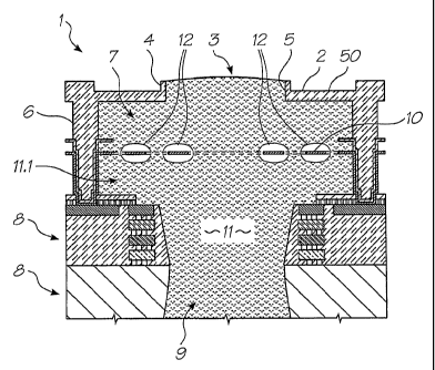
With reference to Figures 1 to 4, the unit cell 1 of a printhead according to
an embodiment
of the invention comprises a nozzle plate 2 with nozzles 3 therein, the
nozzles having
nozzle rims 4, and apertures 5 extending through the nozzle plate. The nozzle
plate 2 is
CA 02506733 2005-05-19
WO 2004/048109 PCT/AU2003/001515
plasma etched from a silicon nitride structure which is deposited, by way of
chemical vapor
deposition (CVD), over a sacrificial material which is subsequently etched.
The printhead also includes, with respect to each nozzle 3, side walls 6 on
which the nozzle
plate is supported, a chamber 7 defined by the walls and the nozzle plate 2, a
mufti-layer
substrate 8 and an inlet passage 9 extending through the mufti-layer substrate
to the far side
(not shown) of the substrate. A looped, elongate heater element 10 is
suspended within the
chamber 7, so that the element is in the form of a suspended beam. The
printhead as shown
is a microelectromechanical system (MEMS) structure, which is formed by a
lithographic
process which is described in more detail below.
When the printhead is in use, ink 11 from a reservoir (not shown) enters the
chamber 7 via
the inlet passage 9, so that the chamber fills to the level as shown in Figure
1. Thereafter,
the heater element 10 is heated for somewhat less than 1 micro second, so that
the heating
is in the form of a thermal pulse. It will be appreciated that the heater
element 10 is in
thermal contact with the ink 11 in the chamber 7 so that when the element is
heated, this
causes the generation of vapor bubbles 12 in the ink. Accordingly, the ink 11
constitutes a
bubble forming liquid. Figure 1 shows the formation of a bubble 12
approximately 1
microsecond after generation of the thermal pulse, that is, when the bubble
has just
nucleated on the heater elements 10. It will be appreciated that, as the heat
is applied in the
form of a pulse, all the energy necessary to generate the bubble 12 is to be
supplied within
that short time.
Turning briefly to Figure 34, there is shown a mask 13 for forming a heater 14
of the
printhead (which heater includes the element 10 referred to above), during a
lithographic
process, as described in more detail below. As the mask 13 is used to form the
heater 14,
the shape of various of its parts correspond to the shape of the element 10.
The mask 13
therefore provides a useful reference by which to identify various parts of
the heater 14.
The heater 14 has electrodes 15 corresponding to the parts designated 15.34 of
the mask 13
and a heater element 10 corresponding to the parts designated 10.34 of the
mask. In
operation, voltage is applied across the electrodes 15 to cause current to
flow through the
element 10. The electrodes 15 are much thicker than the element 10 so that
most of the
electrical resistance is provided by the element. Thus, nearly all of the
power consumed in
CA 02506733 2005-05-19
WO 2004/048109 PCT/AU2003/001515
operating the heater 14 is dissipated via the element 10, in creating the
thermal pulse
referred to above.
When the element 10 is heated as described above, the bubble 12 forms along
the length of
5 the element, this bubble appearing, in the cross-sectional view of Figure 1,
as four bubble
portions, one for each of the element portions shown in cross section.
The bubble 12, once generated, causes an increase in pressure within the
chamber 7, which
in turn causes the ejection of a drop 16 of the ink 11 through the nozzle 3.
The rim 4 assists
10 in directing the drop 16 as it is ejected, so as to minimize the chance of
a drop misdirection.
The reason that there is only one nozzle 3 and chamber 7 per inlet passage 9
is so that the
pressure wave generated within the chamber, on heating of the element 10 and
forming of a
bubble 12, does not effect adjacent chambers and their corresponding nozzles.
The advantages of the heater element 10 being suspended rather than being
embedded in
any solid material, is discussed below.
Figures 2 and 3 show the unit cell 1 at two successive later stages of
operation of the
printhead. It can be seen that the bubble 12 generates further, and hence
grows, with the
resultant advancement of ink 11 through the nozzle 3. The shape of the bubble
12 as it
grows, as shown in Figure 3, is determined by a combination of the inertial
dynamics and
the surface tension of the ink 11. The surface tension tends to minimize the
surface area of
the bubble 12 so that, by the time a certain amount of liquid has evaporated,
the bubble is
essentially disk-shaped.
The increase in pressure within the chamber 7 not only pushes ink 11 out
through the
nozzle 3, but also pushes some ink back through the inlet passage 9. However,
the inlet
passage 9 is approximately 200 to 300 microns in length, and is only
approximately 16
microns in diameter. Hence there is a substantial viscous drag. As a result,
the
predominant effect of the pressure rise in the chamber 7 is to force ink out
through the
nozzle 3 as an ejected drop 16, rather than back through the inlet passage 9.
CA 02506733 2005-05-19
WO 2004/048109 PCT/AU2003/001515
11
Turning now to Figure 4, the printhead is shown at a still further successive
stage of
operation, in which the ink drop 16 that is being ejected is shown during its
"necking
phase" before the drop breaks ofF At this stage, the bubble 12 has already
reached its
maximum size and has then begun to collapse towards the point of collapse 17,
as reflected
in more detail in Figure 5.
The collapsing of the bubble 12 towards the point of collapse 17 causes some
ink 11 to be
drawn from within the nozzle 3 (from the sides 18 of the drop), and some to be
drawn from
the inlet passage 9, towards the point of collapse. Most of the ink 11 drawn
in this manner
is drawn from the nozzle 3, forming an annular neck 19 at the base of the drop
16 prior to
its breaking off.
The drop 16 requires a certain amount of momentum to overcome surface tension
forces, in
order to break off. As ink 11 is drawn from the nozzle 3 by the collapse of
the bubble 12,
the diameter of the neck 19 reduces thereby reducing the amount of total
surface tension
holding the drop, so that the momentum of the drop as it is ejected out of the
nozzle is
sufficient to allow the drop to break off.
When the drop 16 breaks off, cavitation forces are caused as reflected by the
arrows 20, as
the bubble 12 collapses to the point of collapse 17. It will be noted that
there are no solid
surfaces in the vicinity of the point of collapse 17 on which the cavitation
can have an
effect.
Manufacturing process
Relevant parts of the manufacturing process of a printhead according to
embodiments of the
invention are now described with reference to Figures 6 to 29.
Refernng to Figure 6, there is shown a cross-section through a silicon
substrate portion 21,
being a portion of a Memjet printhead, at an intermediate stage in the
production process
thereof. This figure relates to that portion of the printhead corresponding to
a unit cell 1.
The description of the manufacturing process that follows will be in relation
to a unit cell 1,
CA 02506733 2005-05-19
WO 2004/048109 PCT/AU2003/001515
12
although it will be appreciated that the process will be applied to a
multitude of adjacent
unit cells of which the whole printhead is composed.
Figure 6 represents the next successive step, during the manufacturing
process, after the
completion of a standard CMOS fabrication process, including the fabrication
of CMOS
drive transistors (not shown) in the region 22 in the substrate portion 21,
and the
completion of standard CMOS interconnect layers 23 and passivation layer 24.
Wiring
indicated by the dashed lines 25 electrically interconnects the transistors
and other drive
circuitry (also not shown) and the heater element corresponding to the nozzle.
Guard rings 26 are formed in the metallization of the interconnect layers 23
to prevent ink
11 from diffusing from the region, designated 27, where the nozzle of the unit
cell 1 will be
formed, through the substrate portion 21 to the region containing the wiring
25, and
corroding the CMOS circuitry disposed in the region designated 22.
The first stage after the completion of the CMOS fabrication process consists
of etching a
portion of the passivation layer 24 to form the passivation recesses 29.
Figure 8 shows the stage of production after the etching of the interconnect
layers 23, to
form an opening 30. The opening 30 is to constitute the ink inlet passage to
the chamber
that will be formed later in the process.
Figure 10 shows the stage of production after the etching of a hole 31 in the
substrate
portion 21 at a position where the nozzle 3 is to be formed. Later in the
production process,
a further hole (indicated by the dashed line 32) will be etched from the other
side (not
shown) of the substrate portion 21 to join up with the hole 31, to complete
the inlet passage
to the chamber. Thus, the hole 32 will not have to be etched all the way from
the other side
of the substrate portion 21 to the level of the interconnect layers 23.
If, instead, the hole 32 were to be etched all the way to the interconnect
layers 23, then to
avoid the hole 32 being etched so as to destroy the transistors in the region
22, the hole 32
would have to be etched a greater distance away from that region so as to
leave a suitable
margin (indicated by the arrow 34) for etching inaccuracies. But the etching
of the hole 31
CA 02506733 2005-05-19
WO 2004/048109 PCT/AU2003/001515
13
from the top of the substrate portion 21, and the resultant shortened depth of
the hole 32,
means that a lesser margin 34 need be left, and that a substantially higher
packing density
of nozzles can thus be achieved.
Figure 11 shows the stage of production after a four micron thick layer 35 of
a sacrificial
resist has been deposited on the layer 24. This layer 35 fills the hole 31 and
now forms part
of the structure of the printhead. The resist layer 35 is then exposed with
certain patterns (as
represented by the mask shown in Figure 12) to form recesses 36 and a slot 37.
This
provides for the formation of contacts for the electrodes 15 of the heater
element to be
formed later in the production process. The slot 37 will provide, later in the
process, for the
formation of the nozzle walls 6, that will define part of the chamber 7.
Figure 13 shows the stage of production after the deposition, on the layer 35,
of a 0.25
micron thick layer 38 of heater material, which, in the present embodiment, is
of titanium
nitride.
Figure 14 shows the stage of production after patterning and etching of the
heater layer 3 8
to form the heater 14, including the heater element 10 and electrodes 15.
Figure 16 shows the stage of production after another sacrificial resist layer
39, about 1
micron thick, has been added.
Figure 18 shows the stage of production after a second layer 40 of heater
material has been
deposited. In a preferred embodiment, this layer 40, like the first heater
layer 38, is of 0.25
micron thick titanium nitride.
Figure 19 then shows this second layer 40 of heater material after it has been
etched to form
the pattern as shown, indicated by reference numeral 41. In this illustration,
this patterned
layer does not include a heater layer element 10, and in this sense has no
heater
functionality. However, this layer of heater material does assist in reducing
the resistance
of the electrodes 15 of the heater 14 so that, in operation, less energy is
consumed by the
electrodes which allows greater energy consumption by, and therefore greater
effectiveness
CA 02506733 2005-05-19
WO 2004/048109 PCT/AU2003/001515
14
of, the heater elements 10. In the dual heater embodiment illustrated in
Figure 38, the
corresponding layer 40 does contain a heater 14.
Figure 21 shows the stage of production after a third layer 42, of sacrificial
resist, has been
deposited. As the uppermost level of this layer will constitute the inner
surface of the
nozzle plate 2 to be formed later, and hence the inner extent of the nozzle
aperture 5, the
height of this layer 42 must be sufficient to allow for the formation of a
bubble 12 in the
region designated 43 during operation of the printhead.
Figure 23 shows the stage of production after the roof layer 44 has been
deposited, that is,
the layer which will constitute the nozzle plate 2. Instead of being formed
from 100 micron
thick polyimide film, the nozzle plate 2 is formed of silicon nitride, just 2
microns thick.
Figure 24 shows the stage of production after the chemical vapor deposition
(CVD) of
silicon nitride forming the layer 44, has been partly etched at the position
designated 45, so
as to form the outside part of the nozzle rim 4, this outside part being
designated 4.1
Figure 26 shows the stage of production after the CVD of silicon nitride has
been etched all
the way through at 46, to complete the formation of the nozzle rim 4 and to
form the nozzle
aperture 5, and after the CVI~ silicon nitride has been removed at the
position designated 47
where it is not required.
Figure 28 shows the stage of production after a protective layer 48 of resist
has been
applied. After this stage, the substrate portion 21 is then ground from its
other side (not
shown) to reduce the substrate portion from its nominal thickness of about 800
microns to
about 200 microns, and then, as foreshadowed above, to etch the hole 32. The
hole 32 is
etched to a depth such that it meets the hole 31.
Then, the sacrificial resist of each of the resist layers 35, 39, 42 and 48,
is removed using
oxygen plasma, to form the structure shown in Figure 30, with walls 6 and
nozzle plate 2
which together define the chamber 7 (part of the walls and nozzle plate being
shown cut-
away). It will be noted that this also serves to remove the resist filling the
hole 31 so that
this hole, together with the hole 32 (not shown in figure 30), define a
passage extending
CA 02506733 2005-05-19
WO 2004/048109 PCT/AU2003/001515
from the lower side of the substrate portion 21 to the nozzle 3, this passage
serving as the
ink inlet passage, generally designated 9, to the chamber 7.
While the above production process is used to produce the embodiment of the
printhead
5 shown in Figure 30, further printhead embodiments, having different heater
structures, are
shown in Figure 33, Figures 35 and 37, and Figures 38 and 40.
Coht~ol of ink drop ejection
10 Referring once again to Figure 30, the unit cell 1 shown, as mentioned
above, is shown with
part of the walls 6 and nozzle plate 2 cut-away, which reveals the interior of
the chamber 7.
The heater 14 is not shown cut away, so that both halves of the heater element
10 can be
seen.
15 In operation, ink 11 passes through the ink inlet passage 9 (see Figure 28)
to fill the
chamber 7. Then a voltage is applied across the electrodes 15 to establish a
flow of electric
current through the heater element 10. This heats the element 10, as described
above in
relation to Figure 1, to form a vapor bubble in the ink within the chamber 7.
The various possible structures for the heater 14, some of which are shown in
Figures 33,
35 and 37, and 38, can result in there being many variations in the ratio of
length to width
of the heater elements 10. Such variations (even though the surface area of
the elements 10
may be the same) may have significant effects on the electrical resistance of
the elements,
and therefore on the balance between the voltage and current to achieve a
certain power of
the element.
Modern drive electronic components tend to require lower drive voltages than
earlier
versions, with lower resistances of drive transistors in their "on" state.
Thus, in such drive
transistors, for a given transistor area, there is a tendency to higher
current capability and
lower voltage tolerance in each process generation.
Figure 36, referred to above, shows the shape, in plan view, of a mask for
forming the
heater structure of the embodiment of the printhead shown in Figure 35.
Accordingly, as
CA 02506733 2005-05-19
WO 2004/048109 PCT/AU2003/001515
16
Figure 36 represents the shape of the heater element 10 of that embodiment, it
is now
referred to in discussing that heater element. During operation, current flows
vertically into
the electrodes 15 (represented by the parts designated 15.36), so that the
current flow area
of the electrodes is relatively large, which, in turn, results in there being
a low electrical
resistance. By contrast, the element 10, represented in figure 36 by the part
designated
10.36, is long and thin, with the width of the element in this embodiment
being 1 micron a
and the thickness being 0.25 microns.
It will be noted that the heater 14 shown in Figure 33 has a significantly
smaller element 10
than the element 10 shown in Figure 35, and has just a single loop 36.
Accordingly, the
element 10 of Figure 33 will have a much lower electrical resistance, and will
permit a
higher current flow, than the element 10 of Figure 35. It therefore requires a
lower drive
voltage to deliver a given energy to the heater 14 in a given time.
In Figure 38, on the other hand, the embodiment shown includes a heater 14
having two
heater elements 10.1 and 10.2 corresponding to the same unit cell 1. One of
these elements
10.2 is twice the width as the other element 10.1, with a correspondingly
larger surface
area. The various paths of the lower element 10.2 are 2 microns in width,
while those of the
upper element 10.1 are 1 micron in width. Thus the energy applied to ink in
the chamber 7
by the lower element 10.2 is twice that applied by the upper element 10.1 at a
given drive
voltage and pulse duration. This permits a regulating of the size of vapor
bubbles and
hence of the size of ink drop ejected due to the bubbles.
Assuming that the energy applied to the ink by the upper element 10.1 is X, it
will be
appreciated that the energy applied by the lower element 10.2 is about 2X, and
the energy
applied by the two elements together is about 3X. Of course, the energy
applied when
neither element is operational, is zero. Thus, in effect, two bits of
information can be
printed with the one nozzle 3.
As the above factors of energy output may not be achieved exactly in practice,
some "fine
tuning" of the exact sizing of the elements 10.1 and 10.2, or of the drive
voltages that are
applied to them, may be required.
CA 02506733 2005-05-19
WO 2004/048109 PCT/AU2003/001515
17
It will also be noted that the upper element 10.1 is rotated through
180° about a vertical axis
relative to the lower element 10.2. This is so that their electrodes 15 are
not coincident,
allowing independent connection to separate drive circuits.
Features and advantages of particular embodiments
Discussed below, under appropriate headings, are certain specific features of
embodiments
of the invention, and the advantages of these features. The features are to be
considered in
relation to all of the drawings pertaining to the present invention unless the
context
specifically excludes certain drawings, and relates to those drawings
specifically referred
to.
Suspended beam heater
With reference to Figure 1, and as mentioned above, the heater element 10 is
in the form of
a suspended beam, and this is suspended over at least a portion (designated
11.1) of the ink
11 (bubble forming liquid). The element 10 is configured in this way rather
than forming
part of, or being embedded in, a substrate as is the case in existing
printhead systems made
by various manufacturers such as Hewlett Packard, Canon and Lexmark. This
constitutes a
significant difference between embodiments of the present invention and the
prior ink jet
technologies.
The main advantage of this feature is that a higher efficiency can be achieved
by avoiding
the unnecessary heating of the solid material that surrounds the heater
elements 10 (for
example the solid material forming the chamber walls 6, and surrounding the
inlet passage
9) which takes place in the prior art devices. The heating of such solid
material does not
contribute to the formation of vapor bubbles 12, so that the heating of such
material
involves the wastage of energy. The only energy which contributes in any
significant sense
to the generation of the bubbles 12 is that which is applied directly into the
liquid which is
to be heated, which liquid is typically the ink 11.
In one preferred embodiment, as illustrated in Figure 1, the heater element 10
is suspended
within the ink 11 (bubble forming liquid), so that this liquid surrounds the
element. This is
CA 02506733 2005-05-19
WO 2004/048109 PCT/AU2003/001515
18
further illustrated in Figure 41. In another possible embodiment, as
illustrated in Figure 42,
the heater element 10 beam is suspended at the surface of the ink (bubble
forming liquid)
1 l, so that this liquid is only below the element rather than surrounding it,
and there is air
on the upper side of the element. The embodiment described in relation to
Figure 41 is
preferred as the bubble 12 will form all around the element 10 unlike in the
embodiment
described in relation to Figure 42 where the bubble will only form below the
element. Thus
the embodiment of Figure 41 is likely to provide a more efficient operation.
As can be seen in, for example, with reference to Figures 30 and 31, the
heater element 10
beam is supported only on one side and is free at its opposite side, so that
it constitutes a
cantilever.
Efficiency of the printhead
The feature presently under consideration is that the heater element 10 is
configured such
that an energy of less than 500 nanojoules (nJ) is required to be applied to
the element to
heat it sufficiently to form a bubble ~12 in the ink 11, so as to eject a drop
16 of ink through
a nozzle 3. In one preferred embodiment, the required energy is less that 300
nJ, while in a
further embodiment, the energy is less than 120 nJ.
It will be appreciated by those skilled in the art that prior art devices
generally require over
5 microjoules to heat the element sufficiently to generate a vapor bubble 12
to eject an ink
drop 16. Thus, the energy requirements of the present invention are an order
of magnitude
lower than that of known thermal ink jet systems. This lower energy
consumption allows
lower operating costs, smaller power supplies, and so on, but also
dramatically simplifies
printhead cooling, allows higher densities of nozzles 3, and permits printing
at higher
resolutions.
These advantages of the present invention are especially significant in
embodiments where
the individual ejected ink drops 16, themselves, constitute the major cooling
mechanism of
the printhead, as described further below.
CA 02506733 2005-05-19
WO 2004/048109 PCT/AU2003/001515
19
Self coolie og f the printhead
This feature of the invention provides that the energy applied to a heater
element 10 to form
a vapor bubble 12 so as to eject a drop 16 of ink 11 is removed from the
printhead by a
combination of the heat removed by the ejected drop itself, and the ink that
is taken into the
printhead from the ink reservoir (not shown). The result of this is that the
net "movement"
of heat will be outwards from the printhead, to provide for automatic cooling.
Under these
circumstances, the printhead does not require any other cooling systems.
As the ink drop 16 ejected and the amount of ink 11 drawn into the printhead
to replace the
ejected drop are constituted by the same type of liquid, and will essentially
be of the same
mass, it is convenient to express the net movement of energy as, on the one
hand, the
energy added by the heating of the element 10, and on the other hand, the net
removal of
heat energy that results from ejecting the ink drop 16 and the intake of the
replacement
quantity of ink 11. Assuming that the replacement quantity of ink 11 is at
ambient
temperature, the change in energy due to net movement of the ejected and
replacement
quantities of ink can conveniently be expressed as the heat that would be
required to raise
the temperature of the ejected drop 16, if it were at ambient temperature, to
the actual
temperature of the drop as it is ejected.
It will be appreciated that a determination of whether the above criteria are
met depends on
what constitutes the ambient temperature. In the present case, the temperature
that is taken
to be the ambient temperature is the temperature at which ink 11 enters the
printhead from
the ink storage reservoir (not shown) which is connected, in fluid flow
communication, to
the inlet passages 9 of the printhead. Typically the ambient temperature will
be the room
ambient temperature, which is usually roughly 20 degrees C (Celsius).
However, the ambient temperature may be less, if for example, the room
temperature is
lower, or if the ink 11 entering the printhead is refrigerated.
In one preferred embodiment, the printhead is designed to achieve complete
self cooling
(i.e. where the outgoing heat energy due to the net effect of the ejected and
replacement
quantities of ink 11 is equal to the heat energy added by the heater element
10).
CA 02506733 2005-05-19
WO 2004/048109 PCT/AU2003/001515
By way of example, assuming that the ink 11 is the bubble forming liquid and
is water
based, thus having a boiling point of approximately 100 degrees C, and if the
ambient
temperature is 40 degrees C, then there is a maximum of 60 degrees C from the
ambient
5 temperature to the ink boiling temperature and that is the maximum
temperature rise that
the printhead could undergo.
It is desirable to avoid having ink temperatures within the printhead (other
than at time of
ink drop 16 ejection) which are very close to the boiling point of the ink 11.
If the ink 11
10 were at such a temperature, then temperature variations between parts of
the printhead
could result in some regions being above boiling point, with the unintended,
and therefore
undesirable, formation of vapor bubbles 12. Accordingly, a preferred
embodiment of the
invention is configured such that complete self cooling, as described above,
can be
achieved when the maximum temperature of the ink 11 (bubble forming liquid) in
a
15 particular nozzle chamber 7 is 10 degrees C below its boiling point when
the heating
element 10 is not active.
The main advantage of the feature presently under discussion, and its various
embodiments,
is that it allows for a high nozzle density and for a high speed of printhead
operation
20 without requiring elaborate cooling methods for preventing undesired
boiling in nozzles 3
adjacent to nozzles from which ink drops 16 are being ejected. This can allow
as much as a
hundred-fold increase in nozzle packing density than would be the case if such
a feature,
and the temperature criteria mentioned, were not present.
Areal density of nozzles
This feature of the invention relates to the density, by area, of the nozzles
3 on the
printhead. With reference to Figure 1, the nozzle plate 2 has an upper surface
50, and the
present aspect of the invention relates to the packing density of nozzles 3 on
that surface.
More specifically, the areal density of the nozzles 3 on that surface 50 is
over 10,000
nozzles per square cm of surface area.
CA 02506733 2005-05-19
WO 2004/048109 PCT/AU2003/001515
21
In one preferred embodiment, the areal density exceeds 20,000 nozzles 3 per
square cm of
surface 50 area, while in another preferred embodiment, the areal density
exceeds 40,000
nozzles 3 per square cm. In a preferred embodiment, the areal density is 48
828 nozzles 3
per square cm.
When referring to the areal density, each nozzle 3 is taken to include the
drive-circuitry
corresponding to the nozzle, which consists, typically, of a drive transistor,
a shift register,
an enable gate and clock regeneration circuitry (this circuitry not being
specifically
identified).
With reference to Figure 43 in which a single unit cell 1 is shown, the
dimensions of the
unit cell are shown as being 32 microns in width by 64 microns in .r~~gt~~.
The nozzle 3 of
the next successive row of nozzles (not shown) immediately juxtaposes this
nozzle, so that,
as a result of the dimension of the outer periphery of the printhead chip,
there are 48,828
nozzles 3 per square cm. This is about 85 times the nozzle areal density of a
typical
thermal ink jet printhead, and roughly 400 times the nozzle areal density of a
piezoelectric
printhead.
The main advantage of a high areal density is low manufacturing cost, as the
devices are
batch fabricated on silicon wafers of a particular size.
The more nozzles 3 that can be accommodated in a square cm of substrate, the
more
nozzles can be fabricated in a single batch, which typically consists of one
wafer. The cost
of manufacturing a CMOS plus MEMS wafer of the type used in the printhead of
the
present invention is, to a some extent, independent of the nature of patterns
that are formed
on it. Therefore if the patterns are relatively small, a relatively large
number of nozzles 3
can be included. This allows more nozzles 3 and more printheads to be
manufactured for
the same cost than in a cases where the nozzles had a lower areal density. The
cost is
directly proportional to the area taken by the nozzles 3.
Bubble formation on obposite sides of heater element
CA 02506733 2005-05-19
WO 2004/048109 PCT/AU2003/001515
22
According to the present feature, the heater 14 is configured so that when a
bubble 12 forms
in the ink 11 (bubble forming liquid), it forms on both sides of the heater
element 10.
Preferably, it forms so as to surround the heater element 10 where the element
is in the
form of a suspended beam.
The formation of a bubble 12 on both sides of the heater element 10 as opposed
to on one
side only, can be understood with reference to Figures 45 and 46. In the first
of these
figures, the heater element 10 is adapted for the bubble 12 to be formed only
on one side as,
while in the second of these figures, the element is adapted for the bubble 12
to be formed
on both sides, as shown.
In a configuration such as that of Figure 45, the reason that the bubble 12
forms on only one
side of the heater element 10 is because the element is embedded in a
substrate 51, so that
the bubble cannot be formed on the particular side corresponding to the
substrate. By
contrast, the bubble 12 can form on both sides in the configuration of Figure
46 as the
heater element 10 here is suspended.
Of course where the heater element 10 is in the form of a suspended beam as
described
above in relation to Figure 1, the bubble 12 is allowed to form so as to
surround the
suspended beam element.
The advantage of the bubble 12 forming on both sides is the higher efficiency
that is
achievable. This is due to a reduction in heat that is wasted in heating solid
materials in the
vicinity of the heater element 10, which do not contribute to formation of a
bubble 12. This
is illustrated in Figure 45, where the arrows 52 indicate the movements of
heat into the
solid substrate 51. The amount of heat lost to the substrate 51 depends on the
thermal
conductivity of the solid materials of the substrate relative to that of the
ink 11, which may
be water based. As the thermal conductivity of water is relatively low, more
than half of
the heat can be expected to be absorbed by the substrate 51 rather than by the
ink 11.
Prevention of cavitation
CA 02506733 2005-05-19
WO 2004/048109 PCT/AU2003/001515
23
As described above, after a bubble 12 has been formed in a printhead according
to an
embodiment of the present invention, the bubble collapses towards a point of
collapse 17.
According to the feature presently being addressed, the heater elements 10 are
configured
to form the bubbles 12 so that the points of collapse 17 towards which the
bubbles collapse,
are at positions spaced from the heater elements. Preferably, the printhead is
configured so
that there is no solid material at such points of collapse 17. In this way
cavitation, being a
major problem in prior art thermal ink jet devices, is largely eliminated.
Referring to Figure 48, in a preferred embodiment, the heater elements 10 are
configured to
have parts 53 which define gaps (represented by the arrow 54), and to form the
bubbles 12
so that the points of collapse 17 to which the bubbles collapse are located at
such gaps. The
advantage of this feature is that it substantially avoids cavitation damage to
the heater
elements 10 and other solid material.
In a standard prior art system as shown schematically in Figure 47, the heater
element 10 is
embedded in a substrate 55, with an insulating layer 56 over the element, and
a protective
layer 57 over the insulating layer. When a bubble 12 is formed by the element
10, it is
formed on top of the element. When the bubble 12 collapses, as shown by the
arrows 58,
all of the energy of the bubble collapse is focussed onto a very small point
of collapse 17.
If the protective layer 57 were absent, then the mechanical forces due to the
cavitation that
would result from the focussing of this energy to the point of collapse 17,
could chip away
or erode the heater element 10. However, this is prevented by the protective
layer 57.
Typically, such a protective layer 57 is of tantalum, which oxidizes to form a
very hard
layer of tantalum pentoxide (Ta205). Although no known materials can fully
resist the
effects of cavitation, if the tantalum pentoxide should be chipped away due to
the
cavitation, then oxidation will again occur at the underlying tantalum metal,
so as to
effectively repair the tantalum pentoxide layer.
Although the tantalum pentoxide functions relatively well in this regard in
known thermal
ink jet systems, it has certain disadvantages. One significant disadvantage is
that, in effect,
virtually the whole protective layer 57 (having a thickness indicated by the
reference
numeral 59) must be heated in order to transfer the required energy into the
ink 11, to heat
CA 02506733 2005-05-19
WO 2004/048109 PCT/AU2003/001515
24
it so as to form a bubble 12. This layer 57 has a high thermal mass due to the
very high
atomic weight of the tantalum, and this reduces the efficiency of the heat
transfer. Not only
does this increase the amount of heat which is required at the level
designated 59 to raise
the temperature at the level designated 60 sufficiently to heat the ink 11,
but it also results
in a substantial thermal loss to take place in the directions indicated by the
arrows 61.
These disadvantage would not be present if the heater element 10 was merely
supported on
a surface and was not covered by the protective layer 57.
According to the feature presently under discussion, the need for a protective
layer 57, as
described above, is avoided by generating the bubble 12 so that it collapses,
as illustrated in
Figure 48, towards a point of collapse 17 at which there is no solid material,
and more
particularly where there is the gap 54 between parts 53 of the heater element
10. As there is
merely the ink 11 itself in this location (prior to bubble generation), there
is no material that
can be eroded here by the effects of cavitation. The temperature at the point
of collapse 17
may reach many thousands of degrees C, as is demonstrated by the phenomenon of
sonoluminesence. This will break down the ink components at that point.
However, the
volume of extreme temperature at the point of collapse 17 is so small that the
destruction of
ink components in this volume is not significant.
The generation of the bubble 12 so that it collapses towards a point of
collapse 17 where
there is no solid material can be achieved using heater elements 10
corresponding to that
represented by the part 10.34 of the mask shown in Figure 34. The element
represented is
symmetrical, and has a hole represented by the reference numeral 63 at its
center. When
the element is heated, the bubble forms around the element (as indicated by
the dashed line
64) and then grows so that, instead of being of annular (doughnut) shape as
illustrated by
the dashed lines 64 and 65) it spans the element including the hole 63, the
hole then being
filled with the vapor that forms the bubble. The bubble 12 is thus
substantially disc-shaped.
When it collapses, the collapse is directed so as to minimize the surface
tension surrounding
the bubble 12. This involves the bubble shape moving towards a spherical shape
as far as is
permitted by the dynamics that are involved. This, in turn, results in the
point of collapse
being in the region of the hole 63 at the center of the heater element 10,
where there is no
solid material.
CA 02506733 2005-05-19
WO 2004/048109 PCT/AU2003/001515
The heater element 10 represented by the part 10.31 of the mask shown in
Figure 31 is
configured to achieve a similar result, with the bubble generating as
indicated by the dashed
line 66, and the point of collapse to which the bubble collapses being in the
hole 67 at the
center of the element.
5
The heater element 10 represented as the part 10.36 of the mask shown in
Figure 36 is also
configured to achieve a similar result. Where the element 10.36 is dimensioned
such that
the hole 68 is small, manufacturing inaccuracies of the heater element may
affect the extent
to which a bubble can be formed such that its point of collapse is in the
region defined by
10 the hole. For example, the hole may be as little as a few microns across.
Where high levels
of accuracy in the element 10.36 cannot be achieved, this may result in
bubbles represented
as 12.36 that are somewhat lopsided, so that they cannot be directed towards a
point of
collapse within such a small region. In such a case, with regard to the heater
element
represented in Figure 36, the central loop 49 of the element can simply be
omitted, thereby
15 increasing the size of the region in which the point of collapse of the
bubble is to fall.
Chemical vapor deposited nozzle plate, and thin nozzle plates
The nozzle aperture 5 of each unit cell 1 extends through the nozzle plate 2,
the nozzle plate
20 thus constituting a structure which is formed by chemical vapor deposition
(CVD). In
various preferred embodiments, the CVD is of silicon nitride, silicon dioxide
or oxi-nitride.
The advantage of the nozzle plate 2 being formed by CVD is that it is formed
in place
without the requirement for assembling the nozzle plate to other components
such as the
25 walls 6 of the unit cell 1. This is an important advantage because the
assembly of the nozzle
plate 2 that would otherwise be required can be difficult to effect and can
involve
potentially complex issues. Such issues include the potential mismatch of
thermal
expansion between the nozzle plate 2 and the parts to which it would be
assembled, the
difficulty of successfully keeping components aligned to each other, keeping
them planar,
and so on, during the curing process of the adhesive which bonds the nozzle
plate 2 to the
other parts.
CA 02506733 2005-05-19
WO 2004/048109 PCT/AU2003/001515
26
The issue of thermal expansion is a significant factor in the prior art, which
limits the size
of ink jets that can be manufactured. This is because the difference in the
coefficient of
thermal expansion between, for example, a nickel nozzle plate and a substrate
to which the
nozzle plate is connected, where this substrate is of silicon, is quite
substantial.
Consequently, over as small a distance as that occupied by, say, 1000 nozzles,
the relative
thermal expansion that occurs between the respective parts, in being heated
from the
ambient temperature to the curing temperature required for bonding the parts
together, can
cause a dimension mismatch of significantly greater than a whole nozzle
length. This
would be significantly detrimental for such devices.
Another problem addressed by the features of the invention presently under
discussion, at
least in embodiments thereof, is that, in prior art devices, nozzle plates
that need to be
assembled are generally laminated onto the remainder of the printhead under
conditions of
relatively high stress. This can result in breakages or undesirable
deformations of the
devices. The depositing of the nozzle plate 2 by CVD in embodiments of the
present
invention avoids this.
A further advantage of the present features of the invention, at least in
embodiments
thereof, is their compatibility with existing semiconductor manufacturing
processes.
Depositing a nozzle plate 2 by CVD allows the nozzle plate to be included in
the printhead
at the scale of normal silicon wafer production, using processes normally used
for semi-
conductor manufacture.
Existing thermal ink jet or bubble jet systems experience pressure transients,
during the
bubble generation phase, of up to 100 atmospheres. If the nozzle plates 2 in
such devices
were applied by CVD, then to withstand such pressure transients, a substantial
thickness of
CVD nozzle plate would be required. As would be understood by those skilled in
the art,
such thicknesses of deposited nozzle plates would give rise certain problems
as discussed
below.
For example, the thickness of nitride sufficient to withstand a 100 atmosphere
pressure in
the nozzle chamber 7 may be, say, 10 microns. With reference to Figure 49,
which shows a
unit cell 1 that is not in accordance with the present invention, and which
has such a thick
CA 02506733 2005-05-19
WO 2004/048109 PCT/AU2003/001515
27
nozzle plate 2, it will be appreciated that such a thickness can result in
problems relating to
drop ejection. In this case, due to the thickness of nozzle plate 2, the
fluidic drag exerted by
the nozzle 3 as the ink 11 is ejected therethrough results in significant
losses in the
efficiency of the device.
Another problem that would exist in the case of such a thick nozzle plate 2,
relates to the
actual etching process. This is assuming that the nozzle 3 is etched, as
shown, perpendicular
to the wafer 8 of the substrate portion, for example using a standard plasma
etching. This
would typically require more than 10 microns of resist 69 to be applied. To
expose that
thickness of resist 69, the required level of resolution becomes difficult to
achieve, as the
focal depth of the stepper that is used to expose the resist is relatively
small. Although it
would be possible to expose this relevant depth of resist 69 using x-rays,
this would be a
relatively costly process.
A further problem that would exist with such a thick nozzle plate 2 in a case
where a 10
micron thick layer of nitride were CVD deposited on a silicon substrate wafer,
is that,
because of the difference in thermal expansion between the CVD layer and the
substrate, as
well as the inherent stress of within thick deposited layer, the wafer could
be caused to bow
to such a degree that further steps in the lithographic process would become
impractical.
Thus, a layer for the nozzle plate 2 as thick as 10 microns (unlike in the
present invention),
while possible, is disadvantageous.
With reference to Figure 50, in a Memjet thermal ink ejection device according
to an
embodiment of the present invention, the CVD nitride nozzle plate layer 2 is
only 2
microns thick. Therefore the fluidic drag through the nozzle 3 is not
particularly significant
and is therefore not a major cause of loss.
Furthermore, the etch time, and the resist thickness required to etch nozzles
3 in such a
nozzle plate 2, and the stress on the substrate wafer 8, will not be
excessive.
The relatively thin nozzle plate 2 in this invention is enabled as the
pressure generated in
the chamber 7 is only approximately 1 atmosphere and not 100 atmospheres as in
prior art
devices, as mentioned above.
CA 02506733 2005-05-19
WO 2004/048109 PCT/AU2003/001515
28
There are many factors which contribute to the significant reduction in
pressure transient
required to eject drops 16 in this system. These include:
1. small size of chamber 7;
2. accurate fabrication of nozzle 3 and chamber 7;
3. stability of drop ejection at low drop velocities;
4. very low fluidic and thermal crosstalk between nozzles 3;
5. optimum nozzle size to bubble area;
6. low fluidic drag through thin (2 micron) nozzle 3;
7. low pressure loss due to ink ejection through the inlet 9;
~. self cooling operation.
As mentioned above in relation the process described in terms of Figures 6 to
31, the
etching of the 2-micron thick nozzle plate layer 2 involves two relevant
stages. One such
stage involves the etching of the region designated 45 in Figures 24 and 50,
to form a recess
outside of what will become the nozzle rim 4. The other such stage involves a
further etch,
in the region designated 46 in Figures 26 and 50, which actually forms the
nozzle~aperture 5
and finishes the rim 4.
Nozzle plate thicknesses
As addressed above in relation to the formation of the nozzle plate 2 by CVD,
and with the
advantages described in that regard, the nozzle plates in the present
invention are thinner
than in the prior art. More particularly, the nozzle plates 2 are less than 10
microns thick.
In one preferred embodiment, the nozzle plate 2 of each unit cell 1 is less
than 5 microns
thick, while in another preferred embodiment, it is less than 2.5 microns
thick. Indeed, a
preferred thickness for the nozzle plate 2 is 2 microns thick.
Heater elements formed in different la,
According to the present feature, there are a plurality of heater elements 10
disposed within
the chamber 7 of each unit cell 1. The elements 10, which are formed by the
lithographic
process as described above in relation to Figure 6 to 31, are formed in
respective layers.
CA 02506733 2005-05-19
WO 2004/048109 PCT/AU2003/001515
29
In preferred embodiments, as shown in Figures 38, 40 and 51, the heater
elements 10.1 and
10.2 in the chamber 7, axe of different sizes relative to each other.
Also as will be appreciated with reference to the above description of the
lithographic
process, each heater element 10.1, 10.2 is formed by at least one step of that
process, the
lithographic steps relating to each one of the elements 10.1 being distinct
from those
relating to the other element 10.2.
The elements 10.1, 10.2 are preferably sized relative to each other, as
reflected
schematically in the diagram of Figure 51, such that they can achieve binary
weighted ink
drop volumes, that is, so that they can cause ink drops 16 having different,
binary weighted
volumes to be ejected through the nozzle 3 of the particular unit cell 1. The
achievement of
the binary weighting of the volumes of the ink drops 16 is determined by the
relative sizes
of the elements 10.1 and 10.2. In Figure 51, the area of the bottom heater
element 10.2 in
contact with the ink 11 is twice that of top heater element 10.1.
One known prior art device, patented by Canon, and illustrated schematically
in Figure 52,
also has two heater elements 10.1 and 10.2 for each nozzle, and these are also
sized on a
binary basis (i.e. to produce drops 16 with binary weighted volumes). These
elements 10.1,
10.2 are formed in a single layer, adjacent to each other in the nozzle
chamber 7. It will be
appreciated that the bubble 12.1 formed by the small element 10.1, only, is
relatively small,
while that 12.2 formed by the large element 10.2, only, is relatively large.
The bubble
generated by the combined effects of the two elements, when they are actuated
simultaneously, is designated 12.3. Three differently sized ink drops 16 will
be caused to
be ejected by the three respective bubbles 12.1, 12.2 and 12.3.
It will be appreciated that the size of the elements 10.1 and 10.2 themselves
are not required
to be binary weighted to cause the ejection of drops 16 having different sizes
or the ejection
of useful combinations of drops. Indeed, the binary weighting may well not be
represented
precisely by the area of the elements 10.1, 10.2 themselves. In sizing the
elements 10.1,
10.2 to achieve binary weighted drop volumes, the fluidic characteristics
surrounding the
generation of bubbles 12, the drop dynamics characteristics, the quantity of
liquid that is
CA 02506733 2005-05-19
WO 2004/048109 PCT/AU2003/001515
drawing back into the chamber 7 from the nozzle 3 once a drop 16 has broken
off, and so
forth, must be considered. Accordingly, the actual ratio of the surface areas
of the elements
10.1, 10.2, or the performance of the two heaters, needs to be adjusted in
practice to achieve
the desired binary weighted drop volumes.
5
Where the size of the heater elements 10.1, 10.2 is fixed and where the ratio
of their surface
areas is therefore fixed, the relative sizes of ejected drops 16 may be
adjusted by adjusting
the supply voltages to the two elements. This can also be achieved by
adjusting the
duration of the operation pulses of the elements 10.1, 10.2 - i.e. their pulse
widths.
10 However, the pulse widths cannot exceed a certain amount of time, because
once a bubble
12 has nucleated on the surface of an element 10.1, 10.2, then any duration of
pulse width
after that time will be of little or no effect.
On the other hand, the low thermal mass of the heater elements 10.1, 10.2
allows them to be
15 heated to reach, very quickly, the temperature at which bubbles 12 are
formed and at which
drops 16 are ejected. While the maximum effective pulse width is limited, by
the onset of
bubble nucleation, typically to around 0.5 microseconds, the minimum pulse
width is
limited only by the available current drive and the current density that can
be tolerated by
the heater elements 10.1, 10.2. .
As shown in Figure 51, the two heaters elements 10.1, 10.2 are connected to
two respective
drive circuits 70. Although these circuits 70 may be identical to each other,
a further
adjustment can be effected by way of these circuits, for example by sizing the
drive
transistor (not shown) connected to the lower element 10.2, which is the high
current
element, larger than that connected to the upper element 10.1. If, for
example, the relative
currents provided to the respective elements 10.1, 10.2 are in the ratio 2:1,
the drive
transistor of the circuit 70 connected to the lower element 10.2 would
typically be twice the
width of the drive transistor (also no shown) of the circuit 70 connected to
the other
element 10.1.
In the prior art described in relation to Figure 52, the heater elements 10.1,
10.2, which are
in the same layer, are produced simultaneously in the same step of the
lithographic
manufacturing process. In the embodiment of the present invention illustrated
in Figure 51,
CA 02506733 2005-05-19
WO 2004/048109 PCT/AU2003/001515
31
the two heaters elements 10.1, 10.2, as mentioned above, are formed one after
the other.
Indeed, as described in the process illustrated with reference to Figures 6 to
31, the material
to form the element 10.2 is deposited and is then etched in the lithographic
process,
whereafter a sacrificial layer 39 is deposited on top of that element, and
then the material
for the other element 10.1 is deposited so that the sacrificial layer is
between the two heater
element layers. The layer of the second element 10.1 is etched by a second
lithographic
step, and the sacrificial layer 39 is removed.
Referring once again to the different sizes of the heater elements 10.1 and
10.2, as
mentioned above, this has the advantage that it enables the elements to be
sized so as to
achieve multiple, binary weighted drop volumes from one nozzle 3.
It will be appreciated that, where multiple drop volumes can be achieved, and
especially if
they are binary weighted, then photographic quality can be obtained while
using fewer
printed dots, and at a lower print resolution.
Furthermore, under the same circumstances, higher speed printing can be
achieved. That is,
instead of just ejecting one drop 14 and then waiting for the nozzle 3 to
refill, the equivalent
of one, two, or three drops might be ejected. Assuming that the available
refill speed of the
nozzle 3 is not a limiting factor, ink ejection, and hence printing, up to
three times faster,
may be achieved. In practice, however, the nozzle refill time will typically
be a limiting
factor. In this case, the nozzle 3 will take slightly longer to refill when a
triple volume of
drop 16 (relative to the minimum size drop) has been ejected than when only a
minimum
volume drop has been ejected. However, in practice it will not take as much as
three times
as long to refill. This is due to the inertial dynamics and the surface
tension of the ink 11.
Referring to Figure 53, there is shown, schematically, a pair of adjacent unit
cells 1.1 and
1.2, the cell on the left 1.1 representing the nozzle 3 after a larger volume
of drop 16 has
been ejected, and that on the right 1.2, after a drop of smaller volume has
been ejected. In
the case of the larger drop 16, the curvature of the air bubble 71 that has
formed inside the
partially emptied nozzle 3.1 is larger than in the case of air bubble 72 that
has formed after
the smaller volume drop has been ejected from the nozzle 3.2 of the other unit
cell 1.2.
CA 02506733 2005-05-19
WO 2004/048109 PCT/AU2003/001515
32
The higher curvature of the air bubble 71 in the unit cell 1.1 results in a
greater surface
tension force which tends to draw the ink 11, from the refill passage 9
towards the nozzle 3
and into the chamber 7.1, as indicated by the arrow 73. This gives rise to a
shorter refilling
time. As the chamber 7.1 refills, it reaches a stage, designated 74, where the
condition is
similar to that in the adjacent unit cell 1.2. In this condition, the chamber
7.1 of the unit cell
1.1 is partially refilled and the surface tension force has therefore reduced.
This results in
the refill speed slowing down even though, at this stage, when this condition
is reached in
that unit cell 1.1, a flow of liquid into the chamber 7.l,with its associated
momentum, has
been established. The overall effect of this is that, although it takes longer
to completely
fill the chamber 7.1 and nozzle 3.1 from a time when the air bubble 71 is
present than from
when the condition 74 is present, even if the volume to be refilled is three
times larger, it
does not take as much as three times longer to refill the chamber 7.1 and
nozzle 3.1.
Heater elements formed from materials constituted by elements with low atomic-
numbers
This feature involves the heater elements 10 being formed of solid material,
at least 90% of
which, by weight, is constituted by one or more periodic elements having an
atomic number
below 50. In a preferred embodiment the atomic weight is below 30, while in
another
embodiment the atomic weight is below 23.
The advantage of a low atomic number is that the atoms of that material have a
lower mass,
and therefore less energy is required to raise the temperature of the heater
elements 10.
This is because, as will be understood by those skilled in the art, the
temperature of an
article is essentially related to the state of movement of the nuclei of the
atoms.
Accordingly, it will require more energy to raise the temperature, and thereby
induce such a
nucleus movement, in a material with atoms having heavier nuclei that in a
material having
atoms with lighter nuclei.
Materials currently used for the heater elements of thermal ink jet systems
include tantalum
aluminum alloy (for example used by Hewlett Packard), and hafnium boride (for
example
used by Canon). Tantalum and hafnium have atomic numbers 73 and 72,
respectively,
while the material used in the Memjet heater elements 10 of the present
invention is
titanium nitride. Titanium has an atomic number of 22 and nitrogen has an
atomic number
CA 02506733 2005-05-19
WO 2004/048109 PCT/AU2003/001515
33
of 7, these materials therefore being significantly lighter than those of the
relevant prior art
device materials.
Boron and aluminum, which form part of hafnium boride and tantalum aluminum,
respectively, like nitrogen, are relatively light materials. However, the
density of tantalum
nitride is 16.3 glcm3, while that of titanium nitride (which includes titanium
in place of
tantalum) is 5.22 glcm3. Thus, because tantalum nitride has a density of
approximately
three times that of the titanium nitride, titanium nitride will require
approximately three
time less energy to heat than tantalum nitride. As will be understood by a
person skilled in
the art, the difference in energy in a material at two different temperatures
is represented by
the following equation:
E=~TxCpxVOLxp,
where ~T represents the temperature difference, CP is the specific heat
capacity, VOL is the
volume, and p is the density of the material. Although the density is not
determined only
by the atomic numbers as it is also a function of the lattice constants, the
density is strongly
influenced by the atomic numbers of the materials involved, and hence is a key
aspect of
the feature under discussion.
Low heater mass
This feature involves the heater elements 10 being configured such that the
mass of solid
material of each heater element that is heated above the boiling point of the
bubble forming
liquid (i.e. the ink 11 in this embodiment) to heat the ink so as to generate
bubbles 12
therein to cause an ink drop 16 to be ejected, is less than 10 nanograms.
In one preferred embodiment, the mass is less that 2 nanograms, in another
embodiment the
mass is less than 500 picograms, and in yet another embodiment the mass is
less than 250
picograms.
The above feature constitutes a significant advantage over prior art inkjet
systems, as it
results in an increased efficiency as a result of the reduction in energy lost
in heating the
MJT005 PCT
CA 02506733 2005-05-19
WO 2004/048109 PCT/AU2003/001515
34
solid materials of the heater elements 10. This feature is enabled due to the
use of heater
element materials having low densities, due to the relatively small size of
the elements 10,
and due to the heater elements being in the form of suspended beams which are
not
embedded in other materials, as illustrated, for example, in Figure 1.
Figure 34 shows the shape, in plan view, of a mask for forming the heater
structure of the
embodiment of the printhead shown in Figure 33. Accordingly, as Figure 34
represents the
shape of the heater element 10 of that embodiment, it is now referred to in
discussing that
heater element. The heater element as represented by reference numeral 10.34
in Figure 34
has just a single loop 49 which is 2 microns wide and 0.25 microns thick. It
has a 6 micron
outer radius and a 4 micron inner radius. The total heater mass is 82
picograms. The
corresponding element 10.2 similarly represented by reference numeral 10.39 in
Figure 39
has a mass of 229.6 picograms and that 10 represented by reference numeral
10.36 in
Figure 36 has a mass of 225.5 picograms.
When the elements 10, 102 represented in Figures 34, 39 and 36, for example,
are used in
practice, the total mass of material of each such element which is in thermal
contact with
the ink 11 (being the bubble forming liquid in this embodiment) that is raised
to a
temperature above that of the boiling point of the ink, will be slightly
higher than these
masses as the elements will be coated with an electrically insulating,
chemically inert,
thermally conductive material. This coating increases, to some extent, the
total mass of
material raised to the higher temperature.
Conformally coated heater element
This feature involves each element 10 being covered by a conformal protective
coating, this
coating having been applied to all sides of the element simultaneously so that
the coating is
seamless. The coating 10, preferably, is electrically non-conductive, is
chemically inert and
has a high thermal conductivity. In one preferred embodiment, the coating is
of aluminum
nitride, in another embodiment it is of diamond-like carbon (DLC), and in yet
another
embodiment it is of boron nitride.
CA 02506733 2005-05-19
WO 2004/048109 PCT/AU2003/001515
Referring to Figures 54 and 55, there are shown schematic representations of a
prior art
heater element 10 that is not conformally coated as discussed above, but which
has been
deposited on a substrate 78 and which, in the typical manner, has then been
conformally
coated on one side with a CVD material, designated 76. In contrast, the
coating referred to
5 above in the present instance, as reflected schematically in Figure 56, this
coating being
designated 77, involves conformally coating the element on all sides
simultaneously.
However, this conformal coating 77 on all sides can only be achieved if the
element 10,
when being so coated, is a structure isolated from other structures - i.e. in
the form of a
suspended beam, so that there is access to all of the sides of the element.
It is to be understood that when reference is made to conformally coating the
element 10 on
all sides, this excludes the ends of the element (suspended beam) which are
joined to the
electrodes 15 as indicated diagrammatically in Figure 57. In other words, what
is meant by
conformally coating the element 10 on all sides is, essentially, that the
element is fully
surrounded by the conformal coating along the length of the element.
The primary advantage of conformally coating the heater element 10 may be
understood
with reference, once again, to Figures 54 and 55. As can be seen, when the
conformal
coating 76 is applied, the substrate 78 on which the heater element 10 was
deposited (i.e.
formed) effectively constitutes the coating for the element on the side
opposite the
conformally applied coating. The depositing of the conformal coating 76 on the
heater
element 10 which is, in turn, supported on the substrate 78, results in a seam
79 being
formed. This seam 79 may constitute a weak point, where oxides and other
undesirable
products might form, or where delamination may occur. Indeed, in the case of
the heater
element 10 of Figures 54 and 55, where etching is conducted to separate the
heater element
and its coating 76 from the substrate 78 below, so as to render the element in
the form of a
suspended beam, ingress of liquid or hydroxyl ions may result, even though
such materials
could not penetrate the actual material of the coating 76, or of the substrate
78.
The materials mentioned above (i.e. aluminum nitride or diamond-like carbon
(DLC)) are
suitable for use in the conformal coating 77 of the present invention as
illustrated in Figure
56 due to their desirably high thermal conductivities, their high level of
chemical inertness,
and the fact that they are electrically non-conductive. Another suitable
material, for these
CA 02506733 2005-05-19
WO 2004/048109 PCT/AU2003/001515
36
purposes, is boron nitride, also referred to above. Although the choice of
material used for
the coating 77 is important in relation to achieving the desired performance
characteristics,
materials other than those mentioned, where they have suitable
characteristics, may be used
instead.
Example p~irxte~ itz which the printhead is used
The components described above form part of a printhead assembly which, in
turn, is used
in a printer system. The printhead assembly, itself, includes a number of
printhead modules
80. These aspects are described below.
Referring briefly to Figure 44, the array of nozzles 3 shown is disposed on
the printhead
chip (not shown), with drive transistors, drive shift registers, and so on
(not shown),
included on the same chip, which reduces the number of connections required on
the chip.
With reference to Figures 58 and 59, there is shown, in an exploded view and a
non-
exploded view, respectively, a printhead module assembly 80 which includes a
MEMS
printhead chip assembly 81 (also referred to below as a chip). On a typical
chip assembly
81 such as that shown, there are 7680 nozzles, which are spaced so as to be
capable of
printing with a resolution of 1600 dots per inch. The chip 81 is also
configured to eject 6
different colors or types of ink 11.
A flexible printed circuit board (PCB) 82 is electrically connected to the
chip 81, for
supplying both power and data to the chip. The chip 81 is bonded onto a
stainless-steel
upper layer sheet 83, so as to overlie an array of holes 84 etched in this
sheet. The chip 81
itself is a mufti-layer stack of silicon which has ink channels (not shown) in
the bottom
layer of silicon 85, these channels being aligned with the holes 84.
The chip 81 is approximately 1 mm in width and 21 mm in length. This length is
determined by the width of the field of the stepper that is used to fabricate
the chip 81. The
sheet 83 has channels 86 (only some of which are shown as hidden detail) which
are etched
on the underside of the sheet as shown in Figure 58. The channels 86 extend as
shown so
that their ends align with holes 87 in a mid-layer 88. Different ones of the
channels 86 align
CA 02506733 2005-05-19
WO 2004/048109 PCT/AU2003/001515
37
with different ones of the holes 87. The holes 87, in turn, align with
channels 89 in a lower
layer 90. Each channel 89 carries a different respective color of ink, except
for the last
channel, designated 91. This last channel 91 is an air channel and is aligned
with further
holes 92 in the mid-layer 88, which in turn are aligned with further holes 93
in the upper
layer sheet 83. These holes 93 are aligned with the inner parts 94 of slots 95
in a top
channel layer 96, so that these inner parts are aligned with, and therefore in
fluid-flow
communication with, the air channel 91, as indicated by the dashed line 97.
The lower layer 90 has holes 98 opening into the channels 89 and channel 91.
Compressed
filtered air from an air source (not shown) enters the channel 91 through the
relevant hole
98, and then passes through the holes 92 and 93 and slots 95, in the mid layer
88, the sheet
83 and the top channel layer 96, respectively, and is then blown into the side
99 of the chip
assembly 81, from where it is forced out, at 100, through a nozzle guard 101
which covers
the nozzles, to keep the nozzles clear of paper dust. Differently colored inks
11 (not
shown) pass through the holes 98 of the lower layer 90, into the channels 89,
and then
through respective holes 87, then along respective channels 86 in the
underside of the upper
layer sheet 83, through respective holes 84 of that sheet, and then through
the slots 95, to
the chip 81. It will be noted that there are just seven of the holes 98 in the
lower layer 90
(one for each color of ink and one for the compressed air) via which the ink
and air is
passed to the chip 81, the ink being directed to the 7680 nozzles on the chip.
Figure 60, in which a side view of the printhead module assembly 80 of Figures
58 and 59
is schematically shown, is now referred to. The center layer 102 of the chip
assembly is the
layer where the 7680 nozzles and their associated drive circuitry is disposed.
The top layer
of the chip assembly, which constitutes the nozzle guard 101, enables the
filtered
compressed air to be directed so as to keep the nozzle guard holes 104 (which
are
represented schematically by dashed lines) clear of paper dust.
The lower layer 105 is of silicon and has ink channels etched in it. These ink
channels are
aligned with the holes 84 in the stainless steel upper layer sheet 83. The
sheet 83 receives
ink and compressed air from the lower layer 90 as described above, and then
directs the ink
and air to the chip 81. The need to funnel the ink and air from where it is
received by the
lower layer 90, via the mid-layer 88 and upper layer 83 to the chip assembly
81, is because
CA 02506733 2005-05-19
WO 2004/048109 PCT/AU2003/001515
38
it would otherwise be impractical to align the large number (7680) of very
small nozzles 3
with the larger, less accurate holes 98 in the lower layer 90.
The flex PCB 82 is connected to the shift registers and other circuitry (not
shown) located
on the layer 102 of chip assembly 81. The chip assembly 81 is bonded by wires
106 onto
the PCB flex and these wires are then encapsulated in an epoxy 107. To effect
this
encapsulating, a dam 108 is provided. This allows the epoxy 107 to be applied
to fill the
space between the dam 108 and the chip assembly 81 so that the wires 106 are
embedded in
the epoxy. Once the epoxy 107 has hardened, it protects the wire bonding
structure from
contamination by paper and dust, and from mechanical contact.
Refernng to Figure 62, there is shown schematically, in an exploded view, a
printhead
assembly 19, which includes, among other components, printhead module
assemblies 80 as
described above. The printhead assembly 19 is configured for a page-width
printer,
suitable for A4 or US letter type paper.
The printhead assembly 19 includes eleven of the printhead modules assemblies
80, which
are glued onto a substrate channel 110 in the form of a bent metal plate. A
series of groups
of seven holes each, designated by the reference numerals 111, are provided to
supply the 6
different colors of ink and the compressed air to the chip assemblies 81. An
extruded
flexible ink hose 112 is glued into place in the channel 110. It will be noted
that the hose
112 includes holes 113 therein. These holes 113 are not present when the hose
112 is first
connected to the channel 110, but are formed thereafter by way of melting, by
forcing a hot
wire structure (not shown) through the holes 111, which holes then serve as
guides to fix
the positions at which the holes 113 are melted. The holes 113, when the
printhead
assembly 19 is assembled, are in fluid-flow communication, via holes 114
(which make up
the groups 111 in the channel 110), with the holes 98 in the lower layer 90 of
each
printhead module assembly 80.
The hose 112 defines parallel channels 115 which extend the length of the
hose. At one end
116, the hose 112 is connected to ink containers (not shown), and at the
opposite end 117,
there is provided a channel extrusion cap 118, which serves to plug, and
thereby close, that
end of the hose.
CA 02506733 2005-05-19
WO 2004/048109 PCT/AU2003/001515
39
A metal top support plate 119 supports and locates the channel 110 and hose
112, and
serves as a back plate for these. The channel 110 and hose 112, in turn, exert
pressure onto
an assembly 120 which includes flex printed circuits. The plate 119 has tabs
121 which
extend through notches 122 in the downwardly extending wall 123 of the
chaxmel.110, to
locate the channel and plate with respect to each other.
An extrusion 124 is provided to locate copper bus bars 125. Although the
energy required
to operate a printhead according to the present invention is an order of
magnitude lower
than that of known thermal ink jet printers, there are a total of about 88,000
nozzles 3 in the
printhead array, and this is approximately 160 times the number of nozzles
that are
typically found in typical printheads. As the nozzles 3 in the present
invention may be
operational (i.e. may fire) on a continuous basis during operation, the total
power
consumption will be an order of magnitude higher than that in such known
printheads, and
the current requirements will, accordingly, be high, even though the power
consumption per
nozzle will be an order of magnitude lower than that in the known printheads.
The busbars
125 are suitable for providing for such power requirements, and have power
leads 126
soldered to them.
Compressible conductive strips 127 are provided to abut with contacts 128 on
the
upperside, as shown, of the lower parts of the flex PCBs 82 of the printhead
module
assemblies 80. The PCBs 82 extend from the chip assemblies 81, around the
channel 110,
the support plate 119, the extrusion 124 and busbars 126, to a position below
the strips 127
so that the contacts 128 are positioned below, and in contact with, the strips
127.
Each PCB 82 is double-sided and plated-through. Data connections 129
(indicated
schematically by dashed lines), which are located on the outer surface of the
PCB 82 abut
with contact spots 130 (only some of which are shown schematically) on a flex
PCB 131
which, in turn, includes a data bus and edge connectors 132 which are formed
as part of the
flex itself. Data is fed to the PCBs 131 via the edge connectors 132.
A metal plate 133 is provided so that it, together with the channel 110, can
keep all of the
components of the printhead assembly 19 together. In this regard, the channel
110 includes
CA 02506733 2005-05-19
WO 2004/048109 PCT/AU2003/001515
twist tabs 134 which extend through slots 135 in the plate 133 when the
assembly 19 is put
together, and are then twisted through approximately 45 degrees to prevent
them from
being withdrawn through the slots.
5 By way of summary, with reference to Figure 68, the printhead assembly 19 is
shown in an
assembled state. Ink and compressed air are supplied via the hose 112 at 136,
power is
supplied via the leads 126, and data is provided to the printhead chip
assemblies 81 via the
edge connectors 132. The printhead chip assemblies 81 are located on the
eleven printhead
module assemblies 80, which include the PCBs 82.
Mounting holes 137 are provided for mounting the printhead assembly 19 in
place in a
printer (not shown). The effective length of the printhead assembly 19,
represented by the
distance 138, is just over the width of an A4 page (that is, about 8.5
inches).
Referring to Figure 69, there is shown, schematically, a cross-section through
the
assembled printhead 19. From this, the position of a silicon stack forming a
chip assembly
81 can clearly be seen, as can a longitudinal section through the ink and air
supply hose
112. Also clear to see is the abutment of the compressible strip 127 which
makes contact
above with the busbars 125, and below with the lower part of a flex PCB 82
extending from
a the chip assembly 81. The twist tabs 134 which extend through the slots 135
in the metal
plate 133 can also be seen, including their twisted configuration, represented
by the dashed
line 139.
Printer system
Referring to Figure 70, there is shown a block diagram illustrating a
printhead system 140
according to an embodiment of the invention.
Shown in the block diagram is the printhead (represented by the arrow) 141, a
power
supply 142 to the printhead, an ink supply 143, and print data 144 which is
fed to the
printhead as it ejects ink, at 145, onto print media in the form, for example,
of paper 146.
CA 02506733 2005-05-19
WO 2004/048109 PCT/AU2003/001515
41
Media transport rollers 147 are provided to transport the paper 146 past the
printhead 141.
A media pick up mechanism 148 is configured to withdraw a sheet of paper 146
from a
media tray 149.
The power supply 142 is for providing DC voltage which is a standard type of
supply in
printer devices.
The ink supply 143 is from ink cartridges (not shown) and, typically various
types of
information will be provided, at 150, about the ink supply, such as the amount
of ink
remaining. This information is provided via a system controller 151 which is
connected to
a user interface 152. The interface 152 typically consists of a number of
buttons (not
shown), such as a "print" button, "page advance" button, an so on. The system
controller
151 also controls a motor 153 that is provided for driving the media pick up
mechanism
148 and a motor 154 for driving the media transport rollers 147.
It is necessary for the system controller 151 to identify when a sheet of
paper 146 is moving
past the printhead 141, so that printing can be effected at the correct time.
This time can be
related to a specific time that has elapsed after the media pick up mechanism
148 has
picked up the sheet of paper 146. Preferably, however, a paper sensor (not
shown) is
provided, which is connected to the system controller 151 so that when the
sheet of paper
146 reaches a certain position relative to the printhead 141, the system
controller can effect
printing. Printing is effected by triggering a print data formatter 155 which
provides the
print data 144 to the printhead 141. It will therefore be appreciated that the
system
controller 151 must also interact with the print data formatter 155.
The print data 144 emanates from an external computer (not shown) connected at
156, and
may be transmitted via any of a number of different connection means, such as
a USB
connection, an ETHERNET connection, a IEEE1394 connection otherwise known as
firewire, or a parallel connection. A data communications module 157 provides
this data
to the print data formatter 155 and provides control information to the system
controller
151.
CA 02506733 2005-05-19
WO 2004/048109 PCT/AU2003/001515
42
Although the invention is described above with reference to specific
embodiments, it will
be understood by those skilled in the art that the invention may be embodied
in many other
forms. For example, although the above embodiments refer to the heater
elements being
electrically actuated, non-electrically actuated elements may also be used in
embodiments,
where appropriate.