Note: Descriptions are shown in the official language in which they were submitted.
CA 02506790 2005-05-19
Measuring device for the optical analysis of a test strip
Description
The invention concerns a measuring device for the optical analysis of
especially a
test element diagnostic test element comprising a light source, a
photodetector and a
device for positioning the test element in an optical path between the light
source
and photodetector.
Analytical systems of this type are used in medical diagnostics in order to
optically
examine a disposable test strip that can be loaded with an analyte for example
for
colour changes. The photometric arrangement that is required for this in a
measurement module that may be used by the test subject himself requires an
exact
orientation of the individual components in order to achieve the desired
performance. In the manufacturing process the light source, optical system and
detector are usually assembled in large numbers by so-called pick and place
processes. This can only be carned out with a limited degree of accuracy and
reproducibility and becomes the more time-consuming the smaller the components
are and the smaller the optical manufactured size and focal length that is
available.
In the case of display elements in electronic devices it is known that display
pixels
can be formed on the basis of organic light-emitting diodes (OLED) which in
contrast to conventional inorganic LEDs that are based on crystalline semi-
conductor structures, can be manufactured over a large area as very thin
flexible flat
emitters.
On this basis the object of the invention is to improve a measuring device of
the
type described above and in particular to achieve a simple compact design with
a
high manufacturing and measuring precision.
CA 02506790 2005-05-19
-2-
The combination of features stated in claim 1 are proposed to achieve this
object.
Advantageous embodiments and further developments of the invention are derived
from the dependent claims.
The basis of the invention is the idea of creating a solid composite of light
source,
optical system and/or detector. Accordingly the invention proposes that the
light
source has one or more organic light-emitting diodes (OLEDs) and the OLEDs
form
a composite structure over a support substrate with an imaging optical system
and/or the photodetector.
This allows a simplified batchwise manufacture with a high, uniform
positioning
precision of the components and a low manufacturing variation. The
manufactured
size can be considerably reduced due to the planar construction of at least
the light
source. The use of OLEDs gives rise to a wide variety of advantages such as
high
luminosity with a relatively low energy consumption, wide viewing angle,
potentially low manufacturing costs and reduction of material costs and a
production process that can be automated on a large scale to manufacture
photometric modules for analyzers.
The use of OLEDs gives rise to further unexpected advantages compared to
conventional LED light sources in photometric measuring units: It is possible
to
vary the design of the light source which can be optimized for the photometric
arrangement. As a result of the homogeneous light distribution over the OLED
surface, the imaging optics can be improved without requiring an adaptation
with
regard to shadowing electrodes as would be the case for conventional LEDs. The
substantial lower tolerances in the distance between the optical system and
light
source and in the lateral positioning accuracy makes it more possible to
collimate
the measuring light in order to illuminate the test field in a manner which is
substantially independent of distance. Even if it is not possible to achieve a
perfect
collimation, there is at least a lower sensitivity towards distance
tolerances.
CA 02506790 2005-05-19
-3-
Moreover, the low positioning tolerance in the composite structure allows a
small
focal length which enables a more efficient operation. In particular this
allows
measurement on the emitter side with a low power requirement or an improved
signal-to-noise-ratio on the receiver side.
Advantageously a plurality of OLEDs are arranged on the support substrate as a
one-dimensional or two-dimensional light-emitting pixel array. In this
connection
the OLEDs can have different emission wavelength ranges and/or preferably be
aligned in a grid-like manner on different lighting target areas. This enables
a
spatially resolved lighting in order to localize the target area for example
in the case
of microscopic quantities of sample or to carry out additional analyses.
The OLEDs can be constructed in one-dimensional compactness from two electrode
layers and a sandwich-like intermediate electroluminescent light-emitting
layer that
is preferably formed from a polymer material. This enables a pixel size of
less than
500 Vim, preferably less than 200 ~m to be achieved.
An advantageous embodiment envisages that the OLEDs have a transparent front
electrode layer adjoining the substrate for radiating light through the
substrate and a
rear electrode layer that faces away from the substrate. In this connection
the front
or the rear electrode layer can be formed or contacted jointly for all OLEDs
while
individual pixels can be separately controlled by a single electrode opposing
each
pixel.
The imaging optics preferably has at least one optical lens to form an image
of the
light source on a target area of the test element and/or an image of a target
area of
the test element on the photodetector.
CA 02506790 2005-05-19
-4-
For a further integration it is advantageous when the imaging optics has a
plurality
of microstructured, preferably aspherical lens units in a two-dimensional
arrangement. This imaging optics is preferably formed by a lens structure
moulded
on the support substrate especially by embossing. Alternatively it is also
possible
that the imaging optics is formed by a foil material, preferably a polymer-
based foil
material having a lens structure that is preformed especially by embossing
(hot
stamping or injection stamping), injection moulding or reaction moulding that
is
joined to the support substrate in a planar fashion.
A compact structure with a favourable optical path is achieved by arranging
the
OLEDs on one side of the support substrate and the imaging optics on the
opposite
side of the support substrate. The support substrate should consist of a
transparent
flat material especially of a thin glass or a polymer film.
Another preferred embodiment of the invention envisages that the photodetector
is
formed by at least one layer-shaped organic photodiode. This further improves
the
positioning of the optical components where the layered deposition of light
emitter
and receiver is also advantageous with regard to an integrated manufacture.
A plurality of organic photodiodes are advantageously arrayed on the support
substrate as a linear or planar sensor pixel array to enable a spatially
resolved
scanning. In another advantageous embodiment a plurality of OLEDs and
photodiodes that are locally combined as an elementary photometer and are
arranged as a matrix on a surface of the support substrate, form a multiple
photometer.
Another improvement provides that the device for positioning comprises a
holder, a
guide or a stop for the test element. The device for positioning can also
comprise a
test element holder that can be moved between a loading position and a
measuring
position.
CA 02506790 2005-05-19
-5-
In order to increase the durability it is advantageous when the surface of the
OLEDs
is screened from the environment in a material-tight manner by a coating or
housing.
Another advantageous embodiment provides that the test element is formed by a
test
strip provided with optically scannable indicator fields for biological
substances to
be detected and especially a test strip designed as a disposable article for
example a
glucose test strip.
The invention is further elucidated in the following on the basis of an
embodiment
shown in a schematically simplified manner in the drawing.
Fig. 1 shows a photometric measuring device as a composite structure of
organic light-emitting diodes and photodiodes as well as imaging
optics for analysing diagnostic test strips in a sectional drawing;
Fig. 2 and 3 show further embodiments of organic light-emitting diodes and
their
associated imaging optics in cross-section;
Fig. 4 shows a hermetically screened organic light-emitting diode
arrangement in a housing in cross-section and
Fig. 5 shows a matrix arrangement of single photometers based on
combined organic light-emitting diodes and photodiodes in a top-
mew.
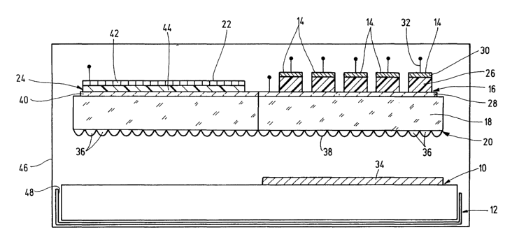
The optical measuring device shown in the diagram serves to photometrically
analyse or evaluate diagnostic test strips 10, for example for glucose tests
in blood
samples. It comprises a positioning unit 12 for the test strips 10 and a
composite
CA 02506790 2005-05-19
-6-
structure consisting of a light source 16 formed by at least one organic light-
emitting diode (OLED 14), a support substrate 18, an imaging optics 20 and a
photodetector 24 having at least one polymer photodiode 22.
In the embodiment shown in fig. 1 several OLEDs 14 arranged in a matrix-like
manner are provided which have different emission wavelengths. The film-like
OLEDs 14 are based on at least one thin organic light-emitting layer 26 which
is
arranged in a sandwich formation between two electrode layers 28, 30. When a
voltage is applied, positive charges are displaced from the anode layer 28
into the
light-emitting layer 26, while electrons are injected onto the cathode layer
30. As a
result of the electrical field, the injected charge Garners each move to the
opposite
electrode layer. If electrons and holes meet, electron-hole pairs are formed
which
can recombine while emitting radiation. The emission spectrum is determined by
the organic semiconductor material that is used. Highly efficient OLEDs
contain
further injection and transport layers to optimize this injection
electroluminescent
effect and auxiliary layers as diffusion barners and for homogenization.
In the embodiment of flg. 1 a common anode 28 adjoining the support substrate
18
is provided which is composed of ITO (indium-tin-oxide) or related oxidic
compounds as well as conducting polymers and is permeable to the emitted
light. In
contrast the cathodes 30 consisting of a metal layer can be individually
controlled by
separate pick-ups 32.
The different wavelengths of the controlled OLEDs enable different optically
detectable reactions or properties of the analytical test areas 34 to be
evaluated on
the test strip 10. In addition the matrix arrangement of the OLEDs enables
different
illumination target areas or illumination spots to be irradiated in order to
for
example examine very small sample volumes on a given test area 34 in a
spatially
resolved manner.
CA 02506790 2005-05-19
The support substrate 18 is composed of a thin flat material that is permeable
to the
generated light and in particular a thin glass or flexible polymer film or a
suitable
multilayer. The OLEDs 14 that are mounted thereon can be manufactured as layer
emitters in extremely small dimensions. For example the pixel size can be
between
50 and 200 ~m whereas the layer thickness of the light-emitting layer 26 can
be in
the range of 100 nm. Such structures can be produced with high precision by a
variety of process techniques such as dipping methods, spin and dip coating,
sieve
and inkjet printing, PVD and CVD methods.
The imaging optics 20 is mounted on the side of the support substrate 18 that
is
opposite to the OLEDs 14. It has a plurality of two-dimensionally distributed
lens
units 36 to couple out the measuring light on the emitter side and couple in
the
measuring light on the detector side. They can be laminated onto the side of
the
substrate facing the test element 10 as a prefabricated microstructured lens
structure
38 for example in the form of a hot-stamped film material. Alternatively the
lens
structure can be directly moulded onto the free substrate side for example by
embossing.
Like the OLEDs the polymer photodiode 22 is a sandwich structure composed of
two electrode layers 40, 42 and a semiconducting polymer layer 44. Such photo-
sensitive layer cells are known and described for example in the publication
of Dey
et al., A dyelpolymer based solid state thin film photoelectrochemical cell
used for
light detection, Synthetic Metals 118 (2001 ), p. 19 - 23 the contents of
which are
hereby incorporated.
Instead of a single photodiode 22, it is also possible for a plurality of
photodiodes to
be arranged on the support substrate 18 as a one-dimensional or two-
dimensional
array or diode field. It is also conceivable that a conventional photometric
receiver
is combined with an OLED light source as described above.
CA 02506790 2005-05-19
_g_
The composite structure comprising OLED 14, imaging optics 20 and photodiode
22 enables a very compact and optically precise photometer arrangement to be
achieved which can be provided to the user in a compact housing 46 in order
that he
himself may evaluate test strips 10 that are in particular designed as
disposable
articles. For this purpose a holder 48 that can be inserted into the housing
46 is
provided as a positioning unit for the test strip 10.
In the arrangement of fig. 1 the optical path extends from the light source 16
through the substrate 18 and the imaging optics 20 onto the test area 34 and
is
reflected or remitted there via the imaging optics 20 through the substrate 18
into
the detector 24. However, a transmissive arrangement is also basically
possible in
which the test strip 10 is examined in the transmitted light between the light
source
and detector.
According to fig. 1 an image of each OLED 14 is formed on a target area on the
test
strip 10 by a group of lens units 36. The embodiments shown in fig. 2 and 3
differ
therefrom essentially in that each OLED 14 has an associated single lens 36
with a
large lens diameter. According to fig. 2 this is designed as a Fresnel lens
36' and its
design is optimized for microstructuring and moulding technology. Fig. 3 shows
an
aspherical collecting lens 36" for focussing the emitted light.
In the embodiment of figs. 2 and 3 special anode layers of the OLEDs 14 are
provided as individually controllable front electrodes while a continuous
cathode
layer 30 forms a common rear electrode.
In the embodiment example shown in fig. 4 a housing 50 is provided for
hermetically screening the free surface of the OLED 14 from the environment in
order to protect the organic light-emitting layer 26 as well as the transport
/ injection
layers 52 and metal electrodes 30 from oxidation by oxygen and from the
effects of
moisture. The edge of the housing 50 can be attached to the electrode layer 28
or the
CA 02506790 2005-05-19
-9-
support substrate 18 by an adhesive layer 54 and the housing can contain a
desiccant
56 as an additional protection against moisture. It is obvious that a layer or
similar
means can be provided together with the support substrate 18 as a material-
tight
barrier instead of a separate housing.
A further embodiment is shown in fig. 5 with a plurality of elementary
photometers
58 arranged on the surface of the support substrate in a matrix-like manner.
Each of
the elementary photometers 58 are formed on a quadratic pixel area by a cross-
shaped polymer photodiode 22 and four OLEDs 14 arranged in the corner areas
that
operate with different wavelengths where of course other local combinations
are
also possible. This allows a target area on the test element 10 to be
optically
scanned in a spatially resolved manner as illustrated in fig. 5 by the circle
60. This
allows small amounts of sample to be photometrically analysed even when the
positioning is inaccurate. At the same time it also enables the optical
measuring path
to be reduced and optionally allows one to even dispense with an imaging
optics.