Note: Descriptions are shown in the official language in which they were submitted.
CA 02507454 2005-05-16
-1-
FERROELECTRIC ELECTRON BEAM SOURCE
AND METHOD FOR GENERATING ELECTRON BEAMS
BACKGROUND OF THE INVENTION
Field of the Invention:
[0001] This invention relates to a ferroelectric electron beam source
and a method for generating electron beams.
Background of the art:
[0002] Such a phenomenon as electron emission from a ferroelectric
substance is known since a long time ago, which phenomenon is
originated from the change of spontaneous polarization such as phase
transition of shielding electrons trapped by the ferroelectric surface.
The emission electron current is weak, but high energy. For example,
when C02 laser was irradiated onto LiNb03, electron emission of
100keV and 10-9A/cm2 was observed.
[0003] With the electron emission system which was established in
CERN (European nuclear cooperative research organization) at 1988,
electron emission with a current density of 7A/cm'' and an intensity of
3KeV at maximum was realized by inverting the spontaneous
polarization of a ferroelectric substance at high speed with a high
speed pulsed voltage. Since then, an attention is paid to such an
electron beam source as utilizing a ferroelectric substance, which is
expected for the practical use as a flat display or a new type process
plasma source. However, if the dielectric constant of the ferro-
electric substance is relatively low and the voltage-resistance of the
ferromagnetic substance is relatively high, the electron beam source
can not generate the electron beams.
Disclosure of the Invention:
Problem to be solved by the Invention:
[0004] It is an object of the present invention to provide a new
ferroelectric electron beam source and a new method for generating
electron beams whereby electron beams with sufficient intensity can
be generated even though the dielectric constant of the ferroelectric
CA 02507454 2005-05-16
-2-
substance to be employed is low and the voltage-resistance of the
ferroelectric substance to be employed is high.
Means for solving the Problem:
[0005] In order to achieve the object, this invention relates to a
ferroelectric electron beam source comprising:
a ferroelectric thin film,
a comb-shaped electrode formed on a main surface of the
ferroelectric thin film, and
a planer electrode formed on a rear surface of the ferroelectric
thin film which is opposite to the main surface of the ferroelectric thin
film,
wherein a property of the main surface of the ferroelectric thin
film is converted in semi-conduction, and a first negative voltage is
applied to the comb-shaped electrode to polarize the ferroelectric thin
film and a second negative voltage is applied to the planer electrode,
thereby generating electron beams from the main surface of the
ferroelectric thin film.
[0006] Also, this invention relates to a method for generating
electron beams, comprising the steps of:
preparing a ferroelectric thin film,
forming a comb-shaped electrode on a main surface of the
ferroelectric thin film,
forming a planer electrode on a rear surface of the ferroelectric
thin film which is opposite to the main surface of the ferroelectric thin
film,
converting a property of the main surface of the ferroelectric thin
film into semi-conduction,
polarizing said ferroelectric thin film by applying a first negative
voltage to the comb-shaped electrode, and
emitting electron beams from the main surface of the ferroelectric
thin film by applying a second negative voltage to the planer electrode.
[0007] According to the present invention, the comb-shaped
electrode and the planer electrode are provided on the main surface
CA 02507454 2005-05-16
-3-
and the rear surface of the ferroelectric thin film, respectively, which
are opposite to one another, and the property of the main surface on
which the comb-shaped electrode is converted into semi-conduction.
Then, the assembly comprised of the ferroelectric thin film, the comb-
s shaped electrode and the planer electrode is disposed in vacuum
atmosphere, and the ferroelectric thin film is polarized by applying a
negative voltage to the comb-shaped electrode. In this case, positive
polarized charge is induced on the main surface of the ferroelectric
thin film, and negative polarized charge is induced on the rear surface
of the ferroelectric thin film. Since the property of the main surface
is converted in semi-conduction, the positive polarized charge is
neutralized by the electrons from the comb-shaped electrode via the
main surface.
[0008] Under the circumstance, when the polarization of the
ferroelectric thin film is inverted by applying a negative voltage to the
planer electrode, negative polarized charge is induced on the main
surface. In this case, the electrons neutralizing the positive polarized
charge induced on the main surface are sputtered through the coulomb
repulsive force against the negative polarized charge, thereby
generating electron beams.
[0009] In the case that the property of the main surface of the
ferroelectric thin film is not converted into semi-conduction, if the
ferroelectric thin film is made of a material of low dielectric constant
and high voltage resistance such as polyvinilidene-fluoride (PVDF),
the electrons to neutralize the positive polarized charge are not
supplied on the main surface. Therefore, even though the negative
voltage is applied from the planer electrode, the intended electrons can
not be generated.
[0010] In the case that the property of the main surface of the
ferroelectric thin film is not converted into semi-conduction, discharge
may be generated at the comb-shaped electrode through the polarization
inversion, thereby deteriorating the main surface. In contrast, in the
case that the property of the main surface of the ferroelectric thin film
CA 02507454 2005-05-16
-4-
is converted into semi-conduction, the discharge can be prevented,
thereby not deteriorating the main surface and realizing the electron
emission. In the case that the property of the main surface of the
ferroelectric thin film is converted into insulation, the electron
emission can not be realized through the polarization inversion
because the electrons neutralizing the polarized charge are not
generated.
[0011] In this way, according to the present invention, the intended
electron beams can be generated irrespective of the magnitudes of the
dielectric constant and the voltage resistance of a material making the
ferroelectric thin film.
[0012] The present invention can be applied to a ferroelectric thin
film with high dielectric constant and low voltage resistance in
addition to the ferroelectric thin film with low dielectric constant and
high voltage resistance as mentioned above. However, when the
ferroelectric thin film is made of such a material with low dielectric
constant and high voltage resistance as an organic ferroelectric
material of PVDF, vinylidenefloride-trifluoroetylene copolymer, etc.,
or an inorganic ferroelectric material of lead zirconate titanate, barium
titanate, etc., the intended electron beams can be generated and emit
sufficiently.
[0013] In the present invention, the electron emission can be
performed for a gaseous substance, a liquid substance or a solid
substance which is disposed on the main surface of the ferroelectric
thin film on which the comb-shaped electrode is provided, in addition
to in vacuum. For example, when an insulative solid is disposed on
the main surface of the ferroelectric thin film on which the comb-
shaped electrode is disposed, the electron beams can be injected into
the insulative solid. Therefore, if a given dye is incorporated in the
insulative solid, the dye is excited by the electron beams, thereby
generating a light with a given wavelength from the insulative solid.
[0014] The conversion of the main surface of the ferroelectric thin
film into semi-conduction can be realized by forming a given semi-
CA 02507454 2005-05-16
-5-
conductive thin film on the main surface or performing conducting
treatment such as etching treatment using etchant or plasma treatment.
[0015] Herein, the term "semi-conduction" means an intermediate
electric property between metallic conductor and insulator which can
not flow current.
[0016] According to the present invention can be provide a new
ferroelectric electron beam source and a new method for generating
electron beams whereby electron beams with sufficient intensity can
be generated even though the dielectric constant of the ferroelectric
substance to be employed is low and the voltage-resistance of the
ferroelectric substance to be employed is high.
Brief Explanation of the Drawings:
[0017] For better understanding of the present invention, reference
is made to the attached drawings, wherein
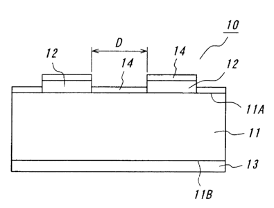
Fig. 1 is a cross sectional view illustrating a ferroelectric
electron beam source according to the present invention, and
Fig. 2 is a top plan view of the ferroelectric electron beam
source illustrated in Fig. 1.
Preferred Embodiments for Carr~g Out the Invention:
[0018] Details, other features and advantages of the present
invention will be described hereinafter, with reference to "Preferred
Embodiments far Carrying out the Invention".
[0019] Fig. 1 is a cross sectional view illustrating a ferroelectric
electron beam source according to the present invention, and Fig. 2 is
a top plan view of the ferroelectric electron beam source illustrated in
Fig. 1. The ferroelectric electron beam source 10 illustrated in
Figs. 1 and 2 includes a ferroelectric thin film 11, a comb-shaped
electrode 12 formed on the main surface 11A of the ferroelectric thin
film 11 and a planer electrode 13 formed on the rear surface 11B of the
thin film 11. As is apparent from Fig. 2, the comb-shaped electrode
12 is elongated in strip on the main surface 11A of the ferroelectric
thin film 11. The planer electrode 13 is formed so as to cover the
rear surface 11B of the ferroelectric thin film 11.
CA 02507454 2005-05-16
-6-
[0020] As is not apparent from the drawings, the rims of the comb-
shaped electrode 12 and the planer electrode 13 are removed through
etching so as to prevent the discharge between the electrodes.
[0021] In the ferroelectric electron beam source 10 illustrated in
Figs. 1 and 2, the ferroelectric thin film 11 may be made of any
material exhibiting ferroelectric properties, but preferably made of a
material with low dielectric constant and high voltage resistance such
as an organic ferroelectric material of PVDF, vinylidenefloride-
trifluoroetylene copolymer, etc., or an inorganic ferroelectric material
of lead zirconate titanate, barium titanate, etc. In this case, the
thickness of the ferroelectric thin film 11 is preferably set within
1-2000 p,m. If the thickness of the ferroelectric thin film 11 is set
beyond 1000 hum, the absolute value of the impulse voltage to be
applied to the ferroelectric thin film 11 becomes large in the order of
several thousands voltages, for example, in the electron beam
generating method which will be described below, thereby deteriorating
the operationality of the ferroelectric electron beam source 10.
On the other hand, if the thickness of the ferroelectric thin film 11 is
set below 1 p.m, the ferroelectric electron beam source may have
difficulty in the use for a light-emitting device.
[0022] The comb-shaped electrode 12 and the planer electrode 13
may be made of a normal material such as Au, Ag, Cu, Al.
The distance (pitch) D between the rods of the comb-shaped electrode
12 is preferably set to the thickness of the ferroelectric thin film 11 if
the ferroelectric thin film 11 is made of the above-mentioned
preferable material with low dielectric constant and high voltage
resistance and the thickness of the ferroelectric thin film 11 is set to
the above-mentioned preferable range.
[0023] The semi-conductive film 14 may be made of any kind of
material only if the intended electron beams can be emit through the
polarization-inverting operation, but preferably made of C-Au-S, C-
Cu-S, C-Fe-S or the like. The thickness of the semi-conductive film
14 is set within 0.5-lOnm.
CA 02507454 2005-05-16
_7_
[0024] Then, the generating method of electron beams utilizing the
ferroelectric electron beam source 10 illustrated in Figs. 1 and 2 will
be described. First of all, the assembly comprised of the ferroelectric
thin film 11, the comb-shaped electrode 12 and the planer electrode 13
is disposed in a given atmosphere. Then, a given negative voltage is
applied to the comb-shaped electrode 12 to polarize the ferroelectric
thin film 11. In this case, positive polarized charge is induced on the
main surface 11A of the ferroelectric thin film 11. On the other hand,
the positive polarized charge is neutralized by the electrons from the
comb-shaped electrode 12 via the semi-conductive film 14.
[0025] Under the circumstance, a negative impulse voltage is
applied to the planer electrode 13 to invert the polarization of the
ferroelectric thin film 11. In this case, since negative polarized
charge is induced on the main surface 11, the electrons neutralizing the
positive polarized charge induced on the main surface 11A are
sputtered through the coulomb repulsive force against the negative
polarized charge, thereby generating the intended electron beams.
[0026] The intended electron beams can be generated by applying an
AC voltage with appropriately controlled frequency to the comb-
shaped electrode 12 and the planer electrode 13, instead of the
application of the negative impulse voltage.
[0027] In the case that the semi-conductive film 14 is not formed on
the main surface 11A of the ferroelectric thin film 11, if the ferro-
electric thin film 11 is made of a material with low dielectric constant
and high voltage resistance such as PVDF, the electrons to neutralize
the positive polarized charge are not supplied onto the main surface
11A even though the positive polarized charge is induced on the main
surface 11A as mentioned above. Therefore, when the negative
impulse voltage is applied from the planer electrode 13, the intended
electron beams can not be generated.
[0028] If a given insulative solid is disposed on the main surface
11A of the ferroelectric thin film 11 via the semi-conductive thin film
14, the electron beams can be injected into the insulative solid.
CA 02507454 2005-05-16
_$_
In this point of view, if a given dye is incorporated into the insulative
solid, a light originated from the dye can be generated through the
excitation of the dye. If a thin film with a given energy band structure
is formed on the main surface 11A, a light originated from the
recombination of electrons and holes can be generated.
[0029] If another solid substance, gaseous substance or liquid
substance is disposed on the main surface 11A, instead of the above-
mentioned insulative solid, the electron beams can be injected into the
substance.
Example:
[0030] A PVDF sheet with a thickness of 40 wm was prepared, and
an Al comb-shaped electrode with a rod distance (pitch) of 50 p.m was
formed on the main surface of the sheet, and an Al planer electrode
was formed on the rear surface of the sheet. Then, the assembly
comprised of the sheet and the electrodes was disposed in a vacuum
atmosphere under a pressure of 10-4 Torr or below. When a negative
voltage of -450V was applied to the comb-shaped electrode and a
negative impulse voltage of -2400V was applied to the planer electrode,
electron beams with a charge of 6.1 x 10⁻¹²C can be generated.
[0031] Although the present invention was described in detail with
reference to the above examples, this invention is not limited to the
above disclosure and every kind of variation and modification may be
made without departing from the scope of the present invention.
[0032] For example, in the above embodiment, although the semi-
conductive film 14 is formed on the main surface 11A of the
ferroelectric thin film 11 such that the property of the main surface
11A is converted into semi-conduction, the property of the main
surface 11A can be also converted into semi-conduction through
conducting treatment such as plasma treatment or etching treatment
using etchant for the main surface 11A. The etching treatment can be
carried out by using Na treatment (treatment using an etchant with
metallic Na immersed in an oil). The plasma treatment can be carried
out by using Ar, NZ or O? plasma.