Note: Descriptions are shown in the official language in which they were submitted.
CA 02507663 2005-05-27
WO 2004/050287 1 PCT/EP2003/013519
Method for soldering miniaturized components
to a baseplate
The present invention relates to a method for highly
precise fixing of miniaturized components to a
baseplate by means of a solder joint. In particular,
the invention relates both to a laser soldering method
for fixing microoptical components to a baseplate which
is at least partly transparent to laser beams and is
coated with a metallic layer and to the baseplate
obtained by this method and a substrate for use in the
method.
Different methods for fixing miniaturized components by
means of a solder joint are known from the prior art.
WO 99/26754 describes a method for soldering
miniaturized components to a baseplate. The baseplate
is at least partly coated with a lattice-like metal
pattern or metal structure. According to WO 99/26754,
the patterned structure can be formed by a lattice of
planar elements or a number of stripes which preferably
intersect one another perpendicularly and form a
lattice or some other structure which is characterized
by a uniform alternation of metal regions and free
regions. The planar elements may assume a rectangular
shape, a square shape, a round shape or any shape which
is suitable for use in this method. Here, the pattern
step width should be at least one order of magnitude
smaller than the dimensions of the component side to be
fixed. The solder material is preferably applied to the
component side to be fixed or optionally to the metal
CA 02507663 2005-05-27
WO 2004/050287 ' 2, PCT/EP2003/013519
pattern of the baseplate. The component is arranged
above the baseplate, the metal pattern and the solder
material layer of the component or the solder material
layer on the metal pattern and the component side being
located opposite one another without contact and a
vertical distance apart. Heat energy is then supplied
from the uncoated side of the baseplate for melting the
solder material or the solder material layer on the
coated side on which the component is also arranged
until drop formation of the solder material occurs,
with the result that the solder material drops fill the
intermediate space between the component and the
baseplate for mutual fixing. The metallized sample
regions provide a fixing region for the solder
material, while the metal-free regions make it possible
for a sufficient quantity of energy to pass through the
baseplate in order to melt the solder material. When
heat energy is supplied, a part of the energy thus
passes through the uncoated regions of the metal
pattern. The part which reaches those regions of the
metal pattern which are coated with the metal either
heats up the metal layer or is reflected. The energy is
preferably applied by means of a laser beam. Owing to
the lattice structure of the metal pattern on the
baseplate, the choice of a suitable light absorption
coefficient of the metal layer is particularly
problematic since, on the one hand, the baseplate is
not permitted to overheat and, on the other hand, a
certain minimum temperature is required for carrying
out the process. Usually, metal of the metal pattern
covers about 70% of the surface of the baseplate. Less
than 30% of the power of the laser beam is used for
heating the solder material since one part of the
CA 02507663 2005-05-27
WO 2004/050287 3 PCT/EP2003/013519
approximately 700 of the remaining power heats up the
baseplate and the other part is reflected.
For carrying out the soldering process, more than 15 W
are required for the duration of 2 seconds. Different
types of metal coatings are required depending on the
chosen material of the baseplate. Moreover, a discrete
effect occurs owing to the metal pattern if the solder
material wets only those regions of the metal pattern
which are coated with the metal layer but - in
particular owing to the flow behaviour and the surface
tension - not the uncoated metal-free regions of the
metal pattern. Particularly in the case of a metal
pattern which is coarse in relation to the side of the
component side to be fixed, the result may therefore be
asymmetric off centre soldered seams which - owing to
the shrinkage of the solder material which inevitably
takes place during solidification - are associated with
a change in position of the component and/or a skew
position.
In practice, it has been found that the solder material
cools substantially more rapidly close to the
transverse sides of the component than the remainder of
the solder material. This can lead to asymmetries of
the solidified solder material.
Since the fixing is effected by soldering of two
different materials, different coefficients of thermal
expansion in the case of the solder material and of the
baseplate cause high stresses and distortions after the
soldering process has been carried out. Depending on
the mechanical resistance of the carrier material,
CA 02507663 2005-05-27
WO 2004/050287 4 PCT/EP2003/013519
parasitic local deformation may occur in the region of
the solder joint owing to the high stresses.
By means of the known method described above, it is
possible to achieve accuracies of about 2 microns in
the 6 degrees of freedom. Particularly in the mounting
of components which contain or carry microoptical
elements, however, even higher accuracies of mounting
are required.
There is therefore the need to improve the method
described above and disclosed in WO 99/26754 in order
to achieve a higher accuracy of mounting of
miniaturized components, in particular microoptical
elements, on a carrier plate and to optimize the entire
method from the economic point of view.
Furthermore, flux-free and/or lead-free soldering is
scarcely possible in the method described above.
Experiments have shown that the use of flux-free solder
material comprising Sn96Ag4 and a metal layer coated
with tin, nickel and gold does not lead to the desired
satisfactory results if the fixing is effected on a
metal pattern as described in WO 99/26754 since a metal
pattern has insufficient wettability.
Numerous further methods for fixing small components on
a carrier plate are known from the area of the
equipping technology for electronic surface-mounted
circuits, SMD technology. In the case of electronic
circuits, however, the requirements are completely
different from those in the area relating to the
mounting of microoptical components since lower
CA 02507663 2005-05-27
WO 2004/050287 5~ PCT/EP2003/013519
precisions are required in the case of electronic
circuits and highly accurate orientation in all 6
degrees of freedom is not required. Moreover,
electronic circuits must by definition be composed of
interrupted metal layers since it would be inexpedient
to mount a large number of electronic components on a
circuit board having a single uninterrupted metal
layer. The completely free positionability of
components on a carrier plate is neither required nor
desired in the case of electronic circuits but is of
decisive importance, for example, for building up a
microoptical system on a carrier plate. Thus,
approaches from electronic circuit board equipping
technology are suitable only to a limited extent.
It is an object of the present invention to provide a
method for fixing a miniaturized component, in
particular comprising at least one microoptical
element, to a baseplate by means of a solder joint,
which method is distinguished by increased positional
accuracy of the components compared with the known
method and high cost-efficiency.
This object is achieved by realizing the features of
the independent Claims. Features which develop the
invention in an alternative or advantageous manner are
evident from the dependent Patent Claims.
According to the invention, in order to fix a
miniaturized component, comprising in particular a
microoptical element, with its base surface to a
baseplate by means of a solder j oint, the baseplate is
coated with a metal layer, the metal layer being
CA 02507663 2005-05-27
WO 2004/050287 6I PCT/EP2003/013519
applied in a continuously planar manner and hence being
free of interruptions. The baseplate and the metal
layer form a so-called substrate. The solder material
is applied to the metal layer of the baseplate.
Thereafter, the component is arranged above the
baseplate, the solder material and the base surface of
the component being present opposite one another
without contact, a vertical distance apart and so as to
form an intermediate space. By supplying heat energy in
a region of the bottom of the baseplate, which region
is locally limited substantially to the fixing section,
the solder material is melted so that the intermediate
space between the metal layer and the base surface of
the component is filled by drop formation of the molten
solder material for mutual fixing - optionally assisted
by lowering of the component. As a result of
solidification of the solder material, the mutual
fixing is implemented.
Owing to the continuous, extensive metal layer, a
substantially higher final accuracy of positioning of
the component on the baseplate is achieved in
comparison with the method of WO 99/26754 which employs
the metal pattern, since the continuous metal surface
is wet easily and more homogeneously with the solder
material than is the case with an interrupted metal
structure.
Moreover, the higher absorption coefficient of the
metal layer results in a reduction of 40% in the laser
beam power required for soldering, compared with the
method of WO 99/26754. Thus, a laser power of less than
10 W for 2 seconds is sufficient for carrying out the
CA 02507663 2005-05-27
WO 2004/050287 7, PCT/EP2003/013519
soldering. By reducing the required power, the danger
of damage to the components to be fixed also decreases
considerably, especially if they are microoptical
components which are very heat-sensitive. The laser
beam is substantially better absorbed by the metal
layer than in the known method. It is therefore
possible to use alloys having a high melting point. For
the method according to the invention, the absorption
coefficient of the metal layer need only be maximized
to permit soldering on different types of baseplates,
whereas the soldering power of the laser need only be
adapted to the thermal expansion of the baseplate.
Since, in the method of the present invention, an
uninterrupted, continuously planar metal layer is used,
a considerable cost reduction in the production of the
substrate is possible since a continuous metal layer
can be substantially more easily produced than a metal
pattern.
Of course, it is not necessary for the continuously
planar metal layer to be applied to the entire
baseplate. It is of course possible to apply to the
baseplate a plurality of cohesive metal layers which
are not connected to one another. In that fixing
section in which the component is to be fixed with its
base surface to the baseplate, however, the metal layer
is substantially free of interruptions and continuously
planar. It is possible to apply a plurality of planar
elements to a baseplate in a pattern, which elements
are each cohesive and continuously planar, but each
planar element represents a separate fixing section to
which the component is to be fixed, so that the
CA 02507663 2005-05-27
WO 2004/050287 ~ 8~ PCT/EP2003/013519
projection of the base surface of the component is
completely covered by one planar element. Continuously
planar also does not inevitably mean a metal layer
having an absolutely uniform layer thickness but a
substantially cohesive surface which has substantially
no interruptions, apart from small interruptions which
occur in particular in the case of small layer
thicknesses but are not produced artificially in the
form of a patterned structure.
In an embodiment of the invention, the solder material
is placed on the metal layer in the form of a flat
piece which has, for example, the shape of a truncated
cylinder. Thereafter, the component is arranged with
its base surface above the solder material. An energy
source, for example laser, is aligned below the
baseplate and emits an energy beam from the bottom of
the baseplate. The energy beam passes through the
baseplate and strikes the metal layer on the top of the
baseplate. The metal layer is subjected to localized
heating here and thus heats the solder material, in a
manner comparable with a stove plate. The flat piece of
solder material melts and, in the liquefied state,
assumes a drop-like form owing to the surface tension
of the solder. Moreover, the solder material expands by
a few hundred microns owing to the heating. As a result
of the drop form and the expansion, the distance
between the solder material and the base surface of the
component decreases. Wetting of the base surface of the
component with solder material thus occurs, so that a
solder joint can be produced.
Alternatively, it is possible to reduce the
CA 02507663 2005-05-27
WO 2004/050287 ~ 91 PCT/EP2003/013519
intermediate space between the metal layer and the base
surface of the component by lowering the component from
a starting position towards the baseplate so that the
base surface of the component dips into the molten
solder material and the base surface of the component
is thus wet with the solder material. Optionally, the
component is withdrawn again to the starting position
thereafter - before the beginning of solidification. In
this embodiment, but also in the first one, it is
conceivable to apply the solder material also or
exclusively to the base surface of the component.
Since, however, heating of a solder material which is
bonded to the metal layer directly heated by the
radiation is more effective, better results are
obtained with a solder material applied directly to the
metal layer.
In a further embodiment of the invention, the solder
material is applied at least to a part of the metal
layer of the baseplate, discretely in the form of a
multiplicity of solder material elements a distance
apart, for example in the form of a spot pattern, or in
a continuously planar manner in the form of an
uninterrupted layer. Here, this part is substantially
larger than the actual fixing section which an
individual component occupies. Optionally, the entire
metal layer is coated with the solder material. An
energy source, for example a laser, is aligned, as in
the above method, below the baseplate and emits an
energy beam from the bottom of the baseplate. The
energy beam passes through the baseplate and strikes
the metal layer. The latter heats up in a narrowly
localized region and melts the solder material layer or
CA 02507663 2005-05-27
~ 1
WO 2004/050287 10 PCT/EP2003/013519
the solder material pattern within this region. Drop
formation occurs in this region owing to the surface
tension of the solder. Thus, optionally by additional
lowering of the component, the base surface of the
component is wet with solder material so that a solder
joint can be produced.
In another embodiment of the invention, a solder
material in the form of a flat piece, in particular a
truncated cylinder, is arranged on the baseplate, the
cross-section of the flat piece being smaller than the
cross-section of the base surface of the component, so
that the projection of the base surface of the
component onto the metal layer of the baseplate
completely covers the cross-section of the flat piece -
prior to melting. By reducing the cross-section of the
flat piece, even higher accuracy of fixing is
achievable.
By means of the soldering method according to the
invention, accuracies of fixing in the region of
0.25 micron are achieved, so that this method is
outstandingly suitable for the highly precise mounting
of microoptical components on a baseplate.
The method is described in detail below. The invention
is illustrated below by a specific embodiment with
reference to figures.
The base surface of the miniaturized component must
have good wettability for solder material. This base
surface may be flat or convex, for example in the form
of a convex spherical surface section or of a convex
CA 02507663 2005-05-27
WO 2004/050287 ~ 11~ PCT/EP2003/013519
cylinder lateral surface section. A spherical base
surface simplifies exact alignment of the component
owing to the symmetry. By means of a rotationally
symmetrical solder joint between the baseplate and the
component, a stable joint having little distortion in
the case of shrinkage and having good repeatability is
achieved. This increases the process reliability and is
particularly important for mass production.
Since the energy supply is from that side of the
baseplate which is opposite the side coated with the
metal layer, and hence the energy for heating the metal
layer is supplied through the baseplate, it is
necessary to choose a baseplate which is substantially
transparent for the wavelength of the energy provided.
If a laser beam is used as the energy source, the
baseplate should have high transparency for the laser
beam wavelength.
Moreover, the coefficients of thermal expansion of the
baseplate and of the metal layer must correspond to the
extent that no tearing or buckling of the metal layer
should occur during or after the supply of the energy.
Ideally, the coefficient of thermal expansion of the
baseplate is equal to that of the metal layer. The
material used for the production of the baseplate
should be capable of withstanding high thermal loads
since, on supplying energy, for example by means of a
laser or UV, a part of the energy passed through the
baseplate is inevitably absorbed by the baseplate.
Moreover, strong heating occurs in a region of the
metal layer which has high conductivity, and it is for
this reason that the baseplate too is strongly heated
CA 02507663 2005-05-27
.
WO 2004/050287 12 PCT/EP2003/013519
in a locally limited region. If the baseplate comprises
a material having poor thermal conductivity, for
example glass, ceramic or glass ceramic, there is a
high energy concentration in the locally limited
region. This could lead to failure of the material in
the case of an unsuitable choice of material. If the
mutual alignment of a plurality of components is
important, it is also necessary to ensure that no
material which has a high coefficient of thermal
expansion is chosen as the baseplate since the
alignment of the optical components changes in the
event of heating of the baseplate. This would
inevitably lead to optical errors in the optical
system. Suitable materials for the baseplate are, for
example, glass, sapphire, ceramic, glass ceramic,
silicon or Pyrex. Further suitable materials are known
from the prior art.
The metal layer may be formed from a plurality of
layers of different metals and alloys and optionally
coated with an antioxidant, flux, etc. Preferably, the
alloy of the metal layer should have little tendency to
oxidize and should contain gold.
In an embodiment of the invention, a sapphire piece or
a Pyrex wafer having a thickness of about 1 to
2 millimetres is chosen as the baseplate. The wafer is
coated with a metal layer comprising chromium, nickel
and gold. The metal layer has a thickness of about
1 micron. The solder material chosen is, however, SnPb
or Sn96Ag4, which fills a gap between the metal layer
and the base surface of the component of 0.2 to
0.5 millimetre.
CA 02507663 2005-05-27
WO 2004/050287 13~ PCT/EP2003/013519
The shrinkage of the solder material during cooling
inevitably ensures a vertical offset of the component
perpendicularly to the baseplate. It has good
repeatability and is a function of the gap between the
baseplate and the base surface of the component. For
compensation of this vertical shrinkage, it is possible
to position the component correspondingly higher and to
take the shrinkage into account in the prepositioning.
In a further embodiment of the invention, the accuracy
of mounting is further increased, especially in the
case of an inclined component, by reducing the cross-
section of the solder material, for example the
diameter of the flat piece, so that this cross-section
is smaller than that of the base surface of the
component. In this case, the diameter d of the flat
piece of solder material is smaller than the diameter D
of the base surface of the component. At the latest
after solidification of the solder material, the
diameter of the solidified solder material is smaller
than the diameter D of the base surface. This results
in less asymmetries on solidification of the solder
material, which may occur in particular because of the
fact that the solder material cools substantially more
rapidly on the transverse surfaces than in the middle.
Especially in the case of inclined mounting of a
component, it is therefore advantageous to provide a
solder joint with little solder material since, in this
case, shrinkages do not have an effect to such an
extent. Moreover, there are in this case fewer stresses
which result from the cooling and the associated
shrinkage, so that the manufacturing accuracy is
further increased.
CA 02507663 2005-05-27
WO 2004/050287 ~ 14~ PCT/EP2003/013519
The method is suitable in particular for use in an
automatic, flux-free laser soldering process since
substantially all required steps can be carried out by
handling robots which have a highly accurate position
sensor system. Thus, each component can be positioned
in a highly precise manner freely in space in all 6
degrees of freedom. The free positionability, which is
not inevitably limited by predetermined regions on the
baseplate, is a further advantage of the invention. If
the entire baseplate is coated with the metal layer, it
is possible to position the component in any desired
position on the baseplate either by free positioning of
a flat piece of solder material or by means of a solder
material layer.
This technique described here is suitable in particular
for highly accurate fixing of microoptical components,
oriented in all 6 degrees of freedom. Thus, the
miniaturized component may serve as a holder for a
microoptical element, for example a lens, an optical
fibre, a laser diode, etc. Such microoptical components
typically have a diameter of the order of magnitude of
2.6 mm and a height of 3.5 mm. A possible example of a
holding device for a microoptical component is
described in EP 1127287 Bl.
A further embodiment of the invention comprises a
baseplate having a plurality of miniaturized components
which are arranged within a component region of the
baseplate and in each case have at least one
microoptical element. At least the component region of
the baseplate is coated on the top with at least one
metal layer, the metal layer on the top of the
CA 02507663 2005-05-27
WO 2004/050287 I 15~ PCT/EP2003/013519
baseplate being applied in a continuously planar manner
at least in the component region and hence being free
of interruptions. The components are fixed with the
base surface above in each case one solder joint on the
metal layer. The baseplate is transparent to laser
radiation. The component region is a part of the
baseplate on which a plurality of parts are arranged on
the cohesive metal layer. In a possible embodiment, the
metal layer is applied in a continuously planar manner
to the entire top of the baseplate and hence
substantially without interruptions. In this case, the
component region is formed by the entire baseplate. The
solder material of the solder joint preferably has a
concave outer surface.
In a special embodiment, at least one of the plurality
of components comprises a holder for holding a
supporting part on which the at least one microoptical
element in each case is fixed, the holder being
connected to the supporting part, and the supporting
part to the microoptical element, by means of soldering
points. Such a holder is also described in
EP 1127287 B1.
The substrate for use in the method according to the
invention is formed by a baseplate which is transparent
to laser radiation and is coated on one side with at
least one metal layer which is applied in a
continuously planar manner substantially to the entire
side and is thus substantially free of interruptions.
Optionally, the substrate is coated with a layer of
solder material which is applied in a continuously
planar manner at least to a part of the metal layer of
CA 02507663 2005-05-27
WO 2004/050287 16~ PCT/EP2003/013519
the baseplate, so that the layer of solder material is
free of interruptions in the part. Alternatively, the
layer of solder material is applied, in at least one
part on the metal layer of the baseplate, in a pattern
comprising a multiplicity of solder material elements a
distance apart.
The invention is described in more detail below with
reference to specific embodiments shown schematically
in the drawings. Specifically:
Fig. la, lb show the arrangement of a component, of a
solder material in the form of a small piece
and of a substrate before (Fig. la) and after
(Fig. lb) the production of the solder joint;
Fig. 2a, 2b show the arrangement of a component, of a
solder material in the form of a large flat
piece and of a substrate before (Fig. 2a) and
after (Fig. 2b) the production of the solder
joint;
Fig. 3 shows the determination of the diameter d of a
solder material in the form of a flat piece in
the case of component inclination of amaX = ~5°;
Fig. 4a, 4b show a component and a substrate with a
layer of solder material which is applied in a
pattern comprising a multiplicity of solder
material elements a distance apart, before
(Fig. 4a) and after (Fig. 4b) the production of
the solder joint;
CA 02507663 2005-05-27
WO 2004/050287 17 PCT/EP2003/013519
Fig. 5a, 5b show a component and a substrate with a
layer of solder material applied in a
continuously planar manner, before (Fig. 5a)
and after (Fig. 5b) the production of the
solder joint; and
Fig. 6 shows a component which comprises a holder for
holding a supporting part on which a
microoptical element is fixed.
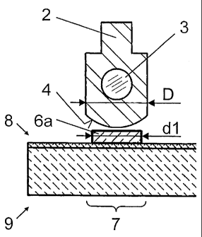
Fig. la and Fig. 2a each show a baseplate 1 having a
top 8 and a bottom 9 in a state before production of a
solder joint. The baseplate 1 which is transparent to
laser radiation is coated on its top 8 with a metal
layer 5 which is applied in a continuously planar
manner so that it is substantially free of
interruptions. The baseplate 1 and the metal layer 5
form a so-called substrate. Within a fixing section 7
on the metal layer 5 a solder material 6a, 6b in the
form of a flat piece, which, in the not yet molten
state, has the shape of a truncated cylinder but may
also have another shape is applied to the metal layer
5. The fixing section 7 is that section on which a
single component 2 is to be fixed or is fixed. A
miniaturized component 2 which carries a microoptical
element 3 is arranged above the fixing section 7 of the
baseplate 1 so that the solder material 6a, 6b and a
convex base surface 4 of the component 2 are present
opposite one another without contact, a vertical
distance apart and so as to form a vertical
intermediate space. The component 2 is positioned and
held in a highly precise manner by means of a robot
station (not shown), the expected vertical shrinkage
CA 02507663 2005-05-27
WO 2004/050287 18~ PCT/EP2003/013519
being taken into account. In Fig. la, the solder
material 6a in the form of a flat piece has a diameter
dl which is smaller than the diameter D of the base
surface 4 of the component 2, so that dl<D, whereas the
solder material 6b in the nonmolten state in Fig. 2a
has a diameter d2 which is equal to the diameter D, so
that d2=D.
By supplying laser radiation locally limited to the
fixing section 7 and passing through the baseplate l,
in the form of a laser beam 11, from the bottom 9 of
the baseplate l, the metal layer 5 is strongly heated
at least within the fixing section 7 and acts as a sort
of stove plate, so that the solder material 6a, 6b
melts, forms a drop owing to the surface tension, wets
the base surface 4, flows into the intermediate space
and thus produces a joint between the metal layer 5 and
the base surface 4. Thereafter, the laser radiation 11
is deactivated again and time is allowed for the molten
solder material 6a', 6b' to solidify. Figures lb and 2b
show the state after production of the joint with the
molten solder material 6a', 6b'. In both cases, the
vertical distance between the component 2 and the
baseplate 1 decreases as a result of the shrinkage of
the solder material 6a', 6b'. Moreover, the diameter of
the molten solder material 6a', 6b' decreases in
comparison with the diameter dl, d2 of the solder
material 6a, 6b in the nonmolten state, it being true
both in Fig. la for dl<D and in Fig. 2a for d2=D that
the diameter of the molten solder material 6a' , 6b' is
smaller than D. Here, the molten material 6a' in
Fig. lb has a smaller diameter than the molten solder
material 6b' in Fig. 2b. The lateral surface of the
CA 02507663 2005-05-27
WO 2004/050287 19~ PCT/EP2003/013519
solder material 6a', 6b' has a concave shape.
Fig. 3 shows the determination of the diameter d of a
solder material 6a in the form of a small flat piece in
the case of an inclination of the component 2 of
amaX = ~5°. Assuming that the diameter D of the base
surface 4 of the component 2 is, for example,
D = 2.6 mm, the radius of the round part of the base
surface 4 is r = 1.6 mm and the angle of inclination of
the component 2 1S Amax = ~5°. a maximum diameter of
dmaX = 2.43 mm is obtained for the diameter d of the
contacting solder material 6a in the form of a flat
piece. The ideal distance arises from the requirement
that the solder material 6a should not be in contact
with the base surface 4 before production of the joint,
even in the case of an inclined component 2. In order
to meet this requirement, the diameter d of the small
flat piece of solder material 6a is reduced by 200
relative to dmax, so that d = 2.43
(1 - 0.2)
- 1. 94 mm.
Fig. 4a and 4b show a component 2 and a substrate
comprising baseplate 1 and metal layer 5 with a layer
of solder material 6c applied in a pattern comprising a
multiplicity of solder material elements 6c " a
distance apart, before (Fig. 4a) and after (Fig. 4b)
the production of the solder joint. The solder material
here 6c in the form of a pattern is applied to the
entire metal layer 5. A locally limited laser beam 11
melts a plurality of solder material elements 6c " of
the solder material layer 6c and causes them to
coalesce to form a drop of solder material 6c' which,
as in Fig. la/lb and 2a/2b, produces the joint between
the base surface 4 of the component 2 and the metal
CA 02507663 2005-05-27
WO 2004/050287 20~ PCT/EP2003/013519
layer 5 of the baseplate 1. Fig. 5a and 5b, on the
other hand, show a component 2 and a substrate having a
layer of solder material 6d applied in a continuously
planar manner, before (Fig. 5a) and after (Fig. 5b) the
production of the solder joint. Here, a laser beam 11
melts a part of the solder material 6d, which forms
into a drop of solder material 6d' and produces a joint
between the component 2 and the baseplate 1.
Fig. 6 shows an embodiment of a component 2 which
comprises a holder 2' for holding a supporting part 2 "
on which a microoptical element 3 is fixed, the holder
2' being joined to the supporting part 2 ", and the
supporting part 2 " to the microoptical element 3 by
means of soldering points 10. In order to permit a
solder joint 10, the component 2 has a base surface 4.