Note: Descriptions are shown in the official language in which they were submitted.
CA 02508362 2005-06-O1
WO 2004/051791 PCT/US2003/037174
MULTI-LAYER CAPACITIVE COUPLING IN PHASED ARRAY ANTENNAS
BACKGROUND OF THE INVENTION
Statement of the Technical Field
The inventive arrangements relate generally to the
field of communications, and more particularly to phased array
antennas.
Description of the Related Art
Existing microwave antennas include a wide variety
of configurations for various applications, such as satellite
reception, remote broadcasting, or military communication. The
desirable characteristics of low cost, light-weight, low
profile and mass producibility are provided in general by
printed circuit antennas. The simplest forms of printed
circuit antennas are microstrip antennas wherein flat
conductive elements are spaced from a single essentially
continuous ground element by a dielectric sheet of uniform
thickness. An example of a microstrip antenna is disclosed in
U.S. Pat. No. 3,995,277 to Qlyphant.
The antennas are designed in an array and may be
used for communication systems such as identification of
friend/foe (IFF) systems, personal communication service (PCS)
systems, satellite communication systems, and aerospace
systems, which require such characteristics as low cost, light
weight, low profile, and a low sidelobe.
The bandwidth and directivity capabilities of such
antennas, however, can be limiting for certain applications.
While the use of electromagnetically coupled microstrip patch
pairs can increase bandwidth, obtaining this benefit presents
significant design challenges, particularly where maintenance
of a low profile and broad beam width is desirable. Also, the
use of an array of microstrip patches can improve directivity
by providing a predetermined scan angle. However, utilizing an
CA 02508362 2005-06-O1
WO 2004/051791 PCT/US2003/037174
array of microstrip patches presents a dilemma. The scan angle
can be increased if the array elements are spaced closer
together, but closer spacing can increase undesirable coupling
between antenna elements thereby degrading performance.
Furthermore, while a microstrip patch antenna is
advantageous in applications requiring a conformal
configuration, e.g. in aerospace systems, mounting the antenna
presents challenges with respect to the manner in which it is
fed such that conformality and satisfactory radiation coverage
and directivity are maintained and losses to surrounding
surfaces are reduced. More specifically, increasing the
bandwidth of a phased array antenna with a wide scan angle is
conventionally achieved by dividing the frequency range into
multiple bands.
One example of such an antenna is disclosed in U.S.
Pat. No. 5,485,167 to Wong et al. This antenna includes
several pairs of dipole pair arrays each tuned to a different
frequency band and stacked relative to each other along the
transmission/reception direction. The highest frequency array
is in front of the next lowest frequency array and so forth.
This approach may result in a considerable increase
in the size and weight of the antenna while creating a Radio
Frequency (RF) interface problem. Another approach is to use
gimbals, to mechanically obtain the required scan angle. Yet,
here again, this approach may increase the size and weight of
the antenna and result in a slower response time.
Thus, there is a need for a lightweight phased array
antenna with a wide frequency bandwidth and a wide scan angle,
and that is conformally mountable to a surface. Such a need
has been met through the use of current sheet arrays or dipole
layers using interdigital capacitors that increase coupling by
lengthening the capacitor "digits" or "fingers" that result in
additional bandwidth as discussed in U.S. Patent No. 6,417,813
to Durham ('813 Patent) and assigned to the assignee herein.
_2_
CA 02508362 2005-06-O1
WO 2004/051791 PCT/US2003/037174
Some antennasof this structure exhibit a significant gain
dropout at particular frequencies in the desired operational
bandwidth. Thus, a need exists for a lightweight phased array
antenna with a wide frequency bandwidth and wide scan angle
that is still conformally mountable to a surface and is
further not subject to the gain dropout discussed above.
Moreover, there is also a need for feedthrough lens
antennas as discussed in the '813 Patent, that also overcomes
the gain dropout problem. Feedthrough lens antennas may be
used in a variety of applications where it is desired to
replicate an electromagnetic (EM) environment present on the
outside of a structure within the structure over a particular
bandwidth. For example, a feedthrough lens may be used to
replicate signals, such as cellular telephone signals, within
a building or airplane which may otherwise be reflected
thereby. Furthermore, a feedthrough lens antenna may be used
to provide a highpass filter response characteristic, which
may be particularly advantageous for applications where very
wide bandwidth is desirable. An example of such a feedthrough
lens antenna is disclosed in the patent to Wong et al. The
feedthrough lens structure disclosed in the Wong et al patent
includes several of the multiple layered phased array antennas
discussed above. Yet, the above noted limitations will
correspondingly be present when such antennas are used in
feedthrough lens antennas.
SUMMARY OF THE INVENTION
In a first aspect of the present invention, a phased
array antenna comprises a substrate and an array of dipole
antenna elements thereon where each dipole antenna element
comprises a medial feed portion and a pair of legs extending
outwardly therefrom. Adjacent legs of adjacent dipole antenna
elements preferably include respective spaced apart end
portions. The phased array antenna further comprises at least
-3-
CA 02508362 2005-06-O1
WO 2004/051791 PCT/US2003/037174
one dielectric layer between the substrate and a ground plane
and at least one conductive plane adjacent to the substrate
for providing additional coupling between adjacent dipole
antenna elements.
In a second aspect of the present invention, a
phased array antenna comprises a current sheet array on a
substrate, at least one dielectric layer between the current
sheet array and a ground plane and at least one conductive
plane adjacent to the substrate for providing additional
coupling between adjacent dipole antenna elements of the
current sheet array.
In a third aspect of the present invention, a
method for making a phased array antenna comprises the steps
of providing a substrate, forming an array of dipole antenna
elements on the substrate to define the phased array antenna,
each dipole antenna element comprising a medial feed portion
and a pair of legs extending outwardly therefrom, and
positioning and shaping respective spaced apart end portions
of adjacent legs of adjacent dipole antenna elements to
provide increased capacitive coupling between the adjacent
dipole antenna elements, and providing a conductive plane
adjacent to the array of dipole antenna elements to provide
further capacitive coupling between the adjacent dipole
antenna elements.
The spaced apart end portions have a predetermined
shape and are relatively positioned to provide increased
capacitive coupling between the adjacent dipole antenna
elements. Preferably, the spaced apart end portions in
adjacent legs comprise interdigitated portions, and each leg
comprises an elongated body portion, an enlarged width end
portion connected to an end of the elongated body portion, and
a plurality of fingers, e.g. four, extending outwardly from
said enlarged width end portion.
-4-
CA 02508362 2005-06-O1
WO 2004/051791 PCT/US2003/037174
The wideband phased array antenna has a desired
frequency range and the spacing between the end portions of
adjacent legs is less than about one-half a wavelength of a
highest desired frequency. Also, the array of dipole antenna
elements may include first and second sets of orthogonal
dipole antenna elements to provide dual polarization. A
ground plane is preferably provided adjacent the array of
dipole antenna elements and is spaced from the array of dipole
antenna elements less than about one-half a wavelength of a
highest desired frequency.
Preferably, each dipole antenna element comprises a
printed conductive layer, and the array of dipole antenna
elements are arranged at a density in a range of about 100 to
900 per square foot. The array of dipole antenna elements is
sized and relatively positioned so that the wideband phased
array antenna is operable'over a frequency range of about 2 to
30 Ghz, and at a scan angle of about + 60 degrees. There may
be at least one dielectric layer on the array of dipole
antenna elements, and the flexible substrate may be supported
on a rigid mounting member having a non-planar three-
dimensional shape.
Features and advantages in accordance with the
present invention are also provided by a method of making a
wideband phased array antenna including forming an array of
dipole antenna elements on a flexible substrate, where each
dipole antenna element comprises a medial feed portion and a
pair of legs extending outwardly therefrom. Forming the array
of dipole antenna elements includes shaping and positioning
respective spaced apart end portions of adjacent legs of
adjacent dipole antenna elements to provide increased
capacitive coupling between the adjacent dipole antenna
elements. Shaping and positioning the respective spaced apart
end portions preferably comprises forming interdigitated -
portions.
-5-
CA 02508362 2005-06-O1
WO 2004/051791 PCT/US2003/037174
BRIEF DESCRIPTION OF THE DRAWINGS
FTG. 1 is a schematic diagram illustrating the
wideband phased array antenna of the present invention mounted
on the nosecone of an aircraft, for example.
FIGS. 2A, 2B and 2C are exploded views of the
wideband phased array antenna of FIG. 1 in various
configurations.
FIG. 3 is a graph illustrating a gain dropout
experienced in existing systems having digits of a
predetermined length.
FIGS. 4 and 5 are graphs exhibiting no in-band gain
notch for the embodiments of FIGS. 7A and 7B respectively.
FIG. 6 is a schematic diagram of the printed
conductive layer of the wideband phased array antenna of FIG. 1.
FIGS. 7A and 7B are enlarged schematic views of the
spaced apart end portions of adjacent legs of adjacent dipole
antenna elements of the wideband phased array antenna of FIG. 2.
FIG. 8 is a schematic diagram of the printed
conductive layer of the wideband phased array antenna of
another embodiment of the wideband phased array antenna of
FIG. 2.
DETAILED DESCRIPTION OF THE PREFERRED EMBODIMENTS
The present invention will now be described more
fully hereinafter with reference to the accompanying drawings,
in which preferred embodiments of the invention are shown.
This invention may, however, be embodied in many different
forms and should not be construed as limited to the
embodiments set forth herein. Rather, these embodiments are
provided so that this disclosure will be thorough and
complete, and will fully convey the scope of the invention to
those skilled in the art. Zike numbers refer to like elements
throughout, and prime and double prime notation are used to
indicate similar elements in alternative embodiments.
-6-
CA 02508362 2005-06-O1
WO 2004/051791 PCT/US2003/037174
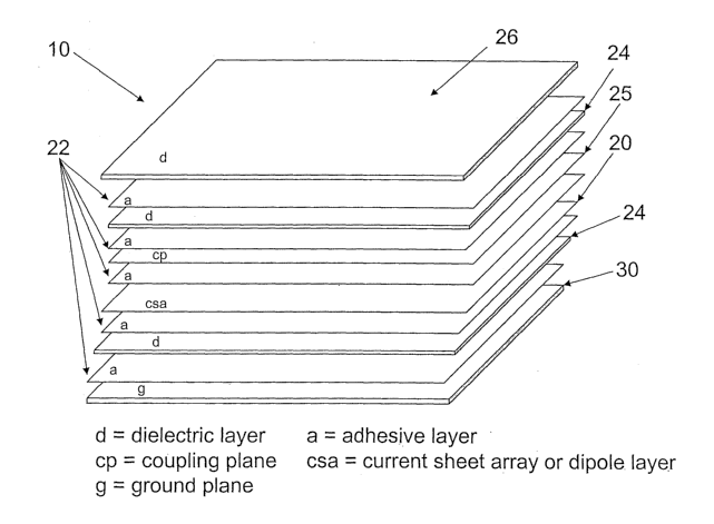
Referring initially to FIGS. 1 and 2(A-C), a
wideband phased array antenna 10 in accordance with the
present invention is illustrated. The antenna 10 may be
mounted on the nosecone 12, or other rigid mounting member
having either planar or a non-planar three-,dimensional shape,
of an aircraft or spacecraft, for example, and may also be
connected to a transmission and reception controller 14 as
would be appreciated by the skilled artisan.
The wideband phased array antenna 10 is preferably
formed of a plurality of flexible layers as shown in FIGS. 2A-
C. These layers include a dipole layer 20 or current sheet
array which is sandwiched between a ground plane 30 and an
outer dielectric layer 26 such as the outer dielectric layer
of foam shown. Other dielectric layers 24 (preferably made of
foam) may be provided in between as shown. Additionally, the
phased array antenna 10 further comprises at least one
coupling plane 25. It should be noted that the coupling plane
can be embodied in many different forms including planes that
are only partially metalized or fully metalized, coupling
planes that reside above or below the dipole layer 20, or
multiple coupling planes that can reside either above or below
the dipole layer or both. For example, antenna 10 of FIG. 2A
illustrates a coupling plane 25 that resides above the dipole
layer 20, whereas FIG. 2B illustrates a coupling plane 25
below the dipole layer 20. Antenna 10 of FIG, 2C illustrates
multiple coupling planes (25), one above and one below the
dipole layer 20. Each embodiment in FIG. 2 uses respective
adhesive layers 22 secure the dipole layer 20, ground plane
30, coupling plane 25, and dielectric layers of foam 24, 26
together to form the flexible and conformal antenna 10. Of
course other ways of securing the layers may also be used as
would be appreciated by the skilled artisan. The dielectric
layers 24, 26 may have tapered dielectric constants to improve
the scan angle. For example in FIG. 2A, the dielectric layer
CA 02508362 2005-06-O1
WO 2004/051791 PCT/US2003/037174
24 between the ground plane 30 and the dipole layer 20 may
have a dielectric constant of 3.0, the dielectric layer 24 on
the opposite side of the dipole layer 20 may have a dielectric
constant of 1.7, and the outer dielectric layer 26 may have a
dielectric constant of 1.2.
The current sheet array or dipole layer typically
consists of closely-coupled dipole elements embedded in
dielectric layers above a ground plane. Inter-element
coupling can be achieved with interdigital capacitors.
Coupling can be increased by lengthening the capacitor digits
as shown in FIGS. 6 and 7A. The additional coupling provides
more bandwidth. Unfortunately, sufficiently long digits will
exhibit a gain dropout, such as a 8dB gain dropout at l5GHz as
illustrated in the graph of FIG. 3. It is believed that the
capacitors tend to act as a bank of quarter-wave (~/4)
couplers. An E-field plot confirms that cross-polarized
capacitors are resonating at a dropout frequency even though
only vertically-polarized elements are fed into a particular
plot. Despite this, coupling must be maintained to extend the
bandwidth of a particular design. The present invention
maintains the necessary degree of inter-element coupling by
placing coupling plates on separate layers around or adjacent
to the interdigital capacitors. Shortening the capacitor
digits moves the gain dropout out of band, but reduces
coupling and bandwidth. Adding the coupling plates increases
the capacitive coupling to maintain or improve bandwidth. The
use of coupling plates improves bandwidth in simple designs
where no interdigital capacitors are used as shown in FIG. 7B.
A projected gain versus frequency plot exhibiting no in-band
gain notch is shown in FIG. 4 for an antenna using shorter
interdigital capacitors as illustrated in FIG. 7A. Likewise,
another projected gain versus frequency plot exhibiting no in-
band gain notch is shown in FIG. 5 for an antenna using no
interdigital capacitors as illustrated in FIG. 7B.
-g-
CA 02508362 2005-06-O1
WO 2004/051791 PCT/US2003/037174
Referring now to FIGS. 6, 7A and 7B, a first
embodiment of the dipole layer 20 will now be described. The
dipole layer 20 is a printed conductive layer having an array
of dipole antenna elements 40 on a flexible substrate 23. Each
dipole antenna element 40 can comprise a medial feed portion
42 and a pair of legs 44 extending outwardly therefrom.
Respective feed lines are connected to each feed portion 42
from the opposite side of the substrate 23, as will be
described in greater detail below. Adjacent legs 44 of
adjacent dipole antenna elements 40 have respective spaced
apart end portions 46 to provide increased capacitive coupling
between the adjacent dipole antenna elements. The adjacent
dipole antenna elements 40 have predetermined shapes and
relative positioning to provide the increased capacitive
coupling. For example, the capacitance between adjacent dipole
antenna elements 40 may be between about 0.016 and 0.636
picofarads (pF)', and preferably between 0.159 and 0.239 pF.
Preferably, as shown in FIG. 7A, the spaced apart
end portions 46 in adjacent legs 44 have overlapping or
interdigitated portions 47, and each leg 44 comprises an
elongated body portion 49, an enlarged width end portion 51
connected to an end of the elongated body portion, and a
plurality of fingers 53, for example four fingers extending
outwardly from the enlarged width end portion.
Alternatively, as shown in FIG. 7B, adjacent legs
44' of adjacent dipole antenna elements 40 may have respective
spaced apart end portions 46' to provide increased capacitive
coupling between the adjacent dipole antenna elements. In this
embodiment, the spaced apart end portions 46' in adjacent legs
44' comprise enlarged width end portions 51' connected to an
end of the elongated body portion 49' to provide the increased
capacitive coupling between the adjacent dipole antenna
elements. Here, for example, the distance K between the spaced
apart end portions 46' is about 0.003 inches. As shown in
-9-
CA 02508362 2005-06-O1
WO 2004/051791 PCT/US2003/037174
FIGS. 7A and 7B, coupling planes 25 illustrated in dashed
lines can reside adjacent to the dipole antenna elements
preferably above or below the dipole layer 20. The coupling
plane 25 can have metalization 27 on the entire surface of the
coupling plane as shown in FIG. 7A or metalization 27' on
select portions of the coupling plane as shown in FIG. 7B. Of
course, other arrangements which increase the capacitive
coupling between the adjacent dipole antenna elements are also
contemplated by the present invention.
Preferably, the array of dipole antenna elements 40
are arranged at a density in a range of about 100 to 900 per
square foot. The array of dipole antenna elements 40 are sized
and relatively positioned so that the wideband phased array
antenna 10 is operable over a frequency range of about 2 to 30
GHz, and at a scan angle of about ±60 degrees (low scan
loss). Such an antenna 10 may also have a 10:1 or greater
bandwidth, includes conformal surface mounting, while being
relatively lightweight, and easy to manufacture at a low cost.
For example, FIG. 7A is a greatly enlarged view
showing adjacent legs 44 of adjacent dipole antenna elements
40 having respective spaced apart end portions 46 to provide
the increased capacitive coupling between the adjacent dipole
antenna elements. In the example, the adjacent legs 44 and
respective spaced apart end portions 46 may have the following
dimensions: the length E of the enlarged width end portion 51
equals 0.061 inches; the width F of the elongated body
portions 49 equals 0.034 inches; the combined width G of
adjacent enlarged width end portions 51 equals 0.044 inches;
the combined length H of the adjacent legs 44 equals 0.276
inches; the width I of each of the plurality of fingers 53
equals 0.005 inches; and the spacing J between adjacent
fingers 53 equals 0.003 inches. In the example (referring to
FIG. 6), the dipole layer 20 may have the following
dimensions: a width A of twelve inches and a height B of
-10-
CA 02508362 2005-06-O1
WO 2004/051791 PCT/US2003/037174
eighteen inches. In this example, the number C of dipole
antenna elements 40 along the width A equals 43, and the
number D of dipole antenna elements along the length B equals
65, resulting in an array of 2795 dipole antenna elements.
The wideband phased array antenna 10 has a desired
frequency range, e.g. 2 GHz to 18 GHz, and the spacing between
the end portions 46 of adjacent legs 44 is less than about
one-half a wavelength of a highest desired frequency.
Referring to FIG. 8, another embodiment of the
dipole layer 20' may include first and second sets of dipole
antenna elements 40 which are orthogonal to each other to
provide dual polarization, as would be appreciated by the
skilled artisan
The phased array antenna 10 may be made by forming
the array of dipole antenna elements 40 on the flexible
substrate 23. This preferably includes printing and/or etching
a conductive layer of dipole antenna elements 40 on the
substrate 23. As shown in FIG. 8, first and second sets of
dipole antenna elements 40 may be formed orthogonal to each
other to provide dual polarization.
Again, each dipole antenna element 40 includes the
medial feed portion 42 and the pair of legs 44 extending
outwardly therefrom. Forming the array of dipole antenna
elements 40 includes shaping and positioning respective spaced
apart end portions 46 of adjacent legs 44 of adjacent dipole
antenna elements to provide increased capacitive coupling
between the adjacent dipole antenna elements. Shaping and
positioning the respective spaced apart end portions 46
preferably includes forming interdigitated portions 47 (FIG.
7A) or enlarged width end portions 51' (FIG. 7B). A ground
plane 30 is preferably formed adjacent the array of dipole
antenna elements 40, and one or more dielectric layers 24, 26
are layered on both sides of the dipole layer 20 with adhesive
layers 22 therebetween.
-11-
CA 02508362 2005-06-O1
WO 2004/051791 PCT/US2003/037174
Again, each dipole antenna element 40 includes the
medial feed portion 42 and the pair of legs 44 extending
outwardly therefrom. Forming the array of dipole antenna
elements 40 includes shaping and positioning respective spaced
apart end portions 46 of adjacent legs 44 of adjacent dipole
antenna elements to provide increased capacitive coupling
between the adjacent dipole antenna elements. Shaping and
positioning the respective spaced apart end portions 46
preferably includes forming interdigitated portions 47 (FIG.
7A) or enlarged width end portions 51' (FIG. 7B). A ground
plane 30 is preferably formed adjacent the array of dipole
antenna elements 40, and one or more dielectric layers 24, 26
are layered on both sides of the dipole layer 20 with adhesive
layers 22 therebetween.
As discussed above, the array of dipole antenna
elements 40 are preferably sized and relatively positioned so
that the wideband phased array antenna 10 is operable over a
frequency range of about 2 to 30 GHz, and operable over a scan
angle of about ±60 degrees. The antenna 10 may also be
mounted on a rigid mounting member 12 having a non-planar
three-dimensional shape, such as an aircraft, for example.
Thus, a phased array antenna 10 with a wide
frequency bandwith and a wide scan angle is obtained by
utilizing tightly packed dipole antenna elements 40 with large
mutual capacitive coupling. Conventional approaches have
sought to reduce mutual coupling between dipoles, but the
present invention makes use of, and increases, mutual coupling
between the closely spaced dipole antenna elements to prevent
grating lobes and achieve the wide bandwidth. The antenna 10
is scannable with a beam former, and each antenna dipole
element 40 has a wide beam width. The layout of the elements
could be adjusted on the flexible substrate 23 or printed
circuit board, or the bean former may be used to adjust the
path lengths of the elements to put them in phase.
-12-
CA 02508362 2005-06-O1
WO 2004/051791 PCT/US2003/037174
The present invention can be utilized in a
feedthrough lens as described in U.S. Patent No. 6,417,813 to
Timothy Durham, assigned to the assignee herein and hereby
incorporated by reference ('813 Patent). As described in the
'813 Patent, the feedthrough lens antenna may include first
and second phased array antennas (10) that are connected by a
coupling structure in back-to-back relation. Again, each of
the first and second phased array antennas are substantially
similar to the antenna 10 described above. The coupling
structure may include a plurality of transmission elements
each connecting a corresponding dipole antenna element of the
first phased array antenna with a dipole antenna element of
the second phased array antenna. The transmission elements may
be coaxial cables, for example, as illustratively shown in
FIG. 6 of the '813 Patent.
By using the wide bandwidth phased array antenna 10
described above, the feedthrough lens antenna of the present
invention will advantageously have a transmission passband
with a bandwidth on the same order. Similarly, the feedthrough
lens antenna will also have a substantially unlimited
reflection band, since the phased array antenna 10 is
substantially reflective at frequencies below its operating
band. Scan compensation may also be achieved. Additionally,
the various layers of the first and second phased array
antennas may be flexible as described above, or they may be
more rigid for use in applications where strength or stability
may be necessary, as will be appreciated by those of skill in
the art.
Whether the wideband phased array antenna 10 is used
by itself or incorporated in a feedthrough lens antenna, the
present invention can preferably be used with applications
requiring a continuous bandwidth of 9:1 or greater and
certainly extends the operational bandwidth of current sheet
arrays or dipole layers as described herein.
-13-