Note: Descriptions are shown in the official language in which they were submitted.
CA 02508651 2007-06-01
27986-22D
DESCRx PTx C> N
SCINTILLATOR PANEL AND RADIATION IMAGE SENSOR
Technical-Field
The present invention relates to a scintillator panel
and radiation image sensor used for medicalX-ray photography
and the like.
Background Art
Conventionally,X-ray, photosensitive f ilmshave been
used for medical and industrial X-ray photography. Flowever,. -
radiation imaging systems using radiation detectors have
come. into widespread use owing to advantages in convenience
and retention of photographic results. In.-such a radiation
1,5 imaging system, pixel data based on 2D-radiation is acquired
as an electrical signal by, the radiation detector, and th-e
signal is processed by the processor and displayed on the
monitor.
As a conventional, typical radiation detector, a
.20 radiation detector having a structure in which,an image
sensing element is stuck to a scintillator panel having a
scintillator formed on a substrate made of aluminum, glass,
molten quartz, or the like is available. In this radiation
detector, the scintillator converts radiation incident
25 from the substrate side into light, and'the. image sensing
element detects the light (see Japanese Patent Publication
No. 7021560) corresponding to U.S. Patent No. 5,153,438.
1
CA 02508651 2007-06-01
27986-22D
A radiation detector for medical purposes,
especially for dental examination, uses low-energy X-rays.
If, therefore, an aluminum substrate is used, quite a few
X-ray components are absorbed by the substrate. In a
radiation detector using low-energy X-rays, therefore, the
substrate of the scintillator panel is required to have high
radiation transmittance.
It is an object of the present invention to
provide a scintillator panel which increases the optical
output by using a substrate having high radiation
transmittance for the scintillator panel, and a radiation
image sensor using the scintillator panel.
Disclosure of Invention
According to a broad aspect, the invention
provides a scintillator panel comprising: a radiation
transmissive substrate; a scintillator supported by the
substrate, radiation passing through the substrate to enter
into the scintillator and light being generated in the
scintillator by the entered radiation; a transparent organic
protection film covering the scintillator, the light
generated in the scintillator passing through the
transparent organic protection film, wherein the substrate
is larger than the scintillator, wherein the transparent
organic protection film encapsulates the substrate and the
scintillator; and wherein the radiation passes through the
substrate to enter the scintillator, the scintillator
generates the light by the entered radiation, the generated
light emits from the transparent organic film covering the
scintillator toward to a side of the scintillator which is
opposite a side on which the scintillator is supported by
the substrate.
2
CA 02508651 2007-06-01
27986-22D
A scintillator panel of the present invention is
characterized by comprising a substrate substantially
consisting of carbon, a scintillator deposited on the
substrate, a protective film covering the scintillator.
According to this scintillator panel, since the
substrate substantially consisting of carbon has high
radiation transmittance, the amount of radiation absorbed by
the substrate can be decreased, and the amount of radiation
reaching the scintillator can be increased.
A radiation image sensor according to the present
invention is characterized by having an image sensing
element placed to oppose the scintillator of the
2a
CA 02508651 1999-04-09
27986-22D
scintillator panel comprising a substrate substantially
consisting of carbon, a scintillator deposited on the
substrate, and a protective film covering the scintillator.
According to this radiation image sensor, since
the scintillator panel has the substrate substantially
consisting of carbon having high radiation transmittance,
the amount of light reaching the image sensing element can
be increased.
Brief Description of Drawings
Fig. 1 is a sectional view of a scintillator panel
according to the first embodiment;
Fig. 2 is a sectional view of a radiation image
sensor according to the first embodiment;
Fig. 3A is a view showing the step in
manufacturing the scintillator panel according to the first
embodiment;
Fig. 3B is a view showing the step in
manufacturing the scintillator panel according to the first
embodiment;
Fig. 3C is a view showing the step in
manufacturing the scintillator panel according to the first
embodiment;
Fig. 3D is a view showing the step in
manufacturing the scintillator panel according to the first
embodiment;
Fig. 4 is a sectional view of a scintillator panel
according to the second embodiment;
3
CA 02508651 1999-04-09
27986-22D
Fig. 5 is a sectional view of a radiation image
sensor
3a
CA 02508651 1999-04-09
27986-22D
according to the second embodiment;
Fig. 6 is a sectional view of a scintillator panel
according to the third embodiment;
Fig. 7 is a sectional view of a radiation.image sensor
according to the third embodiment;
Fig. 8 is a sectional view of a scintillator panel
according to the fourth embodiment;
Fig. 9 is a sectional view of a radiation image sensor
according to the fourth embodiment; and
Fig. 10 is a view showing outputs from the radiation
image sensors according to the first to fourth embodiments
in comparison with outputs from the conventional radiation
image sensor.
Best Mode for Carrying Out the Invention
The first embodiment of the present invention will
be described below with reference to Figs. 1, 2, and 3A to
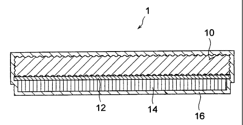
3D. Fig. 1 is a sectional view of a scintillator panel 1.
Fig. 2 is a sectional view of a radiation image sensor 2.
As shown in Fig . 1, the surfaces of an amorphous carbon
(a-C) (glassy carbon or glass-like carbon) substrate 10 have
undergone sandblasting, and an Al film 12 serving as a
reflecting film is formed on one surface. A columnar
scintillator 14 for converting incident 'radiation into
visible light is formed on the surface of the Al film 12.
Note that Tl-doped CsI is used for the scintillator 14. The
4
CA 02508651 1999-04-09
27986-22D
scintillator 14 is covered with a polyparaxylylene film 16,
together with the substrate 10.
As shown in Fig. 2, the radiation image sensor 2 has
a structure in which an image sensing element 18 is stuck
to the distal end side of the scintillator 14.
The steps in manufacturing the scintillator panel 1
will be described next with reference to Figs. 3A to 3D.
Sandblasting is performed on the surfaces of the rectangular
or circular a-C substrate 10 (thickness: 1 mm) by using glass
beads (#800). Fine projections/recesses are formed on the
surfaces of the substrate 10 by this sandblasting (see
Fig. 3A).
The Al film 12 serving as a reflecting film is then
formed on one surface of the substrate 10'to a thickness
of 100 nm by vacuum vapor deposition (see Fig. 3B). A
Tl-doped columnar CsI crystal is grown on the surface of
the Al film 12 by vapor deposition to form the scintillator
14 having a thickness of 250 ,um (see Fig. 3C).
CsI used to form this scintillator 14 has high
hygroscopicity, and hence absorbs water vapor from the air
and deliquesces if it is kept exposed to the air. In order
to prevent this, the polyparaxylylene film 16 is formed by
the CVD method . More specifically, the substrate 10 on which
the scintillator 14 is formed is placed in a CVD apparatus,
and the polyparaxylylene film .16 is formed to a thickness
of 10 um. With this process, the polyparaxylylene film
5
CA 02508651 1999-04-09
27986-22D
16 is formed on the entire surfaces of the scintillator 14
and substrate 10 (see Fig. 3D). Note that the formation
of the fine projections/recesses on the surfaces of the
substrate 10 by sandblasting can improve,the adhesion
characteristics between the polyparaxylylene film 16 and
the substrate 10, thus preventing peeling of the
polyparaxylylene film 16.
The radiation image sensor 2 is manufactured by
sticking the image sensing element (CCD) 18 to the distal
end portion side of the scintillator 14 of the completed
scintillator panel 1 such that the light-receiving portion
opposes the distal end portion side (see Fig. 2).
According to the radiation image sensor 2 of this
embodiment, radiation incident from the substrate 10 side
is converted into light by the scintillator 14 and detected
by the image sensing element 18. In this case, since a-C
substrate 10 has high radiation transmittance, the amount
of radiation absorbed by the substrate 10 can be reduced.
Hence, the amount of radiation reaching the scintillator
14 can be increased. In addition, since the Al film 12 as
a reflecting film is formed, light incident on the
light-receiving portion of the image sensing element 18can
be increased. This makes it possible to sharpen the image
detected by the radiation image sensor.
Fig. 10 shows outputs from the radiation image sensor
2 which are obtained when the radiation image sensor 2 detects
6
CA 02508651 1999-04-09
27986-22D
the X-rays generated by applying 40 kV, 50 kV, and 60 kV
as tube voltages to the half-wave rectifying X-ray tube,
in comparison with outputs from the conventional radiation
image sensor. More specifically, if the output obtained
when the conventional radiation image sensor detects the
X-ray generated by applying 40 kV as a tube voltage to the
half-wave rectifying X-ray:.tube is assumed to be 100%, the
output obtained when the X-ray is detected by the radiation
image sensor 2 is 260%. If the output obtained when the
conventional radiation image sensor detects the X-ray
generated by applying 50 kV as a tube voltage to the half-wave
rectifying X-ray tube is assumed to be 100%, the output
obtained when the X-ray is detected by the radiation image
sensor 2 is 230%. ~If the output obtained when the
conventional radiation image sensor detects the X-ray
generated by applying 60 kV as a tube voltage to the half-wave
rectifying X-ray tube is assumed to be 100%, the output
obtained when the X-ray is detected by the radiation image
sensor 2 is 220%.
The second embodiment of the present invention will
be described next. Note that the same reference numerals
denoting the parts of the scintillator panel 1 and radiation
image sensor 2 as in the first embodiment denote the same
parts in the second embodiment.
Fig. 4 is a sectional view of a scintillator panel
3. Fig. 5 is a sectional view of a radiation image sensor
7
CA 02508651 1999-04-09
27986-22D
4. As shown in Fig. 4, the surfaces of a-C substrate 10
of the scintillator panel 3 have undergone sandblasting,
and an Al film 12 serving as a reflecting film is formed"
on one surface. As a low-refractive-index member, an LiF
film (thin transparent film) 22 having a refractive index
(refractive index = 1.3) lower than that of a scintillator
14 is formed on the Al film 12. The columnar scintillator
14 for converting incident radiation into visible light is
formed on the surface of the LiF film 22. Note that Tl-doped
CsI (refractive index = 1.8) is used for the scintillator
14. The scintillator 14 is covered with a polyparaxylylene
film 16, together with the substrate 10.
As shown in Fig. 5, the radiation image sensor 4 has
a structure in which an image sensing element 18 is stuck
to the scintillator 14 side of the scintillator panel 3.
The steps in manufacturing the scintillator panel 3
will be described next. First of all, sandblasting is
performed on the surfaces of the rectangular or circular
a-C substrate 10 ( thickness : 1 mm) by using glass beads (#800),
thereby forming fine projections/recesses on the surfaces
of the substrate 10.
The Al film 12 serving as a reflecting film is then
formed on one surface of the substrate 10 to a thickness
of 100 nm by vacuum vapor deposition, and the LiF film 22
as a low-refractive-index member is formed on the Al film
12 to a thickness of 100 nm by vacuum vapor deposition. A
8
CA 02508651 1999-04-09
27986-22D
T1-doped columnar CsI crystal is grown on the surface of
the LiF film 22 by vapor deposition to form the scintillator
14 having a thickness of 250 ,um. The polyparaxylylene film
16 is formed to a thickness of 10 ,um by the CVD method.
With this process, the polyparaxylylene film 16 is formed
on the entire surfaces of the scintillator 14 and substrate
10.
The radiation image sensor 4 is manufactured by
sticking the image sensing element ( CCD ) 18 to the distal
end portion of the scintillator 14 of the completed
scintillator panel 3 such that the light-receiving portion
opposes the distal end portion (see Fig. 5).
According to the radiation image sensor 4 of this
embodiment, radiation incident from the substrate 10 side
is converted into light by the scintillator 14 and detected
by the image sensing element 18. In this case, since a-C
substrate 10 has high radiation transmittance, the amount
of radiation absorbed by the substrate 10 can be reduced.
Hence, the amount of radiation reaching the scintillator
14 can be increased. In addition, since the Al film 12 as
a reflecting film and the LiF film 22 as a
low-refractive-index member are formed, light incident on
the light-receiving portion of the image sensing element
18 can be increased. This makes it possible to sharpen the
image detected by the radiation image sensor.
As shown in Fig. 10, if the output obtained when the
9
CA 02508651 1999-04-09
2798b-22D
conventional radiation image sensor detects the X-ray
generated by applying 40 kV as a tube voltage to the half-wave
rectifying X-ray tube is assumed to be 100%, the output
obtained when the X-ray is detected by the radiation image
sensor 4 is 300%. If the output obtained when the
conventional radiation image sensor detects the X-ray
generated by applying 50 kV as a tube voltage to the half-wave
rectifying X-ray tube is assumed to be 100%, the output
obtained when the X-ray is detected by the radiation image
sensor 4 is 270%. If the output obtained when the
conventional radiation image sensor detects the X-ray
generated by applying 60 kV as a tube voltage to the half-wave
rectifying X-ray tube is assumed to be 100%, the output
obtained when the X-ray is detected by the radiation image
sensor 4 is 260%.
The third embodiment of the present invention will
be described next. Note that the same reference numerals
denoting the parts of the scintillator panels 1 and 3 and
radiation image sensors 2 and 4 as in the first and second
embodiments denote the same parts in the third embodiment.
Fig. 6 is a sectional view of a scintillator panel
5. Fig. 7 is a sectional view of a radiation image sensor
6. As shown in Fig. 6, the surfaces of a-C substrate 10
of the scintillator panel 3 have undergone sandblasting,
and an LiF f ilm (thin transparent f ilm ) 22 is f ormed on one
surface. A columnar scintillator 14 for converting
CA 02508651 1999-04-09
27986-22D
incident radiation into visible light is formed on the
surface of the LiF film 22. Note that Tl-doped CsI is used
for the scintillator 14. The scintillator 14 is covered
with a polyparaxylylene film 16, together with the substrate
10.
As shown in Fig. 7, the radiation image sensor 6 has
a structure in which an image sensing element 18 is stuck
to the distal end portion side of the scintillator 14 of
the scintillator panel 5.
The steps in manufacturing the scintillator panel 5
will be described next. First of all, sandblasting is
performed on the surfaces of the rectangular or circul'ar
a-C substrate 10 ( thickness : 1 mm ) by us ing glass beads (#800),
thereby forming fine projections/recesses on the surfaces
of the substrate 10.
The LiF film 22 as a low-refractive-index member is
then formed on one surface of the substrate 10 to a thickness
of 100 nm by vacuum vapor deposition. A Tl-doped columnar
CsI crystal is grown on the surface of the LiF film 22 by
vapor deposition to form the scintillator 14 having a
thickness of 250 CCm. The polyparaxylylene film 16 is formed
to a thickness of 10 ,um by the CVD method. With this p'rocess,
the polyparaxylylene film 16 is formed on the entire surfaces
of the scintillator 14 and substrate 10.
The radiation image sensor 6 is manufactured by
sticking the image sensing element ( CCD ) 18 to the distal
I1
CA 02508651 1999-04-09
27986-22D
end portion side of the scintillator 14 of, the completed
scintillator panel 5 such that the light-receiving portion
opposes the distal end portion side (see Fig. 7).
According to the radiation image sensor 6 of this
embodiment, radiation incident from the substrate 10 side
is converted into light by the scintillator 14 and detected
by the image sensing element 18. In this case, since a-C
substrate 10 has high radiation transmittance, the amount
of radiation absorbed by the substrate 10 can be reduced.
Hence, the amount of radiation reaching the scintillator
14 can be increased. In addition, since the LiF film 22
is formed as a low-refractive-indexmember, light satisfying
the total reflection condition is reflected by the interface
between the scintillator 14 and the LiF film 22, and the
amount of light incident on the light-receiving portion of
the image sensing element 18 can be increased. This makes
it possible to sharpen the image detected by the radiation
image sensor.
As shown in Fig. 10, if the output obtained when the
conventional radiation image sensor detects the X-ray
generated by applying 40 kV as a tube voltage to the half-wave
rectifying X-ray tube is assumed to be 100%, the output
obtained when the X-ray is detected by the radiation image
sensor 6 is 220%. If the output obtained when the
conventional radiation image sensor detects the X-ray
generated by applying 50 kV as a tube voltage to the half-wave
12
CA 02508651 1999-04-09
27986-22D
rectifying X-ray tube is assumed to be 100%, the output
obtained when the X-ray is detected by the radiation image
sensor 6 is 200%. If the output obtained when the
conventional radiation image sensor detects the X-ray
generated by applying 60 kV as a tube voltage to the half-wave
rectifying X-ray tube is assumed to be 100%, the output
obtained when the X-ray is detected by the radiation image
sensor 6 is 190%.
The fourth embodiment of the present invention will
be described next. Note that the same reference numerals
denoting the parts of the scintillator panel 1 and radiation
image sensor 2 as in the first embodiment denote the same
parts in the fourth embodiment.
Fig. 8 is a sectional view of a scintillator panel
7. Fig. 9 is a sectional view of a radiation image sensor
8. As shown in Fig. 8, one surface and side surfaces of
a-C substrate 10 of the scintillator panel 7 have undergone
sandblasting, and the other surface is mirror-polished.
A columnar scintillator 14 for converting incident
radiation into visible light is formed on the other surface
of this substrate. Note that Tl-doped CsI is used for the
scintillator 14. The scintillator 14 is covered with a
polyparaxylylene film 16, together with the substrate 10.
As shown in Fig. 9, the radiation image sensor 8 has
a structure in which an image sensing element 18 i's stuck
to the scintillator 14 side of the scintillator panel 7.
13
CA 02508651 1999-04-09
27986-22D
The steps in manufacturing the scintillator panel 7
will be described next. First of all, sandblasting is
performed on the surfaces of the rectangular or circular
a-C substrate 10 ( thickness : 1 mm) by using glass beads (#800),
thereby forming fine projections/recesses on the surfaces
of the substrate 10. In addition, the other surface of the
substrate 10 is mirror-polished.
A Tl-doped columnar CsI crystal is grown on the other
surface of the substrate 10 by vapor deposition to form the
scintillator 14 having a thickness of 250 ,Um.. The
polyparaxylylene film 16 is formed to a thickness of 10
m by the CVD method. With this process, the polyparaxylylene
film 16 is formed on the entire surfaces of the scintillator
14 and substrate 10.
The radiation image sensor 8 is manufactured by
sticking the image sensing element (CCD) 18 to the distal
end portion side of the scintillator 14 of the completed
scintillator panel 7 such that the light-receiving portion
opposes the distal end portion side (see Fig. 9).
According to the radiation image sensor 8 of this
embodiment, radiation incident from the substrate 10 side
is converted into light by the scintillator 14 and detected
by the image sensing element 18. In this case, since a-C
substrate 10 has high radiation transmittance, the amount
of radiation absorbed by the substrate 10 can be reduced.
Hence, the amount of radiation reaching the scintillator
14
CA 02508651 1999-04-09
27986-22D
14 can be increased. This can increase the amount of light
incident on the light-receiving portion of the image sensing
element 18, thereby sharpening the image detected by the
radiation image sensor B.
As shown in Fig. 10, if the output obtained when the
conventional radiation image sensor detects the X-ray
generated by applying 40 kV as a tube voltage to the half-wave
rectifying X-ray tube is assumed to be 100%, the output
obtained when the X-ray is detected by the radiation image
sensor 8 is 150%. If the output obtained when the
conventional radiation image sensor detects the X-ray
generated by applying 50 kV as a tube voltage to the half-wave
rectifying X-ray tube is assumed to be 100%, the output
obtained when the X-ray is detected by the radiation image
sensor 8 is 135%. If the output obtained when the
conventional radiation image sensor detects the X-ray
generated by applying 60 kv as a tube voltage to the half-wave
rectifying X-ray tube is assumed to be 100%, the output
obtained when the X-ray is detected by the radiation image
sensor 8 is 130%.
in each embodiment described above, the a-C substrate
is used. However, a graphite substrate may be used. The
graphite substrate has high radiation transmittance like
the a-C substrate. In this case, therefore, the amount of
radiation reaching the scintillator can be increased as in
the case wherein the a-C substrate is used.
CA 02508651 1999-04-09
27986-22D
In the above embodimeiits, a LiF film is used as a thin
transparent film. However, a film made of a material
containing selected from the group consisting of LiF, MgF21
CaFZ1 Si02, A1203, MgO, NaCl, KBr, KC1, and AgCl may be used.
In each embodiment described above, CsI (Tl) is used
as the scintillator 14. However, the present invention is
not limited to this. For example,CsI(Na),NaI(Tl),LiI(Eu),
or KI(T1) may be used.
In each embodiment described above, examples of the
polyparaxylylene are polymonochloroparaxylylene,
polydichloroparaxylylene, polytetrachloroparaxylylene,
polyfluoroparaxylylene, polydimethylparaxylylene, and
polydiethylparaxylylene.
According to the scintillator panel of the present
invention, since the substrate made of carbon as a major
constituent has high radiation transmittance, the amount
of radiation absorbed by the substrate can be decreased,
and the amount of radiation reaching the scintillator*can
be increased.
In addition, according to the radiation image sensor
of the present invention, since the scintillator panel has
the substrate made of carbon as a major constituent having
high radiation transmittance, the amount of light reaching
the image sensing element can be increased.
Industrial Applicability
As described above, the scintillator panel and
16
CA 02508651 1999-04-09
27986-22D
radiation image sensor of the present invention are suited
for medical X-ray photography and the like.
17