Note: Descriptions are shown in the official language in which they were submitted.
CA 02508889 2005-06-06
WO 2004/061762 PCT/US2003/034921
A TAMPER-INDICATING RFID ANTENNA
s
TECHNICAL FIELD
l0 The present invention relates to a tamper-indicating radio frequency
identification
device made of densified metal powder and to a sticker including the same
antenna. The
present invention also relates to radio frequency identification antenna made
of densified
metal powder and to a sticker including the same antenna. The present
invention also
relates to methods of indicating that a radio frequency identification antenna
or sticker has
is been tampered with.
BACKGROUND OF THE INVENTION
Radio frequency identification technology has become widely used in virtually
every industry, including transportation, manufacturing, waste management,
postal
20 tracking, airline baggage reconciliation, and highway toll management. An
RFID system
is made up of two components, the transponder and the interrogator or reader.
The
essential components of a transponder are the data carrying device - generally
referred to
as an integrated circuit or an electronic microchip, and a coupling element -
such as an
antenna. A transponder that contains its own power supply, generally a
battery, is know as
2s an active tag, while a transponder that does not contain its own power
supply is known as
a passive tag, sticker or label. The interrogator or reader contains a radio
frequency
module (transmitter and receiver), a control unit and a coupling element - an
antenna.
Power and data exchange between the transponder and the interrogator are
achieved
through magnetic or electromagnetic fields.
30 An example of a radio frequency identification sticker is disclosed in U.S.
Patent
No. 6,121,880 (Scott et al.), "Sticker Transponder for Use on Glass Surface."
This patent
discloses a sticker transponder adapted to be affixed to a glass surface, such
as a vehicle
windshield, including a RFID transponder enabling the storage and retrieval of
vehicle
related data. The sticker transponder comprises a flexible circuit substrate
having an
3s antenna formed thereon and a transponder circuit disposed on the substrate
and coupled to
-1-
CA 02508889 2005-06-06
WO 2004/061762 PCT/US2003/034921
the antenna. An adhesive layer is coupled to a first surface of the flexible
circuit substrate.
An indicia layer is coupled to a second surface of the flexible circuit
opposite from the
first surface. The indicia layer comprises a space permitting indicia to be
printed thereon.
The antenna has a characteristic impedance defined in part by a dielectric
constant of the
glass surface. As a result, a proper impedance match between the antenna and
the
transponder circuit is achieved only when the sticker is affixed to the glass
surface. The
sticker transponder further comprises a release liner affixed to the adhesive
layer, the
release liner being selectively removable to permit the sticker transponder to
be affixed to
the glass surface. The transponder circuit further includes a memory having a
read-only
1o portion and a re-writable portion.
An example of a tamper indicating radio frequency identification label is
disclosed
in PCT Publication WO 01/71848A1 (Atherton), "A Tamper Indicating Radio
Frequency
Identification Label." This publication discloses a label which may include
RFID
components and a tamper track coupled to the RFID components. The tamper track
should be constructed from a destructible conducting path. Additionally, the
tamper rack
can be formed such that it is damaged when the label is tampered: In one
embodiment,
adhesion characteristics of the tamper track (102) are adapted to break apart
the tamper
track when the label is tampered, for example, by removal from an object. The
RFID
components may retain their RF capability and detect when the tamper track
(102) has
2o been damaged to indicate that the label has been tampered. Alternatively,
the RFC
capability of the RFID components may be disabled when the tamper track is
damaged,
indicating tampering.
SUMMARY OF THE INVENTION
One aspect of the present invention provides a tamper-indicating radio
frequency
identification device. The radio frequency identification device comprises: a
substrate
including a first major surface and a second major surface opposite the first
major surface;
and a radio frequency identification antenna attached to the first major
surface of the
substrate, where said antenna comprises densified metal powder. In one
preferred
embodiment of the above tamper-indicating radio frequency identification
device, the
antenna responds to a signal, and after the tamper-indicating radio frequency
identification
antenna is bent equal to or less than a radius of 25 mm, the tamper-indicating
radio
frequency identification antenna does not respond to the signal.
-2-
CA 02508889 2005-06-06
WO 2004/061762 PCT/US2003/034921
Another aspect of the present invention provides a tamper-indicating radio
frequency identification sticker. The tamper-indicating radio frequency
identification
sticker comprises: a substrate including a first major surface and a second
major surface
opposite the first major surface; and a radio frequency identification antenna
attached to
the first major surface of the substrate, where said antenna comprises
densified metal
powder; a first integrated circuit attached to the antenna; and a first layer
of adhesive
attached to the substrate. In one preferred embodiment of the above tamper-
indicating
radio frequency identification sticker, the antenna responds to a signal, and
after the
tamper-indicating radio frequency identification antenna is bent equal to or
less than a
to radius of 25 mm, the tamper-indicating radio frequency identification
antenna does not
respond to the signal.
Another aspect of the present invention provides a method of indicating that a
radio frequency identification sticker has been tampered. The method comprises
the steps
of: attaching a tamper-indicating radio frequency identification sticker to a
first surface,
where the tamper-indicating radio frequency identification sticker, comprises:
a substrate
including a first major surface and a second major surface opposite the first
major surface;
and a radio frequency identification antenna attached to the first major
surface of the
substrate, where said antenna comprises densified metal powder; a first
integrated circuit
attached to the antenna; and a first layer of adhesive attached to the
substrate; sending a
2o signal to the tamper-indicating radio frequency identification sticker
attached to the first
surface; receiving a response from the antenna, removing the tamper-indicating
radio
frequency identification sticker from the first surface; and sending the
signal to the
tamper-indicating radio frequency identification sticker and not receiving a
response from
the antenna. In one preferred embodiment of the above method, the removing
step
comprises bending the tamper-indicating radio frequency identification antenna
less than
or equal to a radius of 25 mm.
Yet another aspect of the present invention provides an alternative method of
indicating a radio frequency identification sticker has been tampered. This
method
comprises the steps of: attaching a tamper-indicating radio frequency
identification sticker
to a first surface, where the tamper-indicating radio frequency identification
sticker,
comprises: a substrate including a first major surface and a second major
surface opposite
the first major surface; and a radio frequency identification antenna attached
to the first
-3-
CA 02508889 2005-06-06
WO 2004/061762 PCT/US2003/034921
major surface of the substrate, where said antenna comprises densified metal
powder; a
first integrated circuit attached to the antenna; and a first layer of
adhesive attached to the
substrate; measuring a first resistance in the antenna; bending the tamper-
indicating radio
frequency identification sticker less than or equal to a radius of 25 mm; and
measuring a
second resistance in the antenna that is higher than the first resistance of
the antenna.
Another aspect of the present invention provides another alternative method of
indicating a radio frequency identification sticker has been tampered. This
method
comprises the steps of: attaching a tamper-indicating radio frequency
identification sticker
to a first surface, where the tamper-indicating radio frequency identification
sticker,
to comprises: a substrate including a first major surface and a second major
surface opposite
the first major surface; and a radio frequency identification antenna attached
to the first
major surface of the substrate, where said antenna comprises densified metal
powder; a
first integrated circuit attached to the antenna; and a first layer of
adhesive attached to the
substrate; measuring a first conductivity in the antenna; bending the tamper-
indicating
radio frequency identification sticker less than or equal to a radius of 25
mm; and
measuring a,second conductivity in the antenna that is lower than the first
conductivity of
the antenna.
Another aspect of the present invention provides yet another alternative
method of
indicating a radio frequency identification sticker has been tampered. This
method
2o comprises the steps of: attaching a tamper-indicating radio frequency
identification sticker
to a first surface, where the tamper-indicating radio frequency identification
sticker,
comprises: a substrate including a first major surface and a second major
surface opposite
the first major surface; and a radio frequency identification antenna attached
to the first
major surface of the substrate, where said antenna comprises densified metal
powder; a
first integrated circuit attached to the antenna; and a first layer of
adhesive attached to the
substrate; measuring a first conductivity in the antenna; bending the tamper-
indicating
radio frequency identification sticker less than or equal to a radius of 25
mm; and
measuring a second conductivity that indicates that the antenna is
nonconductive.
Another aspect of the present invention provides another alternative method of
indicating a radio frequency identification sticker has been tampered. This
method
comprises the steps of: attaching a tamper-indicating radio frequency
identification sticker
to a first surface, where the tamper-indicating radio frequency identification
sticker,
-4-
CA 02508889 2005-06-06
WO 2004/061762 PCT/US2003/034921
comprises: a substrate including a first major surface and a second major
surface opposite
the first major surface; and a radio frequency identification antenna attached
to the first
major surface of the substrate, where said antenna comprises densified metal
powder; a
first integrated circuit attached to the antenna; and a first layer of
adhesive attached to the
substrate; bending the tamper-indicating radio frequency identification
sticker less than or
equal to a radius of 25 mm; and forming a fracture in the radio frequency
identification
antenna.
Another aspect of the present invention provides another alternative method of
indicating a radio frequency identification sticker has been tampered. The
method
to comprises the steps of: attaching a tamper-indicating radio frequency
identification sticker
to a first surface, where the tamper-indicating radio frequency identification
sticker,
comprises: a substrate including a first major surface and a second major
surface opposite
the first major surface; and a first radio frequency identification antenna
attached to the
first major surface of the substrate, where said antenna comprises densified
metal powder;
a first integrated circuit attached to the antenna; a second integrated
circuit attached to the
substrate, where the second integrated circuit comprises a second antenna; and
a first layer
of adhesive attached to the substrate; sending a signal to the tamper-
indicating radio
frequency identification sticker attached to the first surface; receiving a
response from the
first antenna and the second antenna; removing the tamper-indicating radio
frequency
2o identification sticker from the first surface; sending the signal to the
tamper-indicating
radio frequency identification sticker; and receiving a signal from the second
antenna and
not receiving a response from the first antenna.
Another aspect of the present invention provides a tamper-indicating radio
frequency identification sticker. The tamper-indicating radio frequency
identification
sticker comprises: a substrate including a first major surface and a second
major surface
opposite the first major surface, where the substrate is selected from the
group consisting
of paper and materials that are at least about 10% compressible, and where the
materials
that are at least 10% compressible are selected from the group consisting of
microporous
materials, nonwoven materials and woven materials; and a radio frequency
identification
loop antenna attached to the first major surface of the substrate, where said
antenna
comprises densified metal powder, where the densified metal powder is selected
from the
group consisting of copper, tin, lead, silver, gold, platinum, aluminum,
nickel, iron, steel,
-5-
CA 02508889 2005-06-06
WO 2004/061762 PCT/US2003/034921
zinc and alloys and combinations thereof; and where the metal powder comprises
metal
particles in the shape of spheres, oblongs, and polyhedra; a first integrated
circuit attached
to the antenna; and a first layer of adhesive attached to the substrate; where
the antenna
responds to a signal sent a distance greater than 15 cm from the tamper-
indicating radio
frequency identification sticker, and where after the tamper-indicating radio
frequency
identification sticker is bent equal to or less than or equal to a radius of
25 mm, the
tamper-indicating radio frequency identification antenna does not respond to
the signal
and the antenna comprises a fracture that is not visible to the naked eye.
Yet another aspect of the present invention provides a radio frequency
identification antenna. The radio frequency identification antenna comprises:
a substrate
including a first major surface and a second major surface opposite the first
major surface;
and a radio frequency identification antenna attached to the first major
surface of the
substrate, where said antenna comprises densified metal powder.
The details of one or more embodiments of the invention are set forth in the
accompanying drawings and the description below. Other features, objects, and
advantages of the invention will be apparent from the description and
drawings, and from
the claims.
BRIEF DESCRIPTION OF THE DRAWINGS
2o The present invention will be further explained with reference to the
appended
Figures, wherein like structure is referred to by like numerals throughout the
several
views, and wherein:
Figure 1 is a top view of one embodiment of a radio frequency identification
device;
Figure 2 is a top view of one embodiment of a tamper-indicating radio
frequency
identification sticker including the device of Figure 1;
Figure 3a is cross-sectional view of the tamper-indicating radio frequency
identification sticker of Figure 2 taken along line 3 in Figure 2;
Figure 3b is cross-sectional view of another embodiment of the tamper-
indicating
3o radio frequency identification sticker taken along line 3 in Figure 2;
-6-
CA 02508889 2005-06-06
WO 2004/061762 PCT/US2003/034921
Figure 4a is cross-sectional view of the tamper-indicating radio frequency
identification sticker of Figure 2 applied to a surface and a portion of the
sticker is bent at
a radius Rl;
Figure 4b is cross-sectional view of the tamper-indicating radio frequency
identification sticker of Figure 4a a portion of the sticker is bent at a
radius R2, taken along
line 4b in Figure 6a;
Figure 5a is a cross-sectional view of an alternative embodiment of the tamper-
indicating radio frequency identification sticker taken along line 5 in Figure
2;
Figure 5b is a cross-sectional view of another alternative embodiment of the
to tamper-indicating radio frequency identification sticker taken along line 5
in Figure 2;
Figure 6a is a top view of the tamper-indicating radio frequency
identification
sticker of Figure 4b with the adhesive layer removed for clarity; and
Figure 6b a top view of another embodiment of a tamper-indicating radio
frequency identification sticker with the adhesive layer removed for clarity.
DETAILED DESCRIPTION OF THE INVENTION
Figure 1 illustrates one preferred embodiment of a radio frequency
identification
("RF117") device 10. The RFID device 10 includes a substrate 14, which has a
first major
surface 16 and a second major surface 18 opposite the first major surface
(shown in Figure
3a). The substrate 14 is preferably a compressible material. As used herein,
compressible
means that a substrate reduces in its dimension parallel to an applied
pressure and that the
total volume of the substrate is also reduced by a similar amount. When used
herein as a
quantitative measure, X % compressible means that the dimension of a substrate
measured
parallel to an applied pressure of 30 MPa is [(100-X)/100] times its dimension
in this
direction at 0.07 MPa and the total volume of the substrate at 30 MPa is [(100-
X)/100]
times its volume at 0.07 MPa. If the dimension change in the direction of the
applied
pressure and the volume change yield different values of X, then the smaller X
of the two
values is used to define the quantitative compressibility of the material.
Preferably,
following release of an applied pressure, substrates 14 still show dimension
and volume
3o changes of at least 10%, more preferably they show dimension and volume
changes that
_7_
CA 02508889 2005-06-06
WO 2004/061762 PCT/US2003/034921
are at least 50% of the percent compressibility observed at 30 MPa, and most
preferably
they maintain dimension and volume changes that are at least 75 % of the
percent
compressibility achieved at 30 MPa.
Preferably, substrate 14 is made of paper and compressible fibrous and non-
fibrous
materials, including those manufactured from synthetic or naturally occurring
polymers, or
- combinations thereof. Suitable forms of these substrates include nonwovens
including
dry-lay and wet-lay nonwovens, nonwovens made by melt-blown fiber, spun bond
or spun
lace processes, woven and knit fabrics, membranes, foams (preferably open-cell
foams)
and expanded webs, and webs comprised of cast fibers.
l0 Paper is one preferred substrate 14 and a variety of papers are suitable,
including,
but not limited to, kraft paper, stationery paper, copier paper, filter paper,
newsprint,
cardstock, folder stock, printing paper, specialty papers, paper products such
as pulp board
and the like. Suitable papers may be made by various processes and may contain
fillers,
sizing agents, pigments, dyes, and others additives as known to those skilled
in the art.
Suitable papers may be calendered or non-calendered, processed to provide
various
finishes and coated or uncoated.
Suitable nonwoven substrates can include membranes or porous materials, such
as,
for example, ultrafiltration membranes, microporous materials, cast polymeric
membranes, and thermally induced phase transition materials (TIPS), which are
described
in U.S. Pat. Nos. 4,247,498 and 4,867,881. One suitable substrate is a
particle-filled,
microporous material, commercially available from PPG Industries, Pittsburgh,
PA, under
the trade designation Teslin. Teslin is described by its manufacturer as a
dimensionally
stable, polyolefin based, microporous, printing sheet with 60% of its weight
including a
non-abrasive filler and with 65% of its volume including air.
Suitable substrate materials may be fibrous and fiber-like materials including
silk
and cellulosic or lignocellulosic materials, such as for example, flax, hemp,
cotton, jute, or
synthetic cellulosic or lignocellulosic materials such as rayon.
Suitable substrates can be made from a variety of polymers, including
thermoplastic, thermoset, elastomeric, and crosslinked polymers. Examples of
suitable
polymers include polyamides, polyurethanes, polyolefins (e.g., polyethylene
and
polypropylene), polystyrene, polycarbonate, polyethers, polyvinylchloride,
silicones,
_g_
CA 02508889 2005-06-06
WO 2004/061762 PCT/US2003/034921
fluoropolymers, polysulfones, nylons, cellulose acetate, ethylenically
unsaturated
polymers, and suitable combinations thereof.
RFm device 10 includes a densified metal powder layer 12. The densified metal
powder layer 12 in Figure 1 is illustrated in a pattern of a loop. However,
the densified
metal powder layer may be in any pattern. The pattern of densified metal
powder layer 12
is formed on the substrate by at least one of the methods taught in U.S.
Patent Application
Serial No. 09/952,239, "Method for Making Conductive Circuits Using Powdered
Metals,
" (Koskenmaki et al.), filed on ) September 10, 2001, the entirety of which is
hereby
incorporated by reference, and which is co-owned by the assignee of the
present invention.
l0 To summarize at least one of these methods described in this application,
the densified
metal powder layer 12 is formed on the substrate 14 by a multiple step
process. First, a
metal powder composition is deposited onto the substrate 14. Second, a capture
process
step is performed by applying pressure to the powder composition and substrate
with a
hydraulic press with a die having projections or male portions against a
platen. The
projections of die are shaped to produce a patterned layer of densified metal
powder 12 in
the plane of the substrate 14. Any pattern may be machined onto the die and
thereby
imparted to metal powder composition on substrate 14. During this capture
step, the
captured metal powder composition is formed into a pattern and adheres to the
substrate
14, while the metal powder composition outside the projections remains
uncaptured. The
processing conditions used to capture the pattern of densified metal powder 12
will vary
widely depending on the metal powders selected for use in the metal powder
composition,
as well as the properties of the substrate material. Temperatures, pressures
and application
times should be selected to substantially minimize, and preferably eliminate,
damage to
the substrate 14, such as melting, warping, buckling, blistering, or
decomposing.
Preferably, the platen is maintained at a temperature between 50 and -
25°C, and the die or
at least the raised portions of the die, are maintained at a temperature
between 20 and 250
°C, preferably between 20 and 200°C. Useful processing pressure
is in the range of 20
MPa to 400 MPa, and pressure is maintained for up to 300 seconds. Preferably,
the platen
and the die are maintained at about 20 to 25°C, and a pressure between
about 35 MPa and
200 MPa is maintained for no more than about 60 seconds.
Third, the residual, unadhered metal powder composition that is uncaptured may
optionally be substantially removed from the substrate by a variety of
conventional
-9-
CA 02508889 2005-06-06
WO 2004/061762 PCT/US2003/034921
methods, for example, compressed air, vacuum, vibration, brushing, blowing,
gravity,
aqueous wash, and suitable combinations thereof.
Fourth, a densifying energy in the form of a second pressure is then applied
with
platens to the pattern of densified metal powder layer 12 to densify the
pattern.
Preferably, this densifying process step increases the adhesion of the pattern
to the
substrate 14 and makes the pattern more conductive. The second pressure may be
applied
as hydraulic pressure, and optionally heat, acoustic or microwave energy may
be
simultaneously or subsequently applied. Ultrasonic energy, heat or microwave
energy
may also be employed prior to the application of pressure, or may be employed
alone to
to accomplish densification without the application of a second pressure. The
densification
step may be performed in a continuous process by such means, for example, as
calendar
rolls, a hot zone or a sonication zone, or in a batchwise or step-and-repeat
process using,
for example, a hydraulic press, a thermal or microwave oven, or an ultrasonic
horn.
Densification means that the metal particles have been compressed together
with such
high pressures that the'metal particles are mechanically joined together very
tightly, to the
point where some of the particles may even be cold-welded together, but
notairltered or .
annealed.
The pressure applied in the densification step is about 20 MPa to about 400
MPa,
preferably about 60 MPa to 200 MPa. Densification at these pressures is
conducted at
temperatures from about 20°C to 250°C, preferably about
50°C to 200°C. most preferably
about 100°C to about 150°C. With application of other sources of
densifying energy such
as ultrasonic energy, different temperatures ranges may be preferred.
Lastly, the platen is removed, resulting in the RFID device 10 illustrated in
Figure
1 having a conductive metal pattern of densified metal powder layerl2 adhered
on the first
major surface 16 of the substrate 14.
The metal powder composition used to make the densified metal powder layer 12
described above preferably includes finely divided metal particles. The metal
particles
suitable for use in the metal powder composition include copper, tin, nickel,
iron, steel,
platinum, aluminum, silver, gold, lead, zinc and the like, and copper is
particularly
preferred. The metal powder composition may also include conductive non-metal
powders, such as, for example, graphite. The metal powder composition may
contain only
-10-
CA 02508889 2005-06-06
WO 2004/061762 PCT/US2003/034921
one metal or it may contain two or more metals, in such combinations as a
mixture of
particles of two or more metals, particles comprising alloys, blends or
mixtures, particles
of one metal coated with a second metal, and the like. The shape of the
particles in the
metal powder composition can vary widely. The metal particles can be of the
same shape
or of different shapes and can be regularly or irregularly shaped. Exemplary
particle
shapes include, for example, spheres, oblongs, needles, dendrites, polyhedra
(e.g.,
tetragons, cubes, pyramids and the like), prisms, flakes, rods, plates,
fibers, chips,
whiskers, and mixtures thereof. Similarly, the sizes of the metal particles in
the metal
powder composition can vary widely, and may include monodisperse particles, a
multi-
modal distribution of particle sizes, or a broad distribution of particle
sizes. Preferably,
the particles in the metal powder composition have a mean particle size of
approximately
0.1 to about 2000 um; preferably between about 0.2 um and about 1000 um; most
preferably between about 1 um and about 500 um.
For the tamper-indicating feature of one of the present inventions, as
explained
below in reference to Figures 4a-4b, it is preferable to form densified metal
powder layers
which have reduced flexibility and may easily crack or fracture, especially
upon bending.
To achieve this feature, the metal powder compositions preferably include
particle shapes
which will more easily mechanically separate from each other or become
undensified
when the densified metal powder layer 12 (or the entire device 10) is bent at
a radius less
2o than or equal to 25 mm. For example, metal particles in the shape of
spheres will most
easily mechanically separate from each other or easily crack or fracture due
to their
smooth, round shape. In sharp contrast,densified metal powders made solely of
metal
particles only in the shape of dendrites (shaped like branches or trees) will
tend to stay
mechanically joined together and tend not to crack or fracture due to their
ability to fasten
together, even if the antenna is bent at a radius less than or equal to 25 mm.
Metal
powders in the shape of oblongs and polyhedra tend to easily mechanically
separate from
each other or easily crack or fracture, but not as easily as densified metal
powders in the
shape of spheres. Metal powders in the shape of flakes or needles also tend to
mechanically separate from each other or easily crack or facture, but not as
easily as
densified metal powders in the shape of oblongs or polyhedra. The shape or
combination
of shapes of metal particles may be selected for the densified metal powder
layer 12 to
obtain the desired flexibility of the resulting densified metal powder layer
12 and to obtain
-11-
CA 02508889 2005-06-06
WO 2004/061762 PCT/US2003/034921
a desired fracture in the densified metal powder layer 12 upon bending the
antenna 10 a
certain radius. For example, to obtain a densified metal powder layer that
cracks or
fractures very easily, particularly upon bending, metal powders in shapes of
spheres are
preferred. As another example, to obtain a densified metal powder layer that
has more
flexibility compared to the example above, but is still prone to cracks or
fractures after
bending, metal powders in shapes of oblongs or polyhedra, or combinations
thereof are
preferred.
Figures 2 and 3a illustrate one embodiment of an RFID sticker, tag, or label
20,
including the RFID device 10 of Figure 1. The RFID sticker 20 includes a first
integrated
l0 circuit 34 and a bridge 38. The first integrated circuit 34 is attached to
one end of the
pattern of densified metal layer 12, and the bridge 38 links the first
integrated circuit 34 to
the opposite end of the pattern of densified metal layer 12. The sticker 20
may optionally
include a second integrated circuit 36, which preferably includes its own
independent .
antenna 37 (shown in Figure 6a). The RFID device 10 may be a passive antenna
or an
active antenna.
The RFID sticker 20 includes a layer of adhesive 19 on the sticker 20. ' The
RFm'
sticker 20 may include an optional liner (not shown) on the layer of adhesive.
Suitable
adhesives for. the layer of adhesive 19 include poly (alpha-olefin) adhesives,
rubber-based
adhesives; and acrylic-based adhesives such as reaction product of an acrylic
acid ester
and a reinforcing ethylenically unsaturated monomer. One preferable adhesive
for the
layer of adhesive 19 includes a pressure sensitive poly (alpha-olefin)
adhesive. One well-
known means of identifying pressure sensitive adhesives is the Dahlquist
criterion. This
criterion defines a pressure sensitive adhesive as an adhesive with a 1 second
creep
compliance greater than 1 x 10⁻⁶ cm2/dyne. (See "Handbook of Pressure
Sensitive
Adhesive Technology," Donald Sata (Ed.), 2nd Edition, p. 172, Van Nostrand
Reinhold,
New York, NY, 1989). Alternatively, since modulus is the inverse of creep
compliance,
pressure sensitive adhesives may be defined as adhesives having a Young's
modulus of
less than 1 x 10⁶ dynes/cm2.) Another well-known means of identifying a
pressure
sensitive adhesive is that it is aggressively and permanently tacky at room
temperature and
firmly adheres to a variety of dissimilar surfaces upon mere contact without
the need of
more than finger or hand pressure. (See "Glossary of Terms Used in the
Pressure
Sensitive Tape Industry" provided by the Pressure Sensitive Tape Council,
August, 1985.).
-12-
CA 02508889 2005-06-06
WO 2004/061762 PCT/US2003/034921
Several examples of a suitable pressure sensitive adhesive are taught in
"Handbook of
Pressure Sensitive Adhesive Technology," Donald Sata (Ed.), 2nd Edition, Van
Nostrand
Reinhold, New York, NY, 1989, which is hereby incorporated by reference.
In an alternative embodiment of the RFID sticker 20, the sticker 20 includes a
layer
of adhesive 19 having at least two portions 19a, 19b made from two different
adhesives.
For example, the first portion 19a of the adhesive layer 19 may include a
first adhesive
strength, and the second portion 19b of the adhesive layer 19 may include a
second
adhesive strength. The adhesive strengths are the strength of the bond between
the layer
of adhesive 19 and the surface it is adhered to. Preferably, the second
adhesive strength is
greater than the first adhesive strength, as explained below in reference to
Figures 4a-4b.
Alternatively, the first portion 19a and second portion 19b of the adhesive
layer 19 may
have different relative cohesive strengths. The cohesive strength of the
adhesive is the
strength of the adhesive to resist internal delamination. However, the sticker
20 may
include any number of different portions of adhesives with differing or
similar adhesive
strengths and cohesive strengths. Examples of an adhesive for the first
portion.l9a and
adhesives for the second portion 19b with differing adhesive strengths or
different
cohesive strengths are taught in "Handbook of Pressure Sensitive Adhesive
Technology,"
Donald Sata (Ed.), 2nd Edition, Van Nostrand Reinhold, New York, NY, 1989.
In yet another alternative embodiment, the adhesive could be stripe-coated or
coated in any pattern across the substrate 14, to have portions of the
substrate with
adhesive and to leave portions of the substrate without adhesive. The stripe-
coated
adhesive or patterned adhesive may include any number of types of adhesives
having
similar or different adhesive strengths and cohesive strengths.
In Figures 2 and 3a, the adhesive layer 19 is illustrated as being in contact
with the
first major surface 16 of the substrate 14 and the densified metal layer 12.
However, the
adhesive layer 19 may instead be in contact with the second major surface 18
of the
substrate, opposite the densified metal layer 12.
Although the densified metal powder layer 12 is illustrated in Figure 3a as
partially
above and partially below the first major surface 16, the layer 12 could be
all above, all
3o below or coextensive with the major surface 16 of substrate 14.
-13-
CA 02508889 2005-06-06
WO 2004/061762 PCT/US2003/034921
Figure 3b illustrates an alternative RFID sticker 30 including a layer of
tamper-
indicating optical material 22. The RFm sticker 30 performs in the same manner
as the
RFm sticker 20 described for its tamper-indicating features. The tamper-
indicating
optical material 22 includes a first major surface 23 and a second major
surface 24
opposite the first major surface 23. The RFID sticker 30 also includes a
second layer of
adhesive 26. The second layer of adhesive 26 attaches the second major surface
24 of the
optical material 22 to the first major surface 16 of the substrate 14. The
second layer of
adhesive 26 may include all of the characteristics of the first layer of
adhesive 19
described above. For example, the second adhesive 26 may include a variety of
portions
l0 including different adhesive strengths or may be stripe coated or coated in
a pattern. The
first layer of adhesive 19 described above is attached to the first major
surface 23 of the
optical material 22 opposite the second adhesive 26.
The tamper-indicating optical material 22 may be any material that visually
indicates that the sticker 30 has been tampered with, after the sticker 30 has
been applied
to a surface. An example of a suitable tamper indication optical material is
disclosed in
U.S. Patent Number 6,004,646, "A Color Changeable Device", (Gosselin et al.)~
which is
hereby incorporated by reference. Other examples of suitable tamper-indicating
optical
materials are taught in U.S. Pat. Nos. 5,510,171, 5,468,540, 5,591,527; and in
U.S. Pat.
Application Publication 200210142121 A1.
2o In Figure 3b, the tamper-indicating optical layer 22 is illustrated as
attached to the
first major surface 16 of the substrate 14 and the densified metal layer 12.
However,
optical layer 22 may instead be attached to the second major surface 18 of the
substrate,
opposite the densified metal layer 12, by a second layer of adhesive.
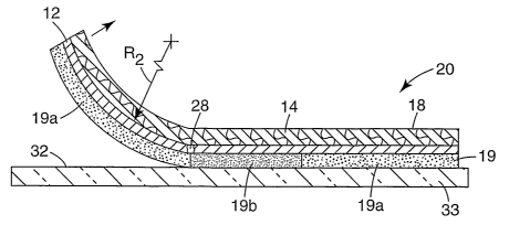
Figure 4a and 4b illustrate the ability to indicate that the RFID sticker 20
has been
tampered with, after it has been applied to a surface 32. For example, the
surface 32 may
be a surface of a glass windshield 33. By the term "tamper-indicating," as it
is used
herein, including the claims, it means to indicate that the attachment of the
RFID device
10 or RFl~ sticker 20 to a surface has been interfered with, tinkered with,
altered,
modified, or adjusted after the RFID device 10 or RFID sticker 20 has been
attached to the
surface. One example of how the attachment between the RF>D sticker and the
surface
may be interfered with or how the RFID sticker 20 may be detached from the
surface 32 is
to bend or fold the densified metal powder layer 12. As illustrated in Figure
4a, the
-14-
CA 02508889 2005-06-06
WO 2004/061762 PCT/US2003/034921
densified metal powder layer 12 is bent a radius Rl. As illustrated in Figure
4b, the
densified metal powder layer 12 may be further bent to a radius R2. This
bending motion
could be replicated by wrapping the metal powder layer 12 (and with it, the
entire sticker
20) around a rod having a diameter equal to twice the distance of Rl or R2,
respectively.
Preferably, Rl is more than 25 mm. Preferably, R2 is equal to or less than 25
mm more
preferably, R2 is equal to or less than 15 mm. Most preferably, R2 is equal to
or less than
mm. With a smaller radius, the layer 12 is bent at a sharper angle or arc, as
compared
to a larger radius.
In one preferred embodiment of the RF>D sticker 20, before the densified metal
l0 powder layer 12 of the antenna is bent, the antenna responds appropriately
to a signal sent
by an interrogator. By responding appropriately, it is meant that the device
10 either back
scattus or re-radiates the sent signal, This signal may be sent before the
RF)D sticker 20 is
adhered to the surface 32 or after the RFID sticker 20 has been properly
adhered to the
surface 32. One example of an interrogator is sold by 3M Company, located in
St. Paul
MN as a Digital Library Assistant Model 701. After the tamper-indicating radio
frequency identification antenna is bent less han~or equal to a radius of 25
mm
(represented as RZ), the antenna does not respond to the signal sent by the
interrogator.
Preferably, the interrogator sends its signal from a distance greater than 15
cm from the
RFID sticker 20. If the antenna of an individual RF)D sticker 20 that is
adhered to a
surface 32 responds appropriately to an interrogator, and at some time later,
the antenna of
the same RFm sticker 20 does not respond appropriatly to an interrogator, then
this is an
indication that the RFID sticker 20 has been tampered with.
In another preferred embodiment of the RFID sticker 20, before the densified
metal
powder layer 12 of the antenna is bent, the densified metal powder layer 12 of
the antenna
includes a resistance, such as 0.01 ohms/cm for a loop antenna. After the
densified metal
powder layer 12 of the antenna is bent less than or equal to a radius of 25 mm
(R2), the
resistance of the densified metal powder layer 12 will increase, for instance
by a factor of
two. Preferably, after the densified metal powder layer 12 of the antenna is
bent equal to
or less than or equal to a radius of 25 mm, the resistance of the antenna
increases
significantly, for instant by a factor of ten or even increases infinitely. If
the densified
metal powder layer 12 of an individual RF>D sticker 20 that is adhered to a
surface 32 is
measured to have a certain resistance, and at some time later, the densified
metal powder
-15-
CA 02508889 2005-06-06
WO 2004/061762 PCT/US2003/034921
layer 12 of the same RFID sticker 20 is measured as having a higher
resistance, especially
a significantly higher resistance, then this is an indication that the RFID
sticker 20 has
been tampered with.
Conductivity and resistively are inversely related. Higher resistance in a
circuit or
densified metal layer suggests a lower conductivity and equates to the same
level of
function in a circuit or densified metal layer. Therefore, a significant
increase in
resistance usually means a significant decrease in conductivity.
In yet another preferred embodiment of the RFID sticker 20, before the
densified
metal powder layer 12 of the antenna is bent, the densified metal powder layer
12 of the
antenna includes a conductivity. After the densified metal powder layer 12 of
antenna is
bent less than or equal to a radius of 25 mm (RZ), the conductivity of the
densified metal
powder layer 12 will decrease. Preferably, after the densified metal powder
layer 12 of the
antenna is bent equal to or less than a radius of 25 mm, the conductivity of
the antenna
decreases significantly. In some instances, the conductivity decreases so much
that the
densified metal powder layer 12 of antenna becomes nonconductive. If the
densified
metal powder layer 12 of an individual RFID sticker 20,that is adhered to a
surface 32 is
measured to have a certain conductivity, and at some time later, the densified
metal
powder layer 12 of the same RFID sticker 20 is measured as having a lower
conductivity,
especially a significantly lower conductivity, then this is an indication that
the RFID
2o sticker 20 has been tampered with.
In yet another preferred embodiment of the RFID sticker 20, after the
densified
metal powder layer 12 of antenna is bent less than or equal to a radius of 25
mm (R~), a
crack or fracture 28 forms in the layer 12, as illustrated in Figure 4b. This
fracture 28
indicates that the RFID sticker 20 has been tampered with. In this fracture
area 28, a
plurality of metal particles of layer 12 mechanically separates from each
other to the point
that a disruption occurs between the particles of the layer of densified metal
powder. It is
possible that this fracture 28 will be so small that it will not be visible to
the naked eye.
Also, the fracture 28 may not be visible to the naked eye because it will be
hidden from
the viewer by the substrate 14. However, this fracture 28 will be enough to
cause: 1) the
antenna to not respond to an interrogator; 2) the resistance of the densified
metal powder
layer 12 of the antenna to increase, most likely increase significantly;
and/or 3) the
conductivity of the densified metal powder layer 12 of the antenna to
decrease, most likely
-16-
CA 02508889 2005-06-06
WO 2004/061762 PCT/US2003/034921
decrease significantly or to become nonconductive all together. If the RFID
sticker is bent
at a radius much less than 25 mm, such as 10 mm, portions of the densified
metal powder
layer 12 of the antenna will delaminate from the substrate 14.
When the metal powder was originally densified as described above, the metal
particles were sufficiently compressed together to enable the flow of
electricity through
the densified metal powder layer 12. After bending the densified metal powder
layer 12
less than or equal to a radius of 25 mm, the area of the fracture 28 becomes
un-densified
and as a result, electricity cannot flow through the metal layer 12 as it had
previously. The
metal particles of the powder layer 12 in the fracture area 28 cannot be re-
densified simply
1o by straightening the metal layer 12. 'This is why this mechanism is a good
indicator that
the RFID antenna or sticker has been tampered with.
Although it is illustrated that the adhesive layer 19 stays with the rest of
the RFID
sticker 20 as the metal layer 12 is being bent, this is not necessary.
Instead, all of the
adhesive or a portion of the adhesive layer 19 may reside on the surface 32,
as the metal
15 layer is bended. It is also useful' to have an adhesive layer 19 that
includes at least two
different portions 19a, 19b''witli~'differing adliesivelstrengths, as
described above in
reference to Figure 3a. As~the RFID sticker 20 is pulled away from the surface
32, the
second adhesive 19b with its more aggressive adhesive or stronger adhesive
strength will
require more force to continue the detachment of the RFID sticker from the
surface 32,
20 causing the RFID sticker to pull at a sharper radius, and thus, more likely
causing the
fracture 28 to occur, as described above.
It has been described above that Figures 4a-4b illustrate bending of the
densified
metal powder layer 12 at a certain radius, and thus, the rest of the RFID
sticker 20 is bent
along the same or similar radius. Another way in which to describe this motion
is to state
25 that the densified metal powder layer 12 is being folded, curled or peeled
away from the
surface 32 and thus, the rest of the RFID sticker 20 is folded, curled or
peeled away in a
similar manner.
Figure 5a illustrates an alternative RFID sticker 40 including a layer of
retroreflective material 42. The RFID sticker 40 performs in the same manner
as the
30 RFID sticker 20 described above for its tamper-indicating features. The
retroreflective
material 42 includes a first major surface 44 and a second major surface 46
opposite the
-17-
CA 02508889 2005-06-06
WO 2004/061762 PCT/US2003/034921
first major surface 44. The first layer of adhesive 19 is attached to the
second major
surface 46 of the retroreflective material layer 42. The RFm sticker 40
includes a second
layer of adhesive 52. The second layer of adhesive 52 attaches the RF)D
sticker 40 to a
surface. The second layer of adhesive 52 may include all of the
characteristics of the first
layer of adhesive 19 described above. For example, the second adhesive 52 may
include a
variety of portions including different adhesive strengths or may be stripe
coated or coated
in a pattern.
Figures 5b illustrates another alternative RFID sticker 50 including a layer
of
retroreflective material 42. The RF>D sticker 40 performs in the same manner
as the
l0 RF>D sticker 20 described above for its tamper-indicating features. The
retroreflective
layer 42 is illustrated as attached to the second major surface 18 of the
substrate 14,
opposite the densified metal layer 12, by the second layer of adhesive 52. As
mentioned
above, the second layer of adhesive 52 may include all of the characteristics
of the first
layer of adhesive 19 described above. For example, the second adhesive 52 may
include a
variety of portions including different adhesive strengths or may be stripe
coated or coated
in a pattern.
Examples of a suitable retroreflective material are disclosed in U.S. Patent
Number
4,588,258, "Cube-Corner Retroreflective Articles having Wide Angularity in
Multiple
Viewing Planes, (Hoopman), and U.S. Patent Number 5,450,235, "Flexible Cube-
Corner
2o Retroreflective Sheeting," (Smith et al.), both of which are hereby
incorporated by
reference. Other examples of suitable retroreflective materials are taught in
U.S. Pat. Nos.
3,190,178 and 2,407,680.
Figure 6a illustrates a top view of the RF)D sticker 20 (with the layer of
adhesive
removed for clarity) after the sticker 20 has been bent equal to or less than
a radius of 25
mm. As illustrated, the densified metal powder layer 12 includes several
fractures 28.
These fractures 28 are illustrated as so severe that for purposes of
illustration a gap is
shown in the densified powder material 12. The location of the fractures 28 in
row help
indicate how far the leading edge of the sticker 20 had been folded away from
the
substrate.
3o Figure 6b illustrates another embodiment of an RF>D sticker 60. The RFID
sticker
60 is the same as the RFID sticker 20 described above, except the densified
metal powder
-18-
CA 02508889 2005-06-06
WO 2004/061762 PCT/US2003/034921
layer is in the shape of a dipole antenna, instead of a loop antenna. The
fracture 28 is a
series of fractures all in a row.
In any of the embodiments of the RFID sticker described above, the RFID
sticker
may include an optional second integrated circuit 36. Preferably, this second
integrated
circuit 36 includes its own individual antenna 37. The second integrated
circuit 36 may
already be read at a distance proportional to the size of the antenna 37. It
is particularly
useful to have two integrated circuits on an RFID sticker, so that if the
first integrated
circuit 34 fails to function because its accompanying antenna 12 is folded
less than or
equal to a radius of 25 mm, then the second integrated circuit 36 can still
function, and
to thus the RFID sticker may be read by an interrogator. It is possible that
the second
integrated circuit 36 could respond to a signal from an interrogator in one
manner or could
contain one set of information, whereas the first integrated circuit 34 could
respond to a
signal from an interrogator in a different manner or could contain a second
set of
information. If the first and second integrated circuits 34, 36 of an
individual RFID sticker
60 that is adhered to a surface 32~ and both circuits 34, 36 may be read by an
interrogator,
and at some time later, the first integrated circuit 34 cannot be read by an
interrogator, but
the second integrated circuit 36 can be read by the interrogator, then this is
an indication
that the RFID sticker 60 has been tampered with.
There are several uses of the RFID antennas 10 and RFID stickers 20, 30, 40,
50,
60 described herein. For example, the RFID antennas or stickers may be applied
to a first
surface, then removed from the first surface, and tested for tampering, as
described above.
As another example, the RFID antennas or stickers may be applied to a first
surface,
removed from the first surface, applied to a second surface, and tested for
tampering, as
described above. The RFID antennas and RFID stickers are for asset
identification and
tracking and are particularly useful for providing additional protection
against fraud or
counterfeiting of those assets.
All of the RFID stickers 20, 30, 40 50 may include an optional liner for
covering
the layer of adhesive until a user is ready to adhere the sticker to a
surface.
The present invention has now been described with reference to several
embodiments thereof. The foregoing detailed description and examples have been
given
for clarity of understanding only. No unnecessary limitations are to be
understood
-19-
CA 02508889 2005-06-06
WO 2004/061762 PCT/US2003/034921
therefrom. All patents and patent applications cited herein are hereby
incorporated by
reference. It will be apparent to those skilled in the art that many changes
can be made in
the embodiments described without departing from the scope of the invention.
Thus, the
scope of the present invention should not be limited to the exact details and
structures
described herein, but rather by the structures described by the language of
the claims, and
the equivalents of those structures.
-20-