Note: Descriptions are shown in the official language in which they were submitted.
CA 02509161 2005-05-05
WO 2004/047328 PCT/EP2002/012815
-1-
TITLE
MEMORY BASED DEVICE AND METHOD FOR CHANNEL
ESTIMATION IN A DIGITAL COMMUNICATION RECEIVER
DESCRIPTION
Field of the invention
The present invention refers to telecommunication systems and in particular to
a
digital receiver for use in a CDMA (Code Division Multiple Access) system. The
invention also relates to a device and a method for the estimation of the
channel delay
profile in a digital communication receiver.
The CDMA access technique currently finds widespread use in third generation
mobile communication systems (e.g. IJMTS, CDMA2000) thanks to its higher
spectrum
efficiency with respect to other access techniques.
In a CDMA system the data sequence is spread by a pseudo noise code
(hereinafter "PN code") having a broader spectrum width. The efficiency of
these
systems is highly dependent on the capability of the receiver to continuously
maintain
precise phase synchronization between the received and the locally generated
PN code.
In fact, without a precise phase synchronization between the received and the
locally generated code, the performance loss of the receiver is in the order
of several
dB, in terms of signal to noise and interference ratio (SN1R), even for a
mismatch of
half of the chip period.
The phase synchronisation process is usually accomplished in two steps: code
acquisition and code tracking. Code acquisition is the initial search process
that brings
the phase of the locally generated code to within the chip duration (T~=1/F~)
of the
incoming code. Code tracking is the process of achieving and maintaining fine
alignment of the chip boundaries between the incoming and locally generated
codes.
In particular the present invention is concerned with the code acquisition
procedure.
A CDMA receiver is usually implemented in the form of a Rake receiver
collecting the signal energy from different multipath components and
coherently
combining their contributions. Basically, the Rake receiver consists of many
CA 02509161 2005-05-05
WO 2004/047328 PCT/EP2002/012815
-2-
independent receiving units named 'fingers', each tuned to a different replica
of the
transmitted signal. The Rake receiver works properly only if the time delays
and
amplitudes of the different mufti-path components are correctly estimated.
Within the functional modules of a Rake receiver it is therefore necessary to
consider a particular module that estimates the time delays and amplitudes of
the
different mufti-path components of the incoming signal. The detection of the
multipath
components, or briefly 'path detection', affects the capacity of CDMA systems
since
false detections or missing detections increase the transmission power
required to get
the desired Quality of Service (QoS).
Background art
In the following we describe some known methods used for the channel delay
profile estimation in CDMA receivers. These methods can be divided in two
different
groups depending on the particular architecture employed. We can consider
methods
based on the Code Delayed Architecture (CDA) or methods based on the Data
Delayed
Architecture (DDA).
In a CDA delay profile estimator one replica of the PN sequence is generated
at
the receiver and directly correlated with the received data. During the
subsequent
correlation operations the phase of the PN sequence is cyclically changed in
order to
scan other positions (i.e. delays) of the receiving search window.
In a DDA delay profile estimator the phase (i.e. delay) of the received data
is
cyclically changed whereas the phase of the PN sequence is kept fixed. The
shift of the
received data is usually obtained, by storing the received signal samples in a
delay line
and cyclically taking the samples, for the correlation operation, from the
different
positions of the delay line.
In the description of the known methods the various signals are expressed in
terms of complex envelope so that each signal is represented by the two
components:
in-phase (I) and in-quadrature (Q). The information sequence generated by the
transmitter is represented with u(n) where n is the discrete time index
related to the
information symbol period TS
u(n) = u(n ~ TS ) n = 0, 1, 2 ....
CA 02509161 2005-05-05
WO 2004/047328 PCT/EP2002/012815
-3-
The PN code sequence S(k) is expressed as
S(k)=S(k~T~)=SI(k)+j~SQ(k) k=0,1,2,...
where k is the discrete time index related to the chip period T~ . The PN
sequence is
periodic with a period of SF chips (SF is the Spreading Factor) and a
different sequence
is assigned to each user in order to minimise the cross-interference among the
users
sharing the same channel
S(k)=S(k+SF) dk >_0
The information sequence u(n) is spread by means of the multiplication of each
information symbol with the PN code sequence S(k) , made by SF subsequent
chips, as
follows
x(k)=xI(k)+j~xQ(k)=u(kdivSF)~S(k)
As a consequence the chip period T~ is SF times smaller than the symbol period
TS and, after the spreading operation, the signal bandwidth of the information
sequence
is increased by a factor SF. The discrete time index n of the information
sequence is
expressed as a function of the discrete time index k of the chip sequence by
means of
the following expression
n=kdivSF
where k div SF is the integer part of the quotient between k and SF.
The signal x(k) is then filtered and transmitted over the propagation channel.
In
the particular case of a propagation channel with only one direct path between
the
transmitter and the receiver, the base-band signal arriving at the input of
the Rake
receiver, from the receiver front-end, is denoted as y(k) and it can be
expressed as
follows
y(k) = x(k) ~ c(k) + n(k) = u(k div SF) ~ S(k) ~ c(k) + n(k)
where c(k) = cI (k) + j ~ cQ (k) represents the distortion introduced by the
propagation
channel (due to fast fading and Doppler effect) and n(k) = n, (k) + j ~ n Q
(k) represents
the effect of thermal noise plus interference.
CA 02509161 2005-05-05
WO 2004/047328 PCT/EP2002/012815
-4-
The channel delay profile is indicated with h(1) = h I (1) + j~ h a (1) where
1 is the
variable spanning over the channel delay spread. We assume that the time
spreading of
the channel is limited to H chips before the strongest received signal replica
and T chips
after that replica. As a consequence the variable 1 spans in the range
-H<-1<_T
where the value 1= 0 corresponds to the time position of the strongest signal
replica,
which is usually taken as a reference for the synchronism of the receiver.
Therefore, the
receiving search window, where the Rake receiver is able to capture the energy
of the
received multi-path components, has a length of H+T+1 chips.
Finally we define the channel delay profile energy DP(1) as follows
DP(1) = h; (1) + hQ (1)
Now we describe the following methods for the channel profile estimation:
~ Serial correlator (CDA)
~ Bank of correlators (CDA)
~ Serial correlator (DDA)
~ Matched filter (DDA)
The first method for the channel profile estimation is the serial correlator
based
on a CDA, whose structure is shown in Figure 1.
The received signal y(k) is multiplied with the complex conjugate of the PN
sequence S~ (k -1) and the result is accumulated over an integration window of
NC
subsequent chips where, for example, NC can be equal to SF. After the
integration, the
energy of the channel profile is computed by taking the squared sum of the two
signal
components. The channel profile is computed according to the following
equation
k+NC-1
h(1) _ ~ y(i) ~ S~ (i -1)
i=k
The profile energy is then given by
DP(1) _ ~ Re[h(1)] ~a + ~ Im[h(1)] ~2
CA 02509161 2005-05-05
WO 2004/047328 PCT/EP2002/012815
-5-
Each value of 1 ( - H 51 <_ T ) corresponds to one particular delay of the
code
sequence and to one point of the channel profile. The computation of one point
of the
delay profile requires a time interval of NC chips and, in general, for a
delay profile of
H+T+1 points the time required for the profile computation is equal to
t profile = (H + T + 1 ) ~ NC [chips]
In order to reduce the time required for the profile computation it is
possible to
use a bank of serial correlators where each correlator is fed with a different
replica of
the PN code sequence. For example by using H+T+1 correlators the time required
for
the profile computation reduces to NC chips as all points of the profile are
computed in
parallel.
tprofile = NC [Chips]
The block diagram of a bank of serial correlators based on the CDA solution is
shown in Figure 2. The different replicas S* (k + H), S* (k + H -1 ) . . . S*
(k -T) of the PN
code sequence are obtained by using a single code generator that writes the
code values
in a memory buffer. The different replicas of the PN code can be read,
simultaneously,
from the different positions of the memory buffer 2 as shown in Figure 3.
The serial correlator DDA represents a dual solution with respect to the
serial
correlator CDA. In the DDA solution the phase of the PN code is kept fixed
while the
phase of the received data is changed. This is obtained by storing the
received samples
in a delay line 4 and cyclically taking the samples for the correlation
operation from the
different positions of the delay line. The block diagram of the serial
correlator DDA is
shown in Figure 4.
The channel profile is computed according to the following equation
k+NC-i
h(1) _ ~ y(i + 1) ~ S* (i)
i=k
while the profile energy is given by
DP(1) _ { Re[h(1)] ~2 +~ Im[h(1)] ~2
CA 02509161 2005-05-05
WO 2004/047328 PCT/EP2002/012815
-6-
The time required for the computation of one point of the profile is the same
of
the CDA solution and it is equal to NC chips. As a consequence the time
required for
the computation of the complete profile over H+T+1 points is equal to
t profile = (H + T + 1 ) ~ NC [Chips]
By using a matched filter it is possible to reduce the time required by the
DDA
solution for the channel delay profile computation. A matched filter is a
filter whose
frequency response is designed to exactly match the frequency spectrum of the
input
signal. In CDMA systems the matched filter is tuned to match a code sequence
that is
expected to be present within the digital samples entering in the receiver.
For example,
in the case of the UMTS system, a channel suitable for the uplink channel
delay profile
estimation is the DPCCH (Dedicated Physical Control Channel).
The matched filter is the dual solution with respect to the bank of serial
correlators for the CDA. The filter is matched to the PN sequence and
therefore the
filter coefficients f~~ff (j) are obtained by means of the following
expression
f~~ff (j) = S* (NC - j ) 1 <- j <- NC
The block diagram of the matched filter is shown in Figure 5.
The matched filter detects the presence of the PN code sequence in the input
data stream; the, output of the matched filter can be viewed as a score value
indicating
the match with the code sequence. A high score value represents a good
correlation of
the input data with the PN code sequence.
The matched filter output is computed according to the following equation
k+NC-1
h(1)= ~y(i+1)~S*(i-k)
i=k
The profile energy is given by
DP(1) _ ~ Re[h(1)] ~2 +{ Im[h(1)] ~~
The time required by the matched filter to compute the channel delay profile
is equal to
the search window length, that is H+T+1 chips, plus (NC-1) chips necessary to
fill the
filter delay line with the incoming samples
CA 02509161 2005-05-05
WO 2004/047328 PCT/EP2002/012815
_7_
t profiie = H + T + 1 + (NC -1 ) [chips]
The matched filter (DDA) and the bank of correlators (CDA) offer faster path
detection
than other solutions but they present high complexity and power consumption.
The theory underlying the operations performed by a bank of correlators (CDA)
or a matched filter (DDA) for the computation of the channel delay profile in
a spread
spectrum receiver is illustrated in R. L. Pickholtz, D. L. Shilling, L. B.
Milstein,
"Theory of Spread Spectrum Communications - A Tutorial", IEEE Transactions and
Communications, Vol. COM-30, No. 5, May 1982.
The problem of reducing the complexity of the architecture of a matched filter
is
addressed in US 5,715,276. This patent relates to a matched filter (DDA), for
use as part
of a spread spectrum receiver, wherein the filter length is broken into two
halves of
length N/2 each, where N is the number of taps on the matched filter.
Although the matched filter described in US 5,715,276 requires fewer logic
gates, compared to a classical matched filter the overall hardware
implementation of the
filter is however relevant.
It is likewise well known that the architecture of a Rake receiver always
incorporates a memory buffer, for temporarily storing input data streams
(DDA), or the
locally generated PN code (CDA).
The architecture disclosed in WO 00/25437 is an example of a Rake receiver
(DDA) architecture provided with an input memory buffer, implemented as a dual-
port
RAM. The I/Q sample pairs at the input of the Rake receiver are stored in the
RAM
memory through a first port, while a second port is used for accessing the
same memory
in read mode.
Another prior art Rake receiver architecture (DDA), incorporating an input
memory buffer, is disclosed in H. Lasse, N. Jari, "A Flexible Rake receiver
Architecture
for WCDMA Mobile Terminals", Third IEEE Signal Processing Workshop on Signal
Processing Advances in Wireless Communications, Taoyuan, Taiwan, March 20-23,
2001.
Such architecture incorporates an input memory buffer, used for storing the
I/Q
sample pairs at the input of the Rake receiver, implemented as an input stream
buffer
CA 02509161 2005-05-05
WO 2004/047328 PCT/EP2002/012815
_$_
which can be comprehended as a time-sliding window divided into three parts: a
write
window allowing writing to the buffer, a pre-window and a post-window allowing
read
accesses without overlapping with the write window. The read and write
accesses are
interleaved in time in order to avoid the need of concurrent memory accesses.
A
correlator engine reads the multipath samples from the stream buffer and
performs the
despreading of the multipath components sequentially.
Another prior art Rake receiver architecture (CDA), incorporating an input
memory buffer for the different phases of the PN code sequence, is disclosed
in U.
Grob, A.L. Welti, E. Zollinger, R Kung and H. Kauffman "Microcellular Direct-
Sequence Spread-Spectrum Radio System Using N-Path RAKE Receiver", IEEE
Journal on Selected Areas in Communications, Vol. 8, June 1990.
The Applicant has tackled the problem of further reducing the overall
complexity and silicon requirement of a channel delay profile estimation unit
in a Rake
receiver.
The Applicant observes that, in a Rake receiver, a RAM buffer is always
required, independently on the choice of the receiver architecture. The RAM
buffer is
used to store the data arnving from the receiver front-end, in the case of a
DDA
architecture, or the data arriving from the Code Generator Circuit, in the
case of a CDA
architecture.
The Applicant has observed that, in the previously described technique making
use of a matched filter (DDA), the delay line of the matched filter duplicates
in part the
function of the RAM buffer for storing the data arnving from the receiver
front-end. As
a matter of fact, both the delay line and the RAM buffer store the same data.
In a similar way the Applicant has observed that, in the previously described
technique making use of a bank of correlators (CDA), the delay line, necessary
for the
generation of the different phases of the PN sequence, duplicates in part the
function of
the Rake receiver RAM buffer for storing the different PN code replicas. As a
matter of
fact, both the delay line and the RAM buffer store the same data.
In view of the above, it is an object of the invention to provide a method and
a
device for the estimation of the channel delay profile in a digital
communication
CA 02509161 2005-05-05
WO 2004/047328 PCT/EP2002/012815
-9-
receiver, allowing to reduce the hardware complexity of the Rake receiver,
reducing
consequently the silicon area of the chip on which the system is integrated.
Summary of the invention
The Applicant has found that, in a Rake receiver with a DDA architecture, the
input memory buffer, used to store the data arriving from the receiver front-
end, can be
used by a channel delay profile estimation unit as an input delay line.
According to a
first aspect of the invention, a basic correlator sequentially reads the data
from the input
memory buffer of the Rake receiver, correlates them with a re-generated user
code and
stores the result in an accumulation memory.
In a second aspect thereof, the present invention relates to a channel delay
profile estimation unit for a Rake receiver with CDA architecture. The CDA
architecture uses a memory buffer for storing the PN code values arnving from
a Code
Generator Circuit. A basic correlator sequentially reads the re-generated code
elements
from the memory buffer and correlates them with the received data, storing the
results
in an accumulation memory.
The Applicant has verified that the hardware complexity of a Rake receiver can
be remarkably reduced, in relation to prior art architectures, and that a
slightly increase
in computation time is offset by the greatly reduced complexity.
Brief description of the drawings
Fig. 1 is a block diagram of a serial correlator CDA according to the prior
art;
Fig. 2 is a block diagram of a bank of serial correlators CDA according to the
prior art;
Fig. 3 describes a single PN code generator writing the PN code samples in a
memory
buffer, according to the prior art;
Fig. 4 is a block diagram of a serial correlator for DDA according to the
prior art;
Fig. 5 is a block diagram of a matched filter correlator DDA according to the
prior art;
Fig. 6 is a block diagram of a DDA architecture Rake receiver realized
according to a
first aspect of the present invention;
Fig. 7 shows a delay profile estimation unit used in the Rake receiver of
Figure 6;
Fig. 8 shows the detailed structure of a basic correlator used in a Rake
receiver realized
according to the present invention;
CA 02509161 2005-05-05
WO 2004/047328 PCT/EP2002/012815
- 10-
Fig. 9 is a block diagram of a Rake receiver realized according to a second
aspect of the
present invention; and
Fig. 10 shows a delay profile estimation unit used in the Rake receiver of
Figure 9.
Description of preferred embodiments
The Figure 6 shows a block diagram of a digital communication receiver,
realized according to a first aspect of the present invention (DDA
architecture). A Rake
receiver 10 receives an input signal y(k) , sampled at N times the chip
frequency Fc,
from a receiver front end, not shown in figure. The input signal y(k) feeds a
Random
Access Memory 16, with size equal to the channel delay spread of H+T+1 chips,
and a
delay profile estimation unit 24.
The delay profile estimation unit 24 computes the time delays and amplitudes
of
each received multipath component and it provides, as output, a channel
profile energy
DP(1) , where 1 is the variable spanning the channel delay spread.
From a functional point of view the Rake receiver 10 is a modular device made
by a plurality of independent receiving units, named fingers 18, each tuned to
a different
replica of the transmitted signal. Each finger Fl..Fn performs the operations
of
descrambling, despreading and integration on the chips of the incoming signal.
In order
to allocate the necessary number of fingers, the delay profile estimation unit
24
regularly computes the channel delay profile. The main peaks of the delay
profile are
assigned to the rake fingers 18. Since the measured delay profile is affected
by noise,
interference and fading, a suitable module 26, usually referred to as Finger
Allocation
Unit, compensates these impairments and selects the optimal positions and
number of
assigned fingers.
The outputs of the fingers 18 are combined by means of a combiner 22, whose
output 14 can be connected to subsequent modules such as deinterleavers and
channel
decoders, not shown in Figure 6.
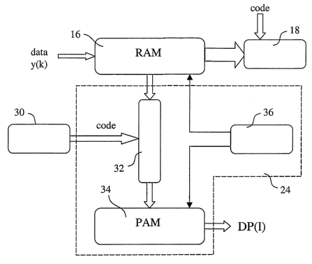
A delay profile estimation unit 24, realized according to a first aspect of
the
invention as a serial correlator DDA, is shown in detail in Figure 7. A basic
correlator
32, whose structure will be illustrated in detail in the, following with
reference to Figure
8, reads the data from .the input memory buffer (RAM) 16 of the Rake receiver
and
correlates them with the re-generated user code provided by the code generator
unit 30.
CA 02509161 2005-05-05
WO 2004/047328 PCT/EP2002/012815
-11-
The result of the correlation operation, that is the channel profile energy
DP(1), is stored
in a memory, for example a RAM memory, named Profile Accumulation Memory
(PAM) 34.
The input memory buffer (RAM) 16 and the Profile Accumulation Memory
(PAM) 34 are both addressed by a memory controller 36, so that the reading and
writing
operations of the basic correlator 32 in memories 16 and 34 are handled by the
memory
controller.
For example, the samples of the input signal y(k) can be written and read in
the
memory buffer 16 as in a circular buffer. In particular, the writing and
reading
operations can be executed through separate pointers incremented modulo the
buffer
size H+T+1.
Every NC chips, where NC is equal to the integration window size, the memory
controller 36 updates the reading pointer in the memory buffer 16 in order to
compute
the next point of the channel delay profile energy.
When the basic correlator 32 has processed the first NC chips, a first point
of the
channel profile energy DP(k) is obtained and stored into the PAM memory 34.
After
that, the basic correlator 32 changes its reading and writing position in the
memories 16
and 34 respectively and, by processing the following NC chips, it computes a
second
point DP(k + 1 ) of the channel profile energy.
A straightforward method to improve the reliability of the delay profile
estimation is to perform the non-coherent accumulation of several delay
profiles. The
non-coherent detection removes the phase rotation introduced by the channel
and allows
the sum of the energy of various delay profiles obtained at different time
instants. The
non-coherent accumulation can be expressed in formulas as follows
N
DPa~~ (1) _ ~ DP; (1) 'd 1
where Na~~ is the number of accumulations, DPa~ is the profile after non-
coherent
accumulation and DP; is the i'" channel profile energy.
In the absence of accumulations, the delay profile estimation unit 24 computes
a
delay profile of H+T+1 points, in a time equal to NCx(H+T+1) chips. If we
consider,
for instance, a delay profile of 128 points and an integration window of NC of
256, the
CA 02509161 2005-05-05
WO 2004/047328 PCT/EP2002/012815
- 12-
time required by the serial correlator for its computation is equal to 32768
chips that, for
example, correspond to about 13 slots for the FDD mode of the UMTS system.
With the
accumulation procedure necessary for improving the reliability of the
estimated delay
profile, the computation time becomes Na~ times larger. Moreover, if the
channel delay
profile is oversampled with n samples per chip, the computation time becomes n
times
larger as the number of points to be computed is nx(H+T+1) for each profile.
In order to reduce the computation time necessary for the estimation of a
delay
profile it is possible to time multiplex the basic correlator 32 at a multiple
of the chip
frequency FC. For example, with a basic correlator multiplexed at L times the
chip
frequency F~, a delay profile of H+T+1 chips, oversampled with n samples per
chip and
accumulated Na~~ times can be computed in a time equal to
NC~(H+T+1)
tprofile = N~~~ ' n ' L [chips]
On the other hand, the time multiplexing of the basic correlator increases the
access frequency to the memory buffer 16.
The architecture of the basic correlator 32 is shown in detail in the block
diagram of Figure 8. The basic correlator 32 has a first input (Data)
receiving the
complex sequence (I and Q components) of NC chips corresponding to the
received
signal y(k), and a second input (Code) receiving the complex PN code sequence
of NC
chips, generated by the code generator unit 30 shown in Figure 7.
The basic correlator 32 includes, in the particular case of a UMTS receiver
operating in FDD mode, a descrambling and despreading unit 40, for the
multiplication
between the data and the complex conjugate of the re-generated user codes, two
Integrate and Dump units 42 performing the sum of the NC partial products at
the
output of the descrambling and despreading unit, and two squaring units 44 for
computing the energy of the received symbols at the output of the Integrate
and Dump
units. The energies of the two signal components are then combined by means of
the
adder 46.
The device for the estimation of the channel delay profile previously
described
operates according to a method comprising the following steps:
CA 02509161 2005-05-05
WO 2004/047328 PCT/EP2002/012815
-13-
a) sequentially reading a first plurality of samples of the input signal y(k)
from
the memory buffer 16;
b) correlating said plurality of samples of said input signal with the re-
generated
user code for generating a first value of the channel delay profile energy
DP(k);
c) updating the reading position on the input memory buffer 16 for reading a
further plurality of samples of the input signal y(k);
d) correlating said further plurality of samples of said input signal with the
re
generated user code for generating a further value of the channel delay
profile energy
DP(k+1), the generated value of the channel delay profile energy DP(k+1) being
stored
in a profile accumulation memory 34;
e) repeating the steps c) to d) in order to compute all the points of the
channel
delay profile.
With reference to Figure 9, a digital communication receiver, realized
according
to a second aspect of the present invention, will now be described. The block
diagram of
Figure 9 illustrates a Rake receiver based on a Code Delayed Architecture
(CDA),
employing a delay profile estimation unit, or serial correlator CDA, 64, shown
in detail
in Figure 10. Since the measured delay profile is affected by noise,
interference and
fading, a suitable module 76, usually referred to as Finger Allocation Unit,
compensates
these impairments and selects the optimal positions and number of assigned
fingers.
A Rake receiver implemented with a Code Delayed Architecture (CDA) uses a
RAM memory buffer 50 to store the complex conjugate of the PN code sequence,
generated by the code generator unit 52, for a time interval equal to the
entire channel
delay spread of H+T+1 chips. The received signal y(k) is directly multiplied
in every
finger 78 with one code replica obtained through the accesses to the different
locations
of the RAM memory as shown in Figure 9. The output of the fingers 78 are
combined
by means of a combiner 72, whose output can be connected to subsequent modules
such
as interleavers and channel decoders, not shown in Figure 9. Similarly to the
DDA
architecture, the reading and writing operations in the memory buffer 50 can
be for
example organised as a circular buffer.
In the delay profile estimation unit shown in Figure 10, the re-generated user
code sequence, generated by the code generator unit 52, is stored in a RAM
memory
CA 02509161 2005-05-05
WO 2004/047328 PCT/EP2002/012815
-14-
buffer 50 of the receiver, while the received data y(k) feed directly the
basic
correlator 54.
The basic correlator 54 reads from the RAM memory buffer 50 a number of
subsequent PN code elements equal to NC and correlates them with the received
data
y(k), generating one point of the delay profile. The delay profile energy
values are
stored in the profile accumulation memory PAM 56, likewise in the DDA solution
previously illustrated.
After that, every NC chips, the basic correlator 54 updates its reading
position in
the RAM memory buffer 50 and repeats a correlation operation computing the
next
point of the channel delay profile
The addressing operations of the input memory buffer (RAM) 50 and the Profile
Accumulation Memory (PAM) 56 are handled by a memory controller 5~.
As explained above with reference to the DDA architecture, the time
multiplexing of the basic correlator 54 reduces the computation time of the
delay
profile.
The device for the estimation of the channel delay profile previously
described,
with reference to the CDA architecture, operates according to a method
comprising the
following steps:
a) sequentially reading a first plurality of samples of the re-generated user
code
from the memory buffer 50;
b) correlating said plurality of samples of said re-generated user code with
an
input signal y(k) for generating a first value of the channel delay profile
energy DP(k);
c) updating the reading position on the input memory buffer 50 for reading a
further plurality of samples of the re-generated user code;
d) correlating said further plurality of samples of said re-generated user
code
with the input signal y(k) for generating a further value of the channel delay
profile
energy DP(k+1), the generated value of the channel delay profile energy
DP(k+1) being
stored in a profile accumulation memory 56;
e) repeating the steps c) to d) in order to compute all the points of the
channel
delay profile.
CA 02509161 2005-05-05
WO 2004/047328 PCT/EP2002/012815
-15-
A delay profile estimation unit realized according to the present invention
either
implemented in a DDA architecture or in a CDA architecture rake receiver,
offers
several advantages over the prior art, in particular with respect to a matched
filter.
While the delay line of a matched filter must be implemented with a cascade of
flip-flops, the serial correlator used in the delay profile estimation unit
makes use of a
RAM memory buffer, which is already present in a rake receiver architecture.
Moreover, the serial correlator, unlike the matched filter, preserves the
receiver
modularity. In fact the serial correlator, being dedicated to a single user,
can be viewed
as a sub-system internal to the Rake receiver. Any communication burden, like
for
example the updating of the matched filter coefficients, due to the need of
sharing the
filter among several users, is avoided.