Note: Descriptions are shown in the official language in which they were submitted.
CA 02509266 2005-06-09
WO 2004/059824 PCT/IL2003/000606
Energy saving startup circuit for power supply
FIELD OF THE INVENTION
This invention relates to startup circuits for driving low voltage equipment
such as light emitting diodes (LEDs).
BACKGROUND OF THE INVENTION
Electrical equipment requiring low voltage DC are frequently energized by
mains operated power supplies. Fig. 1 shows schematically a conventional
startup
circuit 1 in a typical low voltage power supply, wherein mains voltage 2 is
rectified
typically by a bridge rectifier 3 and then fed via a resistor 4 to a control
circuit (not
shown) in the power supply. The input voltage to the control circuit is
maintained at
lo a required level by a zener diode 5 connected in parallel with a capacitor
6.
During operation, the resistor 4, which will be referred throughout as a
"starting resistor", feeds current to the capacitor 6 which therefore charges
to a
value determined by the zener diode 5, thus ensuring a constant voltage input
to the
control circuit. Typically, the mains voltage is 110 VAC in the USA or 220 VAC
in
Europe, while the equipment operates on a much lower voltage, such as 30 volts
or
even less. The startup circuit 1 serves to energize the power supply directly
from
the mains supply after it is first switched on in a controlled manner.
However, once
the power supply is operating and has reached a steady state voltage, there is
no
longer any need to supply energy to the starting circuit, which is now
redundant.
CA 02509266 2005-06-09
WO 2004/059824 PCT/IL2003/000606
-2-
A drawback with the arrangement shown in Fig. 1 is that even under steady
state conditions, when the starting circuit is no longer necessary, the
constant flow
of current through the starting resistor 4 manifests itself as a constant
energy loss,
thus reducing the overall efficiency of the power supply. The amount of power
dissipated in the starting resistor 4 is a function of the difference between
the input
voltage and the output voltage, since the closer the output voltage is to the
input
voltage in the steady state, the less is the voltage dropped across the
starting resistor
and therefore the lower is the energy loss therethrough. In power supplies
designed
to operate froin a single voltage power supply only, it is possible to
optimize the
io circuit components so as to reduce the constant energy loss through the
starting
resistor. However, in so-called universal power supplies that are intended to
operate
over a range of power supply voltages, such as 85-277 VAC so as to be suitable
for
both the US and European markets, such optimization is difficult to achieve
and it
becomes impossible to minimize the energy loss through the starting resistor
for all
supply voltages.
It would therefore be desirable to dispense with the starting resistor once
the
power supply is operating normally and reaches steady state. The prior art has
recognized this need although apparently not in a universal power supply.
Thus,
reference is made to Fig. 2 showing a prior art power supply 10 disclosed by
JP 2001275347 published Oct. 5, 2001 and assigned to Toshiba Lighting &
Technology Corporation. The reference numerals shown in the figure are those
that
are appear in the abstract of this publication, and only the relevant
components will
now be described.
The power supply unit 10 includes a starting resistor 17 that feeds the output
from a bridge rectifier 13 to a control circuit 16 on startup via a first
transistor 18. A
startup circuit feeds the output from the bridge rectifier 13 to the first
transistor 18,
thus maintaining the first transistor 18 conducting during starting and
feeding
power to the control circuit. A second transistor 21 is driven by a potential
difference between the input and the output of a voltage regulator 22 and
maintains
constant voltage generated in a priunary auxiliary winding 15b of an output
CA 02509266 2007-02-01
-3-
transformer 15 after startup. The second transistor 21 feeds the resulting
voltage to
the control circuit, which is driven thereby, and inverts the first transistor
from
conduction to cutoff thereby effectively disconnecting the starting resistor
17.
Thus, the power supply unit saves electricity during standby by separating
starting resistance after a startup (of a switching circuit), and driving the
control
circuit of a main switching element by only power generated in an output
transformer.
It will be seen from Fig. 2 that an electrolytic capacitor 23 is connected
across the input immediately after the bridge rectifier 13. The purpose of the
io electrolytic capacitor 23 is to store energy from the mains and serve as an
auxiliary
supply in the event of a momentary outage or fluctuations in the main voltage.
In
order to serve this function, the capacitor 23 must have a high capacitance
and
indeed this is the reason that an electrolytic capacitor is employed. However,
the
connection of a high capacitance at the input of the circuit militates against
the
power supply having near unity power factor. This may not matter too much when
the power supply is to be used with computers and the like. However, there are
many applications where near unity power factor is required and, in such
cases, the
circuit shown in JP 2001275347 is unsuitable.
In order to achieve near unity power factor, a high capacitance of the order
of 200 nF is usually disposed near the output of the power supply. This
increases
the time that it takes for steady state to be reached and this in turn
increases the
time before the startup circuit must be disabled. In JP 2001275347 the time
taken
between the first switch 18 opening and the second switch 14 closing is too
fast to
allow complete charging of such capacitance. This also indicates that the
circuit
disclosed in JP 2001275347 is unsuited for use with power supplies having near
unity power factor.
DE 42 27 183 discloses an electronic switching device for the delivery of a
start-up supply voltage in a switched-mode (or synchronized) power supply. A
switching device supplies the start-up supply voltage to an electronic control
circuit
whose output is connected to an electronically controlled pulse switch. After
the
CA 02509266 2007-02-01
3a-
controlled pulse switch starts pulsing, the electronically controlled circuit
is
supplied by an operating voltage circuit. A first capacitor charges when
voltage is
first applied; and a second capacitor is coupled to an output of the power
supply for
charging when a voltage appears at the output of the power supply. The first
capacitor is charged at high impedance by the input voltage. Under regular
operating conditions, and after reaching a threshold voltage, the charge of
the
second capacitor becomes available to the post-connected electronic control
circuit
at very low impedance. US 6,246,596 (Yamazaki) published June 12, 2001 and
entitled "Switching power supply" discloses a switching power supply includes
a
i o power factor improvement circuit controlled by two control ICs fed by
respective
capacitors, and at least one start-up circuit for controlling start-up of the
two control
ICs.
It would therefore be desirable to provide a startup circuit for a power
supply, particularly a universal power supply having near unity power factor,
wherein the starting resistor is disconnected after the power supply has
reached
steady state, thereby preventing energy loss and improving efficiency.
SUMMARY OF THE INVENTION
It is therefore an object of the invention to provide a startup circuit for a
power supply having near unity power factor, having a starting resistor that
is
2o disconnected after the power supply has reached steady state, thereby
preventing
energy loss and improving efficiency.
To this end there is provided in accordance with the invention a startup
circuit for a power supply, said startup circuit comprising:
an input for connecting a source of high voltage thereto,
an output rail for feeding rectified voltage to the power supply,
a first energy storage device coupled to the output rail for storing energy
when voltage is first applied to the input,
CA 02509266 2007-02-01
-4-
a second energy storage device coupled to an output of the power supply
for storing energy when a voltage appearing at the output of the power supply
reaches substantially steady state, and
a switching circuit coupled to the first energy storage device and to the
second energy storage device and being responsive to the first energy storage
device having sufficient energy for transferring said energy to the second
energy
storage device and disconnecting the first energy storage device from the
output
rail;
characterized in that:
the power supply is a universal or variable power supply that is adapted to
operate over a range of power supply voltages fed to said input,
a starting resistor is coupled between the output rail and the first energy
storage device for sourcing current to the first energy storage device, and
the switching circuit is responsive to the first energy storage device having
sufficient energy for disconnecting the starting resistor from the output
rail.
BRIEF DESCRIPTION OF THE DRAWINGS
In order to understand the invention and to see how it may be carried out in
practice, a preferred embodiment will now be described, by way of non-limiting
example only, with reference to the accompanying drawings, in which:
Fig. 1 is a partial circuit diagram showing schematically a conventional
startup circuit in a typical low voltage power supply;
Fig. 2 is a partial circuit diagram showing schematically a prior art power
supply;
Fig. 3 is a block diagram showing functionally an improved startup circuit
according to the invention; and
CA 02509266 2005-06-09
WO 2004/059824 PCT/IL2003/000606
-5-
Fig. 4 is a partial circuit diagram showing schematically a practical
embodiment of the startup circuit shown in Fig. 3.
DETAILED DESCRIPTION OF THE INVENTION
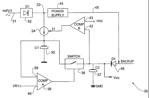
Fig. 3 is a block diagram showing functionally an improved startup circuit
30 according to the invention having an input 31 for connecting thereto a
mains
supply voltage (constituting a source of high voltage). Typically, such supply
has a
voltage of 110 VAC in the USA or 220 VAC in Europe. The input 31 is connected
to a bridge rectifier 32 having an output 33 that feeds rectified voltage to a
current
source 34 that is coupled to one end of a capacitor 35 (constituting a first
energy
lo storage device) whose other end is connected to GND.
A normally open switching circuit 36 is coupled to the first capacitor and to
a second capacitor 37 (constituting a second energy storage device) and is
responsive to the output of a first coinparator 38 having a first input 39
connected
to the positive voltage terminal of the first capacitor 35 and having a second
input
40 connected to a first reference voltage (VR1). The current source 34 is
responsively coupled to the output of a second comparator 41 having a first
input
42 connected to the positive voltage terminal of the second capacitor 37 and
having
a second input 43 connected to a second reference voltage (VR2). The rectified
output 33 of the bridge rectifier 32 is fed to a power supply 44 that is
designed to
operate near unity power factor and has an output 45 that is fed to the
cathode of a
rectifier diode 46 whose anode is connected to the positive voltage terminal
of the
second capacitor 37.
Operation of the startup circuit 30 is as follows. Upon power-up, the
constant source 34 feeds current into the first capacitor 35 and charges it to
full
charge. During this time, the rectifier output 33 feeds the power supply 44
and
charges the output capacitor (not shown) therein which ensures that the power
supply operates at or near unity power factor. The switch 36 is open, such
that the
first capacitor 35 is electrically isolated from the second capacitor 37. The
power
supply itself is not shown in Fig. 3, but once it is up and running it charges
the
CA 02509266 2005-06-09
WO 2004/059824 PCT/IL2003/000606
-6-
second capacitor 37 via the rectifier diode 46. Thus when the circuit reaches
steady
state, the second capacitor 37 serves as a reservoir to the power supply in
the event
of momentary loss of supply voltage.
When the voltage across the first capacitor 35 exceeds the first reference
voltage (VR1), the first comparator 38 produces a switching signal that causes
the
norinally open switch 36 to close, thereby connecting the first capacitor 35
in
parallel with the second capacitor 37 and transferring energy stored in first
capacitor to the second capacitor. Likewise, when the voltage across the
second
capacitor 37 exceeds the second reference voltage (VR2), the second comparator
io 41 produces a switching signal that disconnects the current source 34,
thereby
preventing further charging of the first capacitor 35. The voltage thresholds
VR1
and VR2 are chosen to be close to the voltages at full charge of the first and
second
capacitors, respectively. Thus, when the first capacitor 35 is substantially
fully
charged, the switch 36 closes and the stored energy in the first capacitor 35
is
transferred to the second capacitor 37. This helps to boost the charge on the
second
capacitor 37, which reaches the voltage threshold VR2. When this occurs, the
current source 34 is disconnected from the first capacitor 35, thus preventing
it
from becoming charged during steady state operation of the power supply and
saving energy. As will be explained below with reference to Fig. 4 of the
drawings,
the current source 34 includes a resistor via which the first capacitor 35 is
charged.
So disabling the current source 34 prevents the flow of current through this
resistor,
which would otherwise be dissipated as ohmic losses.
Referring now to Fig. 4 there will be described a partial circuit diagram
showing schematically an actual implementation of a startup circuit 40
operating as
described above with reference to Fig. 3. Features that are cominon to both
figures
will be referenced by identical reference nuinerals. Thus, the input supply
voltage
31 is fed to a bridge rectifier 32 whose positive output serves as an output
rail 33
that is fed via a first voltage divider coinprising resistors Rl and R2
connected in
series to the collector of an NPN bipolar junction transistor Q1, whose
emitter is
connected to GND. A second voltage divider is formed by a resistor R3
connected
CA 02509266 2005-06-09
WO 2004/059824 PCT/IL2003/000606
-7-
at one end to the output rail 33 and connected in series at its other end to
one end of
a resistor R4 whose other end is connected to GND.
The emitter of a PNP bipolar junction transistor Q2 is connected to the
output rail 33, its base is connected to the junction of the resistors Rl and
R2, and
its collector is connected via a resistor R5 to a first end of a first
capacitor C 1
whose second end is connected to GND and corresponds to the first capacitor 35
in
Fig. 3. The junction of the resistors R3 and R4 is connected to the collector
of an
NPN bipolar junction transistor Q3, whose emitter is connected to GND. A
resistor
R6 is connected between the base and emitter of the transistor Q3 and its base
is
io connected via a resistor R7 to the anode of a first zener diode Dl whose
cathode is
connected to a first end of a second capacitor C2 whose second end is
connected to
GND and corresponds to the second capacitor 37 in Fig. 3. The cathode of the
first
zener diode D 1 is connected to the cathode of a rectifier diode D2, whose
anode is
connected to the positive supply rail of the power supply 44.
The first end of the second capacitor C2 is also connected to the collector of
a PNP bipolar junction transistor Q4, whose emitter is connected to the first
end of
the first capacitor C 1 and whose base is connected via a resistor R8 to the
collector
of an NPN bipolar junction transistor Q5. Between the base and emitter of the
PNP
bipolar junction transistor Q4 there is connected a resistor R9. The emitter
of the
transistor Q5 is connected to GND and its base is connected to the junction of
a
voltage divider comprising series connected resistors R10 and Rll connected
between GND and the anode of a zener diode D3 whose cathode is connected to
the first end of the first capacitor C 1.
In an actual circuit reduced to practice the following circuit components
were used, where significant:
Component Value Component Value/Rating
Rl 47K C1 220
R2 100K C2 22
R3 1.5M D1 15V
R4 47K D2 -
CA 02509266 2005-06-09
WO 2004/059824 PCT/IL2003/000606
-8-
Component Value Component Value/Rating
R5 47K D3 25V
R6 10K Q1 FMMT458
R7 47K Q2 FMMT558
R8 47K Q3 PMBT222A
R9 10K Q4 PMBT2907
R10 47K Q5 BCV47
The startup circuit 40 is equivalent to the functional schematic shown in Fig.
3 and its operation is therefore identical. Thus, the PNP bipolar junction
transistor
Q2 in conjunction with the resistor R5 constitutes the current source 34 shown
in
Fig. 4. Resistors Rl, R2, R3, R4 in combination with the transistor Q 1
constitute a
first switch 50 for controlling the current source 34. Resistors R10, R11 in
combi-
nation with the zener diode D3 and the transistor Q5 constitute the first
comparator
3 8, the breakdown voltage of the zener diode D3 establishing the first
voltage
threshold VR1. Likewise, resistors R6, R7 in combination with the zener diode
D 1
io and the transistor Q3 constitute the second comparator 41, the breakdown
voltage
of the zener diode Dl establishing the first voltage threshold VR2. Resistors
R8
and R9 in combination with the transistor Q4 constitute a second switch
corresponding to the switch 36 shown in Fig. 3 for coupling the first and
second
capacitors Cl and C2. The first switch 50 and the second switch 36 may be
functionally considered as a switching circuit that is responsive to the first
capacitor
Cl having sufficient energy for transferring the energy to the second
capacitor C2
and disconnecting the first capacitor C 1.
On power-up, Q 1 is cutoff and therefore the base potential of the transistor
Q2 is substantially zero. Since Q2 is a PNP bipolar junction transistor it
conducts
current from the output rail 33 through the resistor R5, thereby charging the
first
capacitor C 1. For so long as the voltage across the first capacitor C 1 is
less than the
breakdown voltage of the zener diode D3, the base potential of the transistor
Q5 is
less than the VBE breakdown voltage and Q5, being an NPN device, is therefore
cutoff. Current flows from the current source 34 into the base of the
transistor Q4.
CA 02509266 2005-06-09
WO 2004/059824 PCT/IL2003/000606
-9-
Since Q4 is a PNP device it is therefore cutoff and the first and second
capacitors
Cl and C2 are decoupled. When the voltage across the first capacitor Cl
reaches
the breakdown voltage of the zener diode D3, the base voltage of Q5 exceeds
the
VBE breakdown voltage and transistor Q5 therefore conducts. This pulls the
base
voltage of the transistor Q4 down to GND, and Q4 being a PNP device also
starts
to conduct thereby coupling the first and second capacitors C 1 and C2,
whereby the
stored energy in C 1 flows into C2.
When the voltage across the second capacitor C2 reaches the breakdown
voltage of the zener diode Dl, the voltage across R6 exceeds the VBE breakdown
1o voltage of the transistor Q3 and Q5, being an NPN device, therefore
conducts. This
pulls the base voltage of the transistor Q 1 down to GND, and Q 1 being a NPN
device cuts off. The voltage at the base of the transistor Q2 therefore goes
high and
Q2, being a PNP device, also cuts off thereby preventing the flow of current
through the resistor R5, which would otherwise continue unnecessarily to waste
energy.
The voltage across the second capacitor C2 is now maintained by the
voltage output by the power supply 44 and the steady state operation of the
power
supply is therefore maintained without the continued operation of the startup
circuit.
It will be appreciated that the functionality of the circuit shown in Fig. 3
can
be realized using different circuit components than those shown in Fig. 4.
It will also be understood that the invention contemplates within its scope
not only the startup circuit but also a power supply containing such a startup
circuit,
being either integral therewith or connected thereto externally. Such a power
supply
has been found to be particularly efficient for use in powering light
einitting diodes
(LEDs) and may be supplied as part of an LED lighting system. Moreover, such a
power supply is amenable for connection across power supply sources of varying
voltage, such as 85-277 VAC, and is equally efficient at all voltages in the
range
since the startup circuit is disconnected as soon as the power supply reaches
steady
state. Were this not the case, the voltage dropped across the resistor R5
would
CA 02509266 2005-06-09
WO 2004/059824 PCT/IL2003/000606
-10-
depend on the voltage on the output rail 33 and more energy would be wasted at
higher supply line voltages. Thus, the drawback of variations in efficiency at
different supply line voltages is avoided.
As has been noted, it is important that such power supplies have near unity
s power factor. To this end, a high capacitance at the input of the startup
circuit as is
used in JP 2001275347 must be avoided and power factor is reduced by means of
a
suitable power factor correction circuit in the power supply, or connected to
an
output thereof. Such power factor correction circuits are known per se and are
not
themselves a feature of the invention. However, the provision of power factor
lo correction in power supplies intended for low power output, in the order of
hundreds rather than thousands of watts, militates against the connection of
high
capacitance at the input of the startup circuit and the invention therefore
embraces a
power supply having power factor correction and the startup circuit as
described.