Note: Descriptions are shown in the official language in which they were submitted.
CA 02509473 2005-06-08
03-EDP-371
-1-
METER APPARATUS AND METHOD FOR PHASE ANGLE
COMPENSATION EMPLOYING LINEAR INTERPOLATION
OF DIGITAL SIGNALS
BACKGROUND OF THE INVENTION
Field of the Invention
This invention pertains generally to meter apparatus and, more
particularly, to such apparatus receiving one or more first alternating
current
waveforms and one or more second alternating current waveforms. The invention
also pertains to a method for compensating for phase differences between first
and
second alternating current waveforms.
Background Information
In power measurement systems employing, for example, current
transformers, it is very important to correct the phase angle of related
signals (e.g.,
current and voltage signals for one or more power line phases), in order to
achieve
relatively high levels of accuracy. Previous known methods of phase angle
correction
involve analog calibration, relatively difficult digital-signal processing,
and/or
relatively high-speed sampling.
While various analog adjustments are possible, it is believed that this
analog proposal lacks the precision and consistency of digital approaches.
It is also believed that known digital-signal processing proposals are
not ideal. While a phase-shifting digital filter is possible, it is believed
that the
computation of coefficients is relatively complicated for calibration and the
real-time
requirements are relatively excessive.
Another known digital-signal processing or "digital shift" approach
requires a re-sampling process in which a number of zeros are inserted into
the digital
data stream and the high-frequency content is digitally removed with a low-
pass
digital filter. It is believed that this proposal is relatively
computationally intense and
could interfere with real-time performance.
In a relatively high-speed digital sampling approach, in order for the
sampling rate to be high enough for a suitable resolution (e.g., about 0.05
degree
resolution), at least 7200 samples/cycle are required. However, such an
approach
increases cost and complexity.
CA 02509473 2005-06-08
03-EDP-371
-2-
Accordingly, there is room for improvement in meter apparatus and
methods for compensating for phase differences between alternating current
waveforms.
SUMMARY OF THE INVENTION
These needs and others are met by the present invention, which
employs a phase angle compensation factor and adjusts sampled values of one
alternating current waveform to correspond with sampled values of another
alternating current waveform by interpolating between pairs of sampled values
of
such one alternating current waveform based upon the phase angle compensation
factor.
In accordance with one aspect of the invention, a method of
compensating for phase differences between sampled values of first and second
alternating current waveforms comprises: employing a phase angle compensation
factor; sequentially sampling a plurality of values of each of the first and
second
alternating current waveforms; and adjusting the sampled values of the second
alternating current waveform to correspond with the sampled values of the
first
alternating current waveform by employing, for a corresponding one of the
sampled
values of the second alternating current waveform, a preceding sampled value
of the
second alternating current waveform plus the product of: (i) the phase angle
compensation factor and (ii) the difference between the corresponding one of
the
sampled values and the preceding sampled value, when the phase angle
compensation
factor is positive, or alternatively adjusting the sampled values of the
second
alternating current waveform to correspond with the sampled values of the
first
alternating current waveform by employing, for the corresponding one of the
sampled
values, the preceding sampled value minus the product of: (i) the sum of one
plus the
phase angle compensation factor and (ii) the difference between the preceding
sampled value and the sampled value of the second alternating current waveform
preceding the preceding sampled value, when the phase angle compensation
factor is
negative.
The method may sequentially sample the values of each of the first and
second alternating current waveforms at a rate of about 512 samples per
alternating
CA 02509473 2005-06-08
03-EDP-371
-3-
current cycle; and employ the phase angle compensation factor, which has an
absolute
value that is smaller than one.
The method may acquire a plurality of sets of voltage samples and
current samples as sampled values of each of the first and second alternating
current
waveforms; determine a plurality of zero crossings in the voltage samples;
calculate a
plurality of zero crossing sample times for the voltage samples; determine a
plurality
of zero crossings in the current samples; calculate a plurality of zero
crossing sample
times for the current samples; calculate a plurality of differences between
the zero
crossing sample times for the voltage samples and the zero crossing sample
times for
the current samples; and average the differences to provide the phase angle
compensation factor.
The method may increment and store a count for each of the sets of
voltage samples and current samples; calculate the zero crossing sample times
for the
voltage samples by employing, for a corresponding one of the zero crossing
sample
times and a corresponding one of the voltage samples, the stored count of the
corresponding one of the voltage samples immediately before a corresponding
one of
the zero crossings plus the voltage of the voltage sample immediately before
the
corresponding one of the zero crossings divided by the difference between: (i)
the
voltage of the voltage sample immediately before the corresponding one of the
zero
crossings and (ii) the voltage of the voltage sample immediately after the
corresponding one of the zero crossings; and calculate the zero crossing
sample times
for the current samples by employing, for a corresponding one of the zero
crossing
sample times and a corresponding one of the current samples, the stored count
of the
corresponding one of the current samples immediately before a corresponding
one of
the zero crossings plus the current of the current sample immediately before
the
corresponding one of the zero crossings divided by the difference between: (i)
the
current of the current sample immediately before the corresponding one of the
zero
crossings and (ii) the current of the current sample immediately after the
corresponding one of the zero crossings.
The method may determine the count of one of the voltage zero
crossings and the current zero crossings; determine a plurality of differences
between
each of the zero crossing sample times for the voltage samples and
corresponding
CA 02509473 2005-06-08
03-EDP-371
-4-
ones of the zero crossing sample times for the current samples; sum the
differences
between each of the zero crossing sample times for the voltage samples and
corresponding ones of the zero crossing sample times for the current samples;
and
divide the sum of the differences by the count of one of the voltage zero
crossings and
the current zero crossings to determine the phase angle compensation factor.
As another aspect of the invention, a meter apparatus comprises: a
plurality of first inputs adapted to receive at least one first alternating
current
waveform; a plurality of second inputs adapted to receive at least one second
alternating current waveform; an analog to digital converter circuit adapted
to
sequentially sample and convert the received at least one first alternating
current
waveform to a plurality of first digital values and adapted to sequentially
sample and
convert the received at least one second alternating current waveform to a
plurality of
second digital values; a processor adapted to receive and process the first
and second
digital values from the analog to digital converter circuit, the processor
including a
compensation routine having a phase angle compensation factor, the
compensation
routine being adapted to adjust the second digital values to correspond with
the first
digital values by employing, for a corresponding one of the second digital
values, a
preceding one of the second digital values plus the product o~ (i) the phase
angle
compensation factor and (ii) the difference between the corresponding one of
the
second digital values and the preceding one of the second digital values, when
the
phase angle compensation factor is positive, or the routine being adapted to
alternatively adjust the second digital values to correspond with the first
digital values
by employing, for the corresponding one of the second digital values, the
preceding
one of the second digital values minus the product of: (i) the sum of one plus
the
phase angle compensation factor and (ii) the difference between the preceding
one of
the second digital values and the second digital value preceding the preceding
one of
the second digital values, when the phase angle compensation factor is
negative, in
order to compensate for phase differences between the first and second digital
values.
The processor may further include a calibration routine adapted to
receive and save a plurality of first and second digital calibration values
from the
analog to digital converter circuit, to communicate the saved first and second
digital
CA 02509473 2005-06-08
03-EDP-371
-5-
calibration values to an external calibration circuit, and to receive from the
external
calibration circuit the phase angle compensation factor.
The processor may further include a calibration routine adapted to
calibrate the phase angle compensation factor.
The compensation routine of the processor may be a first compensation
routine when the phase angle compensation factor is positive and a second
different
compensation routine when the phase angle compensation factor is negative.
As another aspect of the invention, a method of compensating for
phase differences between sampled values of first and second alternating
current
waveforms comprises: employing a phase angle compensation factor; sequentially
sampling a plurality of values of each of the first and second alternating
current
waveforms; and adjusting the sampled values of the second alternating current
waveform to correspond with the sampled values of the first alternating
current
waveform by interpolating between a corresponding one of the sampled values of
the
second alternating current waveform and a preceding sampled value of the
second
alternating current waveform, when the phase angle compensation factor is
positive,
or by interpolating between the preceding sampled value and a sampled value of
the
second alternating current waveform preceding the preceding sampled value,
when
the phase angle compensation factor is negative.
BRIEF DESCRIPTION OF THE DRAWINGS
A full understanding of the invention can be gained from the following
description of the preferred embodiments when read in conjunction with the
accompanying drawings in which:
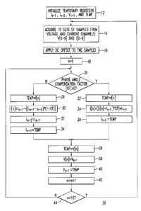
Figure 1 is a flowchart of a compensation routine for phase angle
compensation in accordance with the present invention.
Figure 2 is a flowchart of a calibration routine for calculating the phase
angle compensation factor of Figure 1.
Figure 3 is a plot of a portion of a current waveform showing application
of the phase angle compensation factor of Figure 1.
Figures 4A-4B form a flowchart of a routine for auto-calibrating a meter
in accordance with an embodiment of the invention.
CA 02509473 2005-06-08
03-EDP-371
-6-
Figures SA-SB form a flowchart of a routine for calibrating a meter with
an external calibration system in accordance with another embodiment of the
invention.
Figures 6-8 are block diagrams of meters including phase angle
compensation in accordance with other embodiments of the invention.
DESCRIPTION OF THE PREFERRED EMBODIMENTS
The present invention is described in association with meters for
determining power and/or energy from a plurality of alternating current (AC)
voltage
and current signals, although the invention is applicable to a wide range of
electrical
apparatus and methods associated with two or more AC signals.
Referring to Figure 1, a flowchart of a compensation routine 10 is shown
for phase angle compensation between sampled values of two AC waveforms. In
this
example, the phase angle compensation is applied to one of two time-varying
voltage
(V) and current (I) AC signals, although the invention is applicable to a wide
range of
signal types, to one or more phases (e.g., phase A, B and C) of current and
voltage AC
signals, and to application of phase angle compensation to the other of the
two time-
varying voltage (V) and current (I) AC signals.
First, at 12, temporary registers I~_1, I"-2, V"-~ and Temp are initialized to
zero. Next, at 14, ten sets of samples V[n] and I[n] from voltage and current
channels
(not shown), respectively, are acquired and saved for integer n ranging from 0
to 9.
Although ten sets of samples are disclosed, one to nine, eleven or more sets
of samples
may be employed. Preferably, step 14 sequentially samples the values of each
of the
voltage and current waveforms from those channels at a rate of about 512
samples per
AC cycle. Although an example sample rate is disclosed, a wide range of
suitable
smaller or larger sample rates may be employed. At 16, a predetermined direct
current
(DC) offset per channel may be applied to the samples. Preferably, this
corrects for any
known DC offset errors in the acquisition circuit (not shown) for each of the
channels.
Next, at 18, an integer, n, is set to zero. Then, at 20, it is determined if a
predetermined
phase angle compensation factor (CF) is greater than zero. If so, then steps
22, 24 and
26 are executed. Otherwise, steps 28, 30, 32 and 34 are executed. Each of
those
sequences of steps 22,24,26 and 28,30,32,34 adjusts one of the sampled values
of the
current waveform to correspond with the corresponding sampled value of the
voltage
waveform.
CA 02509473 2005-06-08
03-EDP-3 71
_7_
At 22, the first of the current samples, I [n], is saved in the temporary
register, Temp. Next, at 24, the adjusted value of the first current sample,
I[n], is
determined from Equation 1:
I[n] _ ((I[n] - I"_~) * CF) + I"_1
(Eq. 1 )
Then, at 26, the temporary register, I"_1, is set equal to the temporary
register, Temp.
Typically, the phase angle compensation factor (CF) has an absolute value that
is smaller
than one.
Otherwise, for the predetermined phase angle compensation factor (CF)
being less than zero, at 28, the first of the current samples, I[n], is saved
in the temporary
register, Temp. Next, at 30, the adjusted value of the first current sample,
I[n], is
determined from Equation 2:
I[n] = In-1 ' ((In-1 - In-2) * (1+ CF))
(Eq. 2)
Then, at 32, the temporary register, I"_2, is set equal to the temporary
register, I"_1. Next,
at 34, the temporary register, I"_I, is set equal to the temporary register,
Temp.
From Equations l and 2, it will be appreciated that no compensation is
employed if the predetermined phase angle compensation factor (CF) is zero.
At 36, the temporary register, Temp, is set equal to the first of the voltage
samples, V[n]. Next, at 38, the first voltage sample, V[n], is set equal to
the temporary
register, V~1. Then, at 40, the temporary register, Vn_l, is set equal to the
temporary
register, Temp. Next, at 42, the integer, n, is incremented. Finally, at 44,
if the integer,
n, is equal to ten, then execution resumes at 14, where a subsequent set of
ten voltage
and current samples is acquired. Otherwise, execution resumes at 20 for the
next set of
I[n] and V[n].
The routine 10 adjusts the sampled values of the current AC waveform
to correspond with the sampled values of the voltage AC waveform by
interpolating,
at 24, between a corresponding one of the sampled values of the current AC
waveform and a preceding sampled value of the current AC waveform, when the
phase angle compensation factor (CF) is positive, or by interpolating, at 30,
between
the preceding sampled value and a sampled value of the current AC waveform
CA 02509473 2005-06-08
03-EDP-371
_g_
preceding the preceding sampled value, when the phase angle compensation
factor
(CF) is negative.
In this example, with the variables being initialized to zero at step 12,
this will cause an error in the first current sample if CF is positive, or an
error in the
first and second samples if CF is negative. This error is insignificant in
meter
applications and happens only on start up or power up. Alternatively, the
first two
current samples may be ignored.
Figure 2 shows a flowchart of a calibration routine 50 for calculating the
phase angle compensation factor (CF) of Figure 1. In this example, first, at
52, 2400 sets
of digital samples are acquired from the voltage and current channels (not
shown) and
are stored in a voltage array 53 and a current array 54. Here, the actual
phase error
between a voltage channel and the corresponding current channel is determined
by
preferably inputting pure in-phase sinusoidal signals into the voltage and
current
channels. Although 2400 sets of samples is disclosed, a wide range of sample
set counts
may be employed. Next, at 55, a predetermined DC offset per channel may be
applied to
each of the samples in the arrays 53,54. Preferably, this corrects for any
known DC
offset errors in the acquisition circuit (not shown) for each of the channels.
Then, at 56,
zero crossings are determined from the values in the voltage array 53 and,
also, zero
crossing sample times are calculated and those values are stored in a voltage
time array
57. Next, at 58, zero crossings are determined from the values in the current
array 54
and, also, zero crossing sample times are calculated and those values are
stored in a
current time array 59. Then, at 60, differences between the voltage and
current crossing
sample times from the arrays 57,59 are determined and stored in a time
difference array
61. Finally, at 62, the various time differences in the array 61 are averaged,
in order to
obtain the phase angle compensation factor (CF). This phase angle compensation
factor
(CF) is stored and employed, as was discussed above in connection with Figure
1, in
order to determine how far to interpolate between the current digital samples
in the
array 54.
Figure 3 shows an example plot 70 of a portion of a current AC
waveform (I) including application of the phase angle compensation factor (CF)
of
Figure 1. This compensates for the relative phase shift of one or more current
channels (not shown) with respect to corresponding one or more voltage
channels (not
CA 02509473 2005-06-08
03-EDP-371
-9-
shown) associated with the determination of electrical power and/or energy.
The
effect of phase errors between the current and voltage channels is corrected
by
linearly interpolating a synthesized sample time between adjacent current
digital
samples, such as those at times n and n-1, or between those at times n-1 and n-
2.
In an AC power system (not shown), this is practical at rates as low as
about 64 samples/cycle and at rates as high as desired. For example, with a
specific
implementation employing 512 samples per cycle, the acquisition sub-system
(not
shown) is expected to be accurate within about a few tenths of a degree,
although one
sample time is about 0.7 degree in this example. As a result, phase correction
needs
to be much less than one sample time.
In order to correct the phase of the current waveform (I) by less than
one sample time, the compensation routine 10 of Figure 1 linearly interpolates
between adjacent digital samples. Specifically, three digital samples are
employed, in
order to provide a range of +/-1 sample time (i.e., about +/-0.7 degree at 512
samples/cycle). If the corresponding voltage waveform (not shown) is digitally
sampled at sample time "n-1 ", then the three corresponding current digital
samples
are at sample times "n", "n-1" and "n-2".
For example, as shown in Figure 3, to advance the current phase by
about 0.211 degree (i.e., 0.2109375 degree at 512 samples/cycle), use sample
times
"n-1" and "n," in order to artificially create a digital sample at sample time
"n-0.7".
In other words, linearly interpolate three tenths (i.e., CF = +0.3) of the way
between
the digital values at sample times "n-1" and "n".
As another example, to retard the current phase by about 0.07 degree
(i.e., 0.0703125 degree at 512 samples/cycle), use sample times "n-2" and "n-
1," in
order to artificially create a digital sample at sample time "n-1.1" (not
shown). In
other words, linearly interpolate a tenth of the way between the digital
values at
sample times "n-1" and "n-2".
In practice, the actual phase error is preferably measured and the result
is stored, as was discussed above in connection with Figure 2, and the stored
result is
employed in real time, as was discussed above in connection with Figure 1.
As another example, if a sampling rate of 64 samples per cycle is
employed, then the worst case error between the actual digital sample, if in
phase, and
CA 02509473 2005-06-08
03-EDP-371
-10-
the corrected digital sample is about 0.12%. This error decreases with
increases in the
sampling rate.
Figures 4A-4B show a flowchart of an auto-calibration routine 80 of a
meter (not shown). First, at 82, standard voltage and current waveforms (not
shown) are
input to the meter. For example, the standard voltage and current waveforms
(e. g. ,
without limitation, 110 VAC at 60 Hz; 10 A at 60 Hz) are preferably pure in-
phase
sinusoidal signals, which are input into the voltage and current channels (not
shown)
of the meter. Next, at 84, a command (e. g. , a suitable signal, such as, for
example, a
digital signal; a serial port signal; a data link signal; an input from a user
interface) is
input to the meter to start the auto-calibration. Then, at 86, as was
discussed above in
connection with steps 52 and 55 of Figure 2, the routine 80 acquires 2400 sets
of
current and voltage digital samples and applies DC offsets thereto.
Next, at 87, the integer, n, is set to zero. Then, at 88, the logical
expression of Equation 3 is determined to be either true or false, in order to
find a
voltage zero crossing:
(V"_1 < 0) AND (V" > 0) OR (V"_1 > 0) AND (V" < 0)
(Eq. 3 )
wherein:
V" is the voltage digital value at sample n; and
V"_1 is the preceding voltage digital value at sample n-1, except for n = 0,
wherein
V"_~ = 0.
If the test at 88 is true, then at 90, the time of the voltage zero crossing,
VoltageZeroCrossing[ ], is defined by Equation 4 with respect to the
corresponding
sample number:
VoltageZeroCrossing[ ] _ (n-1) + Vn_1~(Vn_1 - V°)
(Eq. 4)
Otherwise, or after step 90, it is determined if the integer, n, is equal to
2399. If so,
then execution resumes at step 93. Otherwise, the integer, n, is incremented
at 92
before step 88 is repeated for the next sample.
At 93, after all voltage samples are considered, the integer, n, is set to
zero. Then, at 94, the logical expression of Equation 4 is determined to be
either true
or false, in order to find a current zero crossing:
CA 02509473 2005-06-08
03-EDP-371
-11-
(I"_~ < 0) AND (I" > 0) OR (I"_1 > 0) AND (I" < 0)
(Eq. 4)
wherein:
I" is the current digital value at sample n; and
I"_1 is the preceding current digital value at sample n-1, except for n = 0,
wherein
I~_~ = 0.
If the test at 94 is true, then at 95, the time of the current zero crossing,
CurrentZeroCrossing[ ], is defined by Equation 5 with respect to the
corresponding
sample number:
CurrentZeroCrossing[ ] _ (n-1) + I"_1/(I"_1 - I")
(Eq. 5)
Otherwise, or after step 95, it is determined if the integer, n, is equal to
2399. If so,
then execution resumes at step 100. Otherwise, the integer, n, is incremented
at 98
before step 94 is repeated for the next sample.
Next, at 100, the phase angle compensation factor (CF) is determined
from Equation 6:
J
E (VoltageZeroCrossing[i] - CurrentZeroCrossing[i])
CF=1-1
ZeroCrossingCount
(Eq. 6)
wherein:
i is an integer between 1 and j; and
ZeroCrossingCount is an integer count, j, of voltage or current zero crossings
as
determined at steps 90 or 95.
Then, at 102, the meter auto-calibration routine 80 sends the
compensation factor (CF) 103 to the meter sub-system 104, which saves and
applies,
at 106, the compensation factor 103 to periodically acquired digital current
samples
(not shown).
Figures SA-SB show a flowchart of an external calibration system routine
80 for calibrating a meter 104 . The routine 80- is similar to the routine 80
of Figures
4A-4B, except that the routine 80- is executed by an external calibration
system 108,
while the auto-calibration routine 80 is internal to the meter (not shown)
associated
CA 02509473 2005-06-08
03-EDP-371
-12-
with the meter sub-system 104 of Figures 4A-4B, and except as shown by
different
reference characters in Figures SA-SB. For simplicity of disclosure, only
those
different reference characters are discussed with respect to Figures SA-SB.
At 84~ a command (e. g., a suitable signal, such as, for example, a digital
signal; a serial port signal; a data link signal) is output from the external
calibration
system 108 over a suitable port 110 (e.g., without limitation, a parallel
port; a serial port;
a data link; a communication network) to the meter 104- to start the
calibration. Then,
at 86 , as was discussed above in connection with steps 52 and 55 of Figure 2,
a meter
routine 86_ acquires 2400 sets of current and voltage digital samples and
applies DC
offsets thereto. Next, at 86 , the external calibration system 108 receives
the 2400 sets
of digital samples from the meter 104 .
At 102 , after determining the compensation factor 103 , the external
calibration system 108 sends such compensation factor over the port 110 to the
meter
104 , which saves and applies, at 106 , the compensation factor 103_ to the
periodically
acquired digital current samples (not shown).
Figure 6 shows a meter 120 including a processor 122 employing a
phase angle compensation factor (CF) 124. The meter 120 further includes one
or more
first inputs 125 adapted to receive one or more first AC waveforms 126 (e.g.,
without
limitation, voltage waveforms), and one or more second inputs 127 adapted to
receive
one or more second AC waveforms 128 (e.g., without limitation, current
waveforms).
An analog to digital converter circuit (ADC) 130 is adapted to sequentially
sample
and convert received first AC waveforms 132 to a plurality of first digital
values 134
and is adapted to sequentially sample and convert received second AC waveforms
136
to a plurality of second digital values 138.
The processor 122 includes a routine 140 adapted to receive and
process the first and second digital values 134,138 from the ADC 130. In
accordance
with an important aspect of the invention, the routine 140 cooperates with a
phase
compensation routine 142 (e.g., which may be the same as or similar to the
compensation routine 10 of Figure 1) having the phase angle compensation
factor
(CF) 124, in order to compensate for phase differences between the sampled
values
134,138. As is well known, the routine 140 and/or the ADC 130 may preferably
include suitable DC offset and/or gain adjustments for the signals 134,138.
CA 02509473 2005-06-08
03-EDP-371
-13-
The processor 122 further includes a calibration routine 144 (e.g.,
which may be the same as or similar to the auto-calibration routine 80 of
Figures 4A-
4B) adapted to calibrate the phase angle compensation factor (CF) 124. The
calibration routine 144 is executed at power up or start up (e.g., reset)
and/or at any
time responsive to a suitable command 146 received from port 148.
The routine 140 may determine power and/or energy values 150 for
display on display 151 (e.g., a local or remote display).
Referring to Figure 7, another meter 120- including a processor 122-
employing the phase angle compensation factor (CF) 124 is shown. Except as
discussed, below, the meter 120- and processor 122_ are the same as the
respective
meter 120 and processor 122 of Figure 6. Here, instead of the phase
compensation
routine 142 of Figure 6, the processor 122_ includes one or both of a first
phase
compensation routine 142- and a second different phase compensation routine
142-
The first compensation routine 142- (e.g., similar to the compensation routine
10 of
Figure 1, but excluding steps 28,30,32,34) is employed when the phase angle
compensation factor 124 is positive and the second different compensation
routine
142_ (e.g., similar to the compensation routine 10 of Figure l, but excluding
steps
22,24,26) is employed when the phase angle compensation factor 124 is
negative.
Figure 8 shows another meter 160 including processors 162 and 170
employing a phase angle compensation factor (CF) 164. The meter 160 is adapted
to
cooperate with an external calibration system, such as the system 108 of
Figures SA.
The processor 162 includes an acquisition routine 166 adapted to receive and
save a
plurality of first and second digital calibration values 167 from an analog to
digital
converter 168. The acquisition routine 166 is executed at power up or start up
of the
meter 160 or at any time with a proper command responsive to a command 172
from
the external calibration system 108 as received by a communication sub-system
174.
In this example, the command 172 is communicated to the processor 170 through
the
processor circuit 162.
After the values 167 are acquired, the processor 170 communicates
those through the host processor circuit 162 to the communication sub-system
174,
which outputs those values in a message 176 to the external calibration system
108 of
Figure SA. In turn, the external calibration system 108 determines an external
phase
CA 02509473 2005-06-08
03-EDP-371
-14-
angle compensation factor 178, which is received by the communication sub-
system
174. In this example, the external compensation factor 178 is communicated to
the
processor 170 through the host processor 162. The host processor 162 saves the
externally determined compensation factor 178 as the local compensation factor
(CF)
164 and sends the same to the processor 170 to compensate the signals.
The processor 170 also includes a routine 180 employing the phase
angle compensation factor (CF) 164, in order to compensate for phase
differences
between sampled values 182 and 184 from respective first and second AC
waveforms
126 and 128. The routine 180 may be the same as or similar to the routines
140,142
of Figure 6.
The communication sub-system 174 includes one or more suitable
communication ports.
The disclosed phase compensation techniques provide digital precision
for phase compensation without the hardware requirements of analog adjustment,
relatively high-speed sampling and relatively complicated processing. This
provides
digital accuracy with relatively minimal processing.
Although Figures 1 and 3 show phase compensation being applied to
the current AC signals, such compensation may alternatively be applied to
voltage AC
signals.
While for clarity of disclosure reference has been made herein to the
exemplary display 151 for displaying power and/or energy values, it will be
appreciated that such values may be stored, printed on hard copy, be computer
modified, be sent to a remote display, or be combined with other data. All
such
processing shall be deemed to fall within the terms "display" or "displaying"
as
employed herein.
While specific embodiments of the invention have been described in
detail, it will be appreciated by those skilled in the art that various
modifications and
alternatives to those details could be developed in light of the overall
teachings of the
disclosure. Accordingly, the particular arrangements disclosed are meant to be
illustrative only and not limiting as to the scope of the invention which is
to be given
the full breadth of the claims appended and any and all equivalents thereof.