Note: Descriptions are shown in the official language in which they were submitted.
CA 02509551 2005-06-06
1
DEVICE FOR TAILORING THE CHROMATIC DISPERSION OF A LIGHT SIGNAL
FIELD OF THE INVENTION
The present invention relates to the field of optical components and more
particularly
concerns a flexible and tunable multi-channel device for independently
assigning
specific dispersion values to each optical channel of a light signal.
BACKGROUND OF THE INVENTION
When transmitting a modulated optical signal in an optical fiber link, the
wavelength
dependence of the effective index of the fiber fundamental mode induces
differences
in the propagation delays experienced by the various spectral components. For
a
narrowband signal at a given wavelength, the propagation delay is called group
delay
(GD) and is typically expressed in ps. The GD is calculated with equation (1)
where
A is the wavelength, 0 is the optical phase and c is the speed of light.
- A2 do(A)
GD = 21rc d2 (1)
For example, the optical phase in (1) can be modified by an optical filter or
by
propagation through an optical fiber. The spectral variation of the GD is
called
chromatic dispersion (CD). The CD is the slope of the GD curve with respect to
wavelength and is expressed in ps/nm.
In the presence of CD, an optical signal is distorted and inter-symbol
interference can
appear at the output of a long fiber link. This problem is usually addressed
by the use
of CD compensators which introduce a CD with an opposite value (negative vs
positive) to that induced by a given optical fiber length. A standard G.652
optical fiber
has a CD value around 17 ps/nm-km. Optical networks with Wavelength Division
Multiplexing (WDM) transmit several optical channels spaced by 50 GHz, 100 GHz
or
200 GHz over a predetermined optical band. For example, the C-band covers the
CA 02509551 2005-06-06
2
wavelength range between 1530 nm and 1570 nm. One difficulty in CD
compensation
is that the CD is not constant between 1530 nm and 1570 nm and, furthermore,
this
variation depends on the fiber type. This wavelength dependence is called the
CD
slope (CDS) and is expressed in ps/nm2. Wideband multi-wavelength CD
compensators have to take this difference into account because CDS has a
critical
impact on the performance of high bit rate data link.
In optical networks, the CD can vary as a result of reconfigurations of the
network or
variations in the environment, for example temperature. Tunable CD
compensators
are therefore needed to dynamically adjust the CD compensation level over a
given
range. Furthermore, to have more adaptability, tunable CD compensators must be
able to compensate the CDS. Desired properties of a tunable CD compensator
therefore include flexibility on the setting of the mean CD value across the
whole
spectral band, called nominal value, and on the setting of the CDS. Ideally,
tunable
CD compensators should provide independent CD setting for each optical
channel.
This feature is particularly important when the channels present in the
covered
spectral band are propagated through different link lengths.
Fiber Bragg grating dispersion compensator
Fiber Bragg gratings (FBGs) consists of a refractive index modulation along
the fiber
axis, denoted z. The resulting effective index modulation is expressed by (
2).
nef(z)=nR1e(z)+En(z)sin n21z,)dz
( 2)
f Where neff is the effective index of the optical fiber, nave is the average
effective index,
An is the effective index modulation and AG(z) is the local grating period.
FBGs reflect
CA 02509551 2005-06-06
3
the incoming light which has spectral components close to the Bragg wavelength
(AB)
expressed in (3).
A. (Z) = 2naveAG \Z) (3)
Chirped FBGs (CFBGs) are FBGs in which AG varies along the fiber propagation
axis.
According to ( 3), the wavelength of the reflected signal, AB, will also vary
along the
optical fiber axis. This longitudinal AB variation introduces a propagation
delay
between the different spectral components of an incoming signal. The delay is
related
to the position along the fiber axis at which the reflection is maximized for
the
respective wavelengths. A single channel CD compensator may thus be realized
by
using a small linear variation of AG(z) as is schematically represented in
FIG. 1A
(PRIOR ART). Longer wavelengths of the reflected spectral band (AL) are
reflected
into the first part of the CFBG, which have shorter propagation delay, while
central
wavelengths (Ac) and shorter wavelengths (As) are reflected afterwards. For a
fixed
reflection bandwidth, the CD value of a CFBG is related to its chirp. FIG. 1B
(PRIOR
ART) illustrates a single channel CD compensator with a higher CD, with
smaller
chirp, than (a) for the same reflection bandwidth.
Single channel tunable CD compensators can be obtained by inducing a
longitudinal
variation of neff or AG which changes the reflection position of each
wavelength along
the CFBG. Different implementations of this technique are disclosed in U.S.
patent
no. 5,671,307 (Lauzon et al.) using a temperature gradient, in U.S. patent no.
5,964,501 (Alavie) and U.S. patent no. 6.360,042 (Long) with a strain gradient
or with
magnetostriction in U.S. patent no. 6,122,421 (Adams et al.).
Multi-wavelength FBG CD compensators can be obtained by superimposing many
CFBGs with spectral responses centered at different wavelengths spaced by 50
GHz,
100 GHz or 200 GHz (Y. Painchaud, H. Chotard, A. Mailloux, Y. Vasseur,
"Superposition of chirped fibre Bragg grating for third-order dispersion
compensation
CA 02509551 2005-06-06
4
over 32 WDM channels", Electronics Letters vol. 38, no. 24 , pp. 1572-1573
(2002)),
or by using FBGs sampled in amplitude and phase (H. Li, Y. Sheng, Y. Li, and
J. E.
Rothenberg, "Phased-Only Sampled Fiber Bragg Gratings for High-Channel-Count
Chromatic Dispersion Compensation", J. Lightwave Technol vol. 21, pp. 2074-
2083
Sept. 2003). In these devices, compensation of CDS is possible with proper
control of
the FBG characteristics. This is schematically demonstrated in FIGs. 2A and 2B
(PRIOR ART) where a three channel CD compensator is illustrated with a CD that
has an inter channel variation to compensate the CDS of an optical fiber link.
Similarly
to single CFBG, CD tunability is achieved by applying a longitudinal
perturbation
along the FBG. However, these devices do not offer independence of the average
CD
setting of each channel and therefore do not provide CDS tunability. To
overcome this
limitation, the use of a cascade of two multi-wavelength CD compensators is
disclosed in Canadian patent application no. 2,417,317 (Morin et al.).
CD compensators with distributed resonant cavities: principle of operation
Resonant cavity basis
Two parallel and highly reflective mirrors form a resonant optical cavity in
which
constructive interference occurs for specific cavity modes. The frequency
spacing
between each cavity mode is called the Free Spectral Range (FSR) and is
obtained
with (4), where c is speed of light in vacuum, d the distance between the
mirrors and
ng is the group index of the medium between the mirrors, ng nefrA,(dneftM%).
FSR = C
2ngd (4)
CA 02509551 2005-06-06
The spectral position of each cavity mode is evaluated with ( 5), where Am,
the mtt'
cavity mode, is directly related to the average of the effective refractive
index of the
medium.
2nave d
m (5)
5
FBG-based resonant cavities
Resonant cavities need at least two mirrors which are spatially separated. An
all-fiber
wideband resonant cavity can be formed by two CFBGs, with the same reflection
band, that are partially superimposed with a small longitudinal shift (d)
along the fiber
axis. In S. Doucet, R. Slavik, Sophie LaRochelle. " High-finesse large Band
Fabry-
Perot fibre filter with superimposed chirped Bragg Gratings ", Elec. Lett.,
Vol. 38, no
9, april 2002, pp. 160-160, a Fabry-Perot interferometer with two mirrors of
similar
reflectivity, was realized with superimposed CFBGs. Another type of
interferometer is
formed with one strong back mirror and other weaker mirror on the input side.
This
interferometer is an asymmetric Fabry-Perot, which is called a Gires-Tournois
etalon
(GTE). GTEs are used in reflection to modify the phase and to induce
dispersion on
an incident optical signal. Indeed, due to their strong back reflectors, GTEs
are
constant amplitude filters called all-pass filters. However, at the
wavelengths
corresponding to the cavity modes, the filter will introduce an important GD
on the
reflected signal. This GD is created by the resonance of the optical field
inside the
structure which results in a periodic GD response in the spectral band of the
mirrors.
By carefully designing the reflectivity and position of the weaker mirror,
GTEs allow
the shaping of the GD variations close to the Am. Similarly to Fabry-Perots,
GTEs are
realized by superimposed CFBGs. Due to the distributed nature of the CFBGs,
this
type of GTE is called a distributed Gires-Tournois etalon (DGTE). FIGs. 3A to
3C
(PRIOR ART) schematically illustrate the characteristics of a DGTE. In FIG.
3A, two
CA 02509551 2005-06-06
6
CFBGs with different modulation strengths are shown, photo-induced in an
optical
fiber but spatially shifted by d along the fiber axis. FIG. 3B represents the
relationship
between the position along the fiber axis and the local Bragg wavelength, or
maximum reflected spectral component of each CFBGs. FIG. 3B also illustrates
the
resonating cavity mode (Am, Am+1, Am+2) as well as wavelengths that are not
resonating
(Aam, Aam+i). In FIG. 3C, the GD response of a typical DGTE is illustrated. It
is shown
that the GD response follows a monotonous slope, induced by the chirp of the
CFBGs, on which GD delay peaks appear around wavelengths corresponding to the
resonant cavity modes.
Principle of CD compensator based on GTE cascade
The periodic GD response of DGTEs as explained above may advantageously be
used to build devices for CD compensation. In the simplest example of such a
device,
a single DGTE can act as a simple CD compensator when the channel bandwidth is
much smaller than the FSR of the DGTE element. However, this solution is not
viable
for high bit rate data transmission such as 10Gbit/s, 40Gbit/s or higher.
Another possibility is to use two GTE or DGTE components in a cascade
configuration, with the two components (a) and (b) having opposite chromatic
dispersion slope over the channel bandwidth. FIGs. 4A to 4F (PRIOR ART)
illustrate
the tunability principle. The upper graphs (FIGs. 4A to 4C) show the CD of the
individual components and of the cascade, while the lower graphs (FIGs 4D to
4F)
display their respective GD. The GD characteristic of component (a) shows a
quadratic dependence on wavelength detuning over a spectral region larger than
the
channel bandwidth, but smaller than one FSR, while component (b) covers the
channel bandwidth. Their cascade results in an almost linear GD as is
represented by
the dash-dot line which in turn corresponds to a constant CD over the channel
bandwidth. As can be seen by comparing the graphs from left to right, a shift
of the
spectral response of component (a) results in different CD setting over the
channel
CA 02509551 2005-06-06
7
bandwidth. A tunable multi-channel CD compensator can thus be realized because
the DGTE can be made with periodic spectral responses with a FSR of 50GHz,
100GHz, 200GHz or any desired channel spacing.
Actual chromatic dispersion compensators based on the GTE and DGTE cascade
principle
CD dispersion compensation was demonstrated with GTE filters, fabricated with
thin
film technology, and DGTE filters implemented with CFBGs. The latter case is
for
example shown in X. Shu, K. Sugden, P. Rhead, J. Mitchell, I. Felmeri, G.
Lloyd, K.
Byron, Z. Huang, Igor Khrushchev and I. Bennion, "Tunable Dispersion
Compensator
Based on Distributed Gires-Tournois Etalons," IEEE Photon. Technol. Lett. vol.
15,
pp. 1111-1113, Aug. 2003. Published patent application US2003/0210864 (Sugden
at
al.) also teaches of various DGTE-based devices for CD compensation. However,
the
proposed DGTE are limited in dispersion range and channel bandwidth.
In X. Shu, Karen Chisholm, and Kate Sugden, "Design and Realization of
Dispersion
Slope Compensator Using Distributed Gires-Tournois Etalons," IEEE Photon.
Technol. Lett. vol.16, pp.1092-1094, April 2004, it is clearly demonstrated
that CDS
compensation is possible when the DGTEs have different values of FSR. However,
the CDS is determined by the design and cannot be tuned, although tuning of
the
nominal CD, which affects the CD of all channels in similar way, remains
possible.
FIG. 5A (PRIOR ART) shows the CDS of different FSR mismatch while FIG. 5B
(PRIOR ART) shows the tuning of the device to different CD settings. It is
evident
from FIG. 5B that, although the nominal CD value changes, the inter-channel
CDS,
corresponding to the CD difference between the channels, remains constant.
In X. Shu, J. Mitchell, A. Gillooly, K. Chisholm, K. Sugden and I. Bennion,
"Tunable
dispersion Slope compensator using novel tailored Gires-Tournois etalons," in
Optical
Fiber Communication on CD-ROM (The Optical Society of America, Washington, DC,
CA 02509551 2010-10-18
8
2004), WK5, the CDS tunability is obtained by using DGTE with CFBGs with
tailored
reflectivity profiles along the fibers axis. This solution does not offer
independent
tunability of the CDS and of the nominal CD. Furthermore, some channels have a
limited dispersion range, as can be observed in FIG. 6 (PRIOR ART) for the
channels
with the shorter wavelengths.
In D.J. Moss, M. Lamont, S.McLaugthlin, G. Randall, P. Colbourne, S. Kiran and
C.A.
Hulse, "Tunable Dispersion and Dispersion Slope Compensators for 10Gb/s Using
All-Pass Multicavity Etalons," IEEE Photon. Technol. Lett. vol. 15, pp. 730-
732, May
2003, thin film multi-cavity GTEs allow compensation over a larger CD range.
CDS
compensation using two GTEs with different FSR has also been demonstrated with
this technology. Thin film GTEs have the same limitations as the previously
described
DGTE design and cannot allow complete inter-channel tunable CD compensator.
Despite all of the technological advancements described above, there is still
a need
for a versatile device which would allow for the channel-per-channel
compensation of
CD and CDS.
SUMMARY OF THE INVENTION
Accordingly, the present invention provides a device for tailoring the
chromatic
dispersion of a light signal having a plurality of periodically distributed
wavelength
channels.
The device includes a plurality of waveguide segments coupled together in a
cascade. The waveguides segments are respectively provided with spatially
distributed optical filters, which reflect the wavelength channels at
different regions
along the corresponding waveguide segment. Each optical filter has a
spectrally
continuous and periodic group delay response. The chromatic dispersion of each
wavelength channel is determined by the combined group delay response of the
CA 02509551 2010-10-18
9
optical filters along the regions of the waveguide segments reflecting the
wavelength
channel of the light signal.
The device further includes a spatially distributed tuning mechanism for
tuning,
independently in each of the regions of at least one of the waveguide
segments, the
group delay response of the corresponding optical filters.
The present invention provides a device incorporating a tuning technique
combined
with distributed filter structures which may advantageously be used as a
flexible CD
compensator. The tunability is preferably based on the distributed aspect of
the filters
and is obtained with the application of a perturbation of varying strength
along the
waveguide axis, for example temperature or strain profiles.
The present invention may therefore provide independent CD tuning of adjacent
communication channels in a given spectral region. It can therefore adjust the
CDS in
a monotonous or discrete fashion while providing significant CD compensation
over a
large dispersion range (for example, 500 ps/nm or 1000 ps/nm).
Other features and advantages of the present invention will be better
understood
upon reading of preferred embodiments thereof with reference to the appended
drawings.
BRIEF DESCRIPTION OF THE DRAWINGS
FIGs. 1A and 1B (PRIOR ART) are schematic illustrations of the principle of CD
compensation using a CFBG, respectively showing a case with a higher chirp and
lower CD and a case with a lower chirp and higher CD.
CA 02509551 2005-06-06
FIG. 2A (PRIOR ART) is a schematic illustration of superimposed single-channel
CFBGs with different chirp embodying a multi-wavelength CFBG-based CDS
compensator; FIG. 2B (PRIOR ART) is a graph of the GD experienced by the
respective channels of the compensator of FIG. 2A.
5
FIG. 3A (PRIOR ART) is a schematic representation of the implementation of a
distributed GTE using CFBGs in an optical fiber, FIG. 3B (PRIOR ART) is a
graph
showing the variation of the Bragg wavelength of the mirrors along the fiber
length;
and FIG. 3C (PRIOR ART) is a graph showing the GD response of the device.
FIGs. 4A to 4C (PRIOR ART) show the CD and FIGs. 4D to 4F show the GD of a
cascade of DGTE components (a) and (b); for FIGs. 4A and 4D without spectral
shift,
for FIGs. 4B and 4E with a shift of Component (a) to longer wavelengths, and
for
FIGs. 4C and 4F with a shift of Component (a) to shorter wavelengths.
FIG. 5A (PRIOR ART) shows plots of dispersion across channels for designed
dispersion slope compensators with different dispersion slope; and FIG. 5B
(PRIOR
ART) shows plots of dispersion across channels for a dispersion slope
compensator
when nominal dispersion varied.
FIG. 6 (PRIOR ART) shows the dispersion as a function of wavelength for
different
channels of a chromatic dispersion slope compensator using DGTE with CFBGs
with
tailored reflectivity profiles along the fibers axis.
FIG. 7 is a schematic view of a chromatic dispersion compensator configuration
according to a preferred embodiment of the invention.
FIGs. 8A to 8D illustrate the CD tuning for neighboring channels according to
another
embodiment of the invention; FIGs. 8A and 8B show a case where the inter-
channel
CA 02509551 2005-06-06
11
spacing is equal to the FSR, respectively without and with a spectral shift,
and FIGs.
8C and 8D show a case where the inter-channel spacing is twice the FSR,
respectively without and with a spectral shift.
FIG. 9 shows CFBGs mirror positions for a chirp of 0.344 nm/cm.
FIG. 10 shows CFBGs mirror positions for chirp of 0.425 nm/cm.
FIG. 1 1A shows a point to point temperature profile applied to a CD
compensator
according to an embodiment of the invention; FIG. 11B shows the resulting GD
of
each DGTE, FIG. 11 C shows the GD of the cascade, FIG. 11 D shows the channel
dispersion, and FIG. 11 E shows the GDR over the channels' bandwidth.
FIG. 12A shows another point to point temperature profile applied to a CD
compensator according to an embodiment of the invention; FIG. 12B shows the
resulting GD of each DGTE, FIG. 12C shows the GD of the cascade, FIG. 12D
shows
the channel dispersion, and FIG. 12E shows the GDR over the channels'
bandwidth.
FIGs. 13A and 13B respectively show the index modulation and the local period
of a
superstructured CFBG for use in an embodiment of the present invention.
FIGs. 14A and 14B respectively show the index modulation and the local period
of
another superstructured CFBG for use in an embodiment of the present
invention.
FIG. 15A shows a linear temperature profile with a positive slope applied to a
CD
compensator according to an embodiment of the invention; FIG. 15B shows the
resulting GD of the FBG cascade, FIG. 15C shows the resulting channel
dispersion,
and FIG. 15D shows the resulting GDR over the channels' bandwidth.
CA 02509551 2005-06-06
12
FIG. 16A shows a linear temperature profile with a negative slope applied to a
CD
compensator according to an embodiment of the invention; FIG. 16B shows the
resulting GD of the FBG cascade, FIG. 16C shows the resulting channel
dispersion,
and FIG. 16D shows the resulting GDR over the channels' bandwidth.
FIG. 17A shows a quadratic temperature profile with a positive curvature
applied to a
CD compensator according to an embodiment of the invention; FIG. 17B shows the
resulting GD of the FBG cascade, FIG. 17C shows the resulting channel
dispersion,
and FIG. 17D shows the resulting GDR over the channels' bandwidth.
FIG. 18A shows a quadratic temperature profile with a negative curvature
applied to a
CD compensator according to an embodiment of the invention; FIG. 18B shows the
resulting GD of the FBG cascade, FIG. 18C shows the resulting channel
dispersion,
and FIG. 18D shows the resulting GDR over the channels' bandwidth.
FIG. 19A shows the GD experimentally obtained by a device according to a
preferred
embodiment of the invention tuned using a linear temperature gradient; FIG.
19B
shows the corresponding CD, FIG. 19C shows the GDR and FIG. 19D shows the
FSR of the corresponding resonant cavities.
FIG. 20 is a schematic illustration of a device according to an embodiment of
the
invention.
FIG. 21A is a graph showing experimentally obtained results for the GD using a
segmented temperature profile defined by a serie of linear temperature
gradient with
the device of FIG. 20. FIG. 21 B shows the corresponding CD.
CA 02509551 2005-06-06
13
FIG. 22A is a graph showing the experimentally obtained CD with the device of
FIG.
20 using various temperature profiles; FIG. 22B shows the corresponding
temperature profiles.
DESCRIPTION OF PREFERRED EMBODIMENTS OF THE INVENTION
The present invention provides a device for tailoring the chromatic dispersion
of a
multi-channel light signal. By "tailoring", it is meant that the present
device
independently assigns specific dispersion values to each optical channel
covered by
its spectral response. Although, in the description below, the present
invention is
mainly applied to the compensation of CD in wavelength-division-multiplexed
optical
communication systems, it will be understood that the device of the present
invention
may be used in any context requiring precise control of the spectral band
location and
shape in multi-wavelength distributed optical devices. One such example is the
precise spectral positioning of the transmission peaks of the distributed
Fabry Perot
proposed in S. Doucet, R. Slavik, Sophie LaRochelle "High-finesse large Band
Fabry-
Perot fibre filter with superimposed chirped Bragg Gratings", Elec. Lett.,
Vol. 38, no 9,
april 2002, pp. 160-160. Since these all-fiber Fabry Perot filters are the
basis of the
multi-wavelength laser disclosed in Canadian Patent application no. 2,441,916
(Doucet et al.), the present invention can be used to control the spectral
position of
the laser wavelengths of these structures. Another example concerns the use of
the
per-channel CD compensator for application as a CD based encoder/decoder in
spectrum spread communications like frequency-encoded optical code division
multiple access.
Referring to FIG. 7, there is shown a device 30 according to a preferred
embodiment
of the invention. The device includes a first waveguide 32 and a second
waveguide
34, coupled together in a cascade. The waveguides 32 and 34 are preferably
embodied by optical fibers, but of course any appropriate light-guiding
structures
could be used such as planar or channel waveguides. These waveguides could be
CA 02509551 2010-10-18
14
fabricated in variety of host materials including silica, fluoride or
chalcogenide
glasses, semi-conductors, organic materials and polymers. The first and second
waveguides 32 and 34 need not be both of the same type. In the illustrated
embodiment, a 4-port optical circulator 36 couples the waveguides 32 and 34
together, and has an input port 38 for receiving the light signal to be
processed, a port
40 connected to the first waveguide 32, a port 42 connected to the second
waveguide
34, and an output port 44. It will be understood, however, that the optical
circulator 36
could be replaced by any optical arrangement allowing the input light signal
to
sequentially propagate through the first and second waveguides 32 and 34 such
as 3-
ports circulators or a combination of couplers and isolators.
It will be further noted that although the configuration shown in FIG. 7
implies that
both waveguides 32 and 34 are used in reflection, the present invention could
also be
embodied in a configuration in transmission. In addition, it will be
understood that
although the present description only shows two waveguides and two
corresponding
filters, the present invention could equally be embodied by any number of
waveguides
segments in a cascade, each provided with a corresponding optical filter
contributing
to the total chromatic dispersion of the device. The different waveguide
segments
could be part of different waveguides or even provided within a same
waveguide.
The first and second waveguides 32 and 34 are respectively provided with first
and
second optical filters 46 and 48. The optical filter 46 and 48 are spatially
distributed in
such a manner that they reflect the wavelength channels of the light signal at
different
regions along the corresponding waveguide 32 and 34. Each optical filter 46
and 48
has a spectrally periodic group delay response. The distributed optical
filters 46 and
48 could be DGTEs based on two or more partially superimposed CFBGs such as
explained above, or FBG superstructures which have complex amplitude
apodisation
and/or complex period profiles, and are spectrally designed to produce the
desired
group delay response. The resulting chromatic dispersion of each channel is
CA 02509551 2005-06-06
determined by the combined group delay response of the two optical filters 46
and 48
along the regions of the waveguides 32 and 34 reflecting this channel. By
using filters
with spectrally periodic group delay responses, the chromatic dispersion of a
given
channel is thus set by the spectral displacement between the group delay
periods of
5 the optical filters relative to the channel spectral position.
In the illustrated embodiments and explanations below, the operating principle
of a
device according to a preferred embodiment of the invention is discussed using
as an
example two DGTEs. However, the filter elements could be any FBG
superstructures,
10 i.e. FBG with complex amplitude and/or complex period profiles along the
waveguide
axis, provided that the element provides partially separated "resonating
cavities" for
the different channels. The reference to "resonant cavities" facilitates the
conceptualization of the device, but it will be understood that the optical
filters need
not be fabricated with this analogy in mind; what matters is the desired group
delay
15 response and spatial distribution. It will be noted that in order to obtain
the requisite
optical characteristics of the filters used in the present invention, the
obtained
structures will most likely be longer than prior art devices as explained
above, so that
the "resonated" cavities that generate the GD peaks are spatially separate.
In the preferred embodiment of the invention, the FBG filters are photo-
induced in an
optical fiber through UV exposure. It will be however understood that the
filters
according to the present invention could result from various fabrication
techniques
such as writing by photo-exposure or lithographic and etching processes.
The device 30 according to the present invention further includes a spatially
distributed tuning mechanism for independently tuning the group delay response
of
the first, the second or both optical filters 46 and 48 in each region of the
corresponding waveguide 32 or 34 corresponding to a given wavelength channel.
The
tuning mechanism is embodied by any system applying a perturbation of varying
CA 02509551 2005-06-06
16
strength along the optical propagation axis of the corresponding waveguide
which
affects its local properties, such as the optical length and grating period.
The
perturbation may be monotonous or discontinuous, depending on the desired
resulting CD profile. In the illustrated embodiment, the tuning mechanism is
embodied
by the generation of a thermal profile along the fiber axis. It is however
understood
that other than thermal, the perturbation could also result from the
application of a
strain profile, or from the application of electric or magnetic field profiles
if the
waveguide or its substrate present the appropriate response (electro-optic,
magneto-
optic, electrostrictive or magnetostrictive) or even current injection
profiles in the case
of semiconductor devices.
The present invention is therefore based on the combination of the tuning
mechanism, providing a perturbation along the propagation axis of a waveguide,
and
of a distributed filters written in one of the optical waveguide. The filters
provides
"resonant cavities" which induce dispersion at the channel wavelengths. The
cavities
of the tuned filter are distributed along the optical waveguide axis such that
they are
either partially overlapping or totally separated. The other filter may be
fixed or
tunable, or be embodied by one or more fixed or tunable elements producing the
desired group delay response.
Still referring to FIG. 7, the illustrated implementation of the device 30
according to a
preferred embodiment of the invention will be described in more detail. In
this
embodiment, the first optical filter is a DGTE (a) having two coupled-
cavities, and the
second optical filter 48 is a DGTE (b) having one cavity. The use of a coupled-
cavity
DGTEs increases the CD tuning range by offering more degrees of freedom on the
GD shaping for larger channel's bandwidth. Tuning is realized by a thermal
holder 50,
extending along the DGTE (a), which imposes a profiled temperature control
along
the fiber axis. In a variant, another thermal holder could be use on the DGTE
(b) to do
a fine-tuning on the spectral channel's center position.
CA 02509551 2005-06-06
17
The applied perturbation modifies the properties of the first waveguide 32
including
the optical lengths of the cavities and the local grating period. These
changes are
induced through thermo-optic and dilatation effects. Since the first optical
filter 46 is
distributed, each peak of the spectrally periodic GD is related to a specific
position
along the optical axis of the waveguide filter. The profiled perturbation
therefore
affects differently each period of the GD curve. The GD peaks of the tuned
first filter
46 are shifted by different amount relatively to the spectral response of the
second
filter 48. The channels' dispersion setting, induced by the spectral shift, is
thus a
function of the profiled perturbation.
With long distributed optical structure, it is possible to control
independently the
spectral position of each GD peak without affecting the neighboring peaks.
However,
when the FSR of the device is equal to the inter-channel spacing (ICS),
independent
positioning of the GD peaks is not sufficient to ensure independent CD tuning
of
neighboring channels. Indeed, each GD peak affects the dispersion of the two
adjacent channels located on its shorter and longer wavelength sides. FIGs. 8A
and
8C illustrate this situation (the monotonous GD slope is not represented in
the figure).
In FIG. 8C, it can be seen that the spectral shift of the GD peaks induced to
tune the
CD of the channel Am+2, affects the neighboring optical channels when ICS =
FSR. To
overcome this coupling effect and to obtain a truly multi-wavelength per-
channel CD
compensator, it is possible to use a distributed filter element with a FSR,
corresponding to the spectral spacing between consecutive peaks of the group
delay
response, which is half the inter-channel. This situation is depicted in FIG.
8B and 8D
where the tuning of channel Am+, is achieved without affecting the neighboring
channels. This configuration also allows larger excursion of the CD between
neighboring channels. When this excursion is smaller, the use of a distributed
filter
element with FSR equal to the channel spacing can be sufficient to provide
tuning of
the CD and CDS.
CA 02509551 2005-06-06
18
Preliminary design considerations
The tunability of the device according to the present invention is based on
the
distributed property of the optical filters. For optical filters based on
coupled-cavity
DGTEs, spatial independence of the resonant cavity modes depends on the cavity
length, related to the desired FSR, the number of cavities and the underlying
grating
chirp. A simple design approach for the DGTEs consists of considering point
mirror
equivalence for each CFBG. Although this approach neglects the penetration
depth of
the light in the CFBG, it can be used to estimate the maximum CFBG chirp,
Cmax, to
be used for a given number of cavities. We find
FSR
Cmax~N A2 (6)
c
where FSR?, is the FSR expressed in units of wavelength, Nr, is the number of
cavities
and ? is the central wavelength of the spectral band of interest. For a two-
cavity
design, with a FSR?, of 0.4 nm (FSR,=50GHz), the maximum chirp of the grating
period is equal to 0.333 nm/cm.
FIG. 9 shows the mirrors' position along the fiber and the corresponding
position of a
few resonant cavity modes (dashed lines) for a two-coupled cavity (three-
mirror)
design. FIG. 10 shows the situation when the chirp is greater than Cmax: a
spatial
overlap occurs between neighboring resonant cavities (gray rectangle) and, as
a
consequence, temperature controls located at the z=4 mm and z=7.5 mm affect
two
GD peaks simultaneously.
For a given CFBG length, L, and FSR?,, the maximum number of channels, Nch, is
related to the CFBG chirp in (7) .
CA 02509551 2005-06-06
19
Nch :5 2nave LCmax
FSR2 (7)
Compensation of high CD values and tuning over a large CD range require a
higher
number of coupled cavities, which consequently limits the grating chirp
through (6)
and, as a result, the number of channels covered by the CD compensator for a
given
length through (7).
It should be noted that although this schematic representation of DGTE is
useful as
an initial design step, the final design is accurately determined by CFBG
simulations
using transfer matrix method based on coupled modes theory (see T. Erdogan,
"Fiber
Grating Spectra," IEEE J. Lightwave Technol. vol.15, pp.1277-1294, August
1997,
where the superstructure grating is calculated by superimposition of
refractive index
modulations of the CFBGs.
Per-channel CD compensator (CD equalizer)
As explained above, the selection of a channel's CD is realized by shifting
the
spectral response of two filters placed in a cascade, i.e. by shifting the
position of the
GD peaks of the first filter with respect to those of the second filter. As
also explained,
truly independent per-channel CD compensation can be achieved by using
distributed
filter devices with FSR that are half the channel spacing. In the following
example, we
perform simulations using the DGTE specifications presented in Table 1.
Table 1 : DGTE parameters
DGTE (a) DGTE (b)
Chirp -0.25 nm/cm 0.25 nm/cm
L 95mm 95mm
An, 3.65 x10" 3.65x10"
One 1.13 x10" 0.41 x10"
Ana 0.2 0-4
di 2mm 2mm
d2 1.999975mm
CA 02509551 2005-06-06
FIGs. 11A to 11E and FIGs. 12A to 12E show the simulation results of the per-
channel CD compensator for two different temperature profiles. FIGs. 11A and
12A
show the point-to-point temperature profile along the fiber axis, while FIGs.
11 B and
5 12B show the GD of each DGTE. The GD of the cascade is displayed in FIGs.
11C
and 12C with a linear fit over the respective channel bandwidth. The slope of
this
linear fit is the dispersion, plotted in FIGs. 11 D and 12D for each channel,
while the
deviation of the GD from the linear fit is the group delay ripple (GDR) shown
in FIGs.
11 E and FIG. 12E. These results demonstrate that it is possible to introduce
flexible
10 CDS tuning over the spectral band of interest due to the independence of
the CD
setting for each channel. This device can therefore act as a dynamic
dispersion
equalizer.
Wideband CD compensator
15 When the spectral band covered by a device of a given length is increased
while
maintaining the CD tuning range, the cavities of the neighboring modes begin
to
overlap spatially. Consequently, inter-channels CD difference is limited for
these
wideband devices. However, this not a limitation when a smooth CD profile is
needed
over the spectral band covered by the filter. Moreover, the small inter-
channel CD
20 difference allows the use of filter elements with FSR corresponding to the
channel
spacing because two channels can share one GD peak of the optical filter(a)
without
constraint. The following results are based on the CD compensator architecture
proposed in FIG. 7. The optical filters are FBG superstructures with complex
amplitude and period profiles as can be seen in FIGs. 13A and 13B and FIGs.
14A
and 14B.
FIG. 15A to 15D, 16A to 16D, 17A to 17D and 18A to 18D show the results of
numerical simulations of a CD compensator according to the preferred
embodiment of
CA 02509551 2005-06-06
21
the present invention for different temperature profiles. These results
demonstrate
that the temperature profile is an inverse image of the obtained CD profile
over the
entire optical band. A modification of the mean temperature affects the
nominal CD
value, while a temperature gradient changes the CD shape over the entire
spectrum.
Experimental results
Experimental results have been obtained by the inventors and are demonstrated
in S.
Doucet, R. Slavik, S. LaRochelle, "Tunable dispersion slope compensator using
novel
Gires-Tournois Bragg grating coupled cavities," IEEE Photon. Technol. Lett.
vol. 16,
no. 11., pp. 2529-2531 Nov. 2004 for a temperature gradient profile applied on
one
element of a DGTE cascade as proposed in FIG. 7. The thermal holder is made
with
two thermoelectric elements joined by an aluminum plate on which the fiber is
placed.
FIGs. 19A to 19D show the results for 10 channels. More particularly FIG. 19B
demonstrates the CDS tunability with temperature gradients (6T/6z) of 1 C/mm.
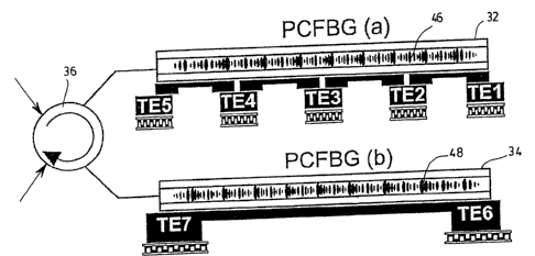
Referring to FIG. 20, there is shown a variant to the above described device
according to a preferred embodiment of the invention. In this device, the
thermal
profile tuning the first optical filter 46 is induced by creating 4 successive
temperature
gradients defined by 5 thermoelectric elements (TE1 to TE5) placed along the
fiber
holder. Thermo-electric elements are also placed on the holder of the second
optical
filter 48 to allow tuning and stabilization of the spectral position of the
channels.
In this example of the present invention the optical filters 46 and 48 are
Periodic
Complex Fiber Bragg Gratings (PCFBG), corresponding to the designs presented
in
FIGs. 13A and 13B and FIGs. 14A and 14B, were realized by using complex phase
masks. FIGs. 21A and 21B show experimental results of the CD compensator for a
CA 02509551 2005-06-06
22
quasi-quadratic CD profile. The applied temperature values were TE1=32 C;
TE2=25 C; TE3=23 C; TE4=26 C; TE5=30 C; TE6=12 C and TE7=12 C. FIGs. 22A
and 22B illustrate the CD profiles obtained with different temperature
profiles.
Of course, numerous modifications could be made to the embodiments above
without
departing from the scope of the present invention as defined in the appended
claims.