Note: Descriptions are shown in the official language in which they were submitted.
CA 02509617 2005-06-10
- 1 -
DESCRIPTION
COMMUNICATION SYSTEM, COMMUNICATION APPARATUS AND
COMMUNICATION METHOD
Technical Field
The present invention relates to a communication system,
a communication device, and a communication method, and more
particularly to, a communication system, a communication
device, and a communication method for easily solving a
problem of a so-called hidden terminal that is caused in the
wireless communication such as near field communication.
Background Art
As a near-field communication system, e.g., an IC
(Integrated Circuit) system is widely known. In the IC card
system, a reader/writer generates an electromagnetic wave,
thereby generating a so-called RF (Radio Frequency) filed
(magnetic field). An IC card is close to the reader/writer,
then, the power is supplied to the IC card received by
electromagnetic induction, and data is transferred between
the reader and the writer.
The current specification of the IC card system
includes a type A, a type B, and a type C.
The type A is used by Royal Philips Electronics as an
CA 02509617 2005-06-10
- 2 -
MIFARE system. In the type A, data is encoded by Miller in
the data transfer from the reader/writer to the IC card, and
data is encoded by Manchester in the data transfer from the
IC card to the reader and the writer. Further, the type A
uses, as a data transfer rate, 106 kbps (kilo bit per
second).
In the type B, data is encoded by NRZ in the data
transfer from the reader/writer to the IC card, and the data
is encoded by NRZ-L in the data transfer from the IC card to
the reader/writer. Further, the type B uses, as a data
transfer rate, 106 kbps.
The type C is used as a FeliCa system of Sony
Corporation serving as the present applicant. Data is
encoded by Manchester in the data transfer between the
reader and the writer and the IC card. Further, the type C
uses, as a data transfer rate, 212 kbps.
In the wireless communication such as near field
communication, the problem of the so-called hidden terminal
might be caused and therefore it is important to solve the
problem.
For example, in a conventional wireless LAN (Local Area
Network) system, generally, commands RTS (Request to send)
and CTS (Clear to send) are received and sent in the data
communication, thereby solving the problem of the hidden
terminal (e. g., in non-patent document ANSI/IEEE Std 802.11,
CA 02509617 2005-06-10
- 3 -
1999 Edition, LOCAL AND METROPOLITAN AREA NETWORKS: WIRELESS
LAN, Chapter 9 MAC sublayer functional description).
Here, the problem of the hidden terminal has the
following problems.
That is, in the wireless communication, one of a
plurality of communication devices sends data to another and
then it is controlled that both the communication devices
simultaneously do not output the electric wave
(electromagnetic wave). Specifically, the communication
device for outputting the electric wave detects the
peripheral electric wave. In the case of detecting the
peripheral electric wave, the communication device for
outputting the electric wave does not output the electric
wave. In the case of detecting no electric wave, the
communication device for outputting the electric wave
outputs the electromagnetic wave. Thus, the electric wave
is alternately outputted between the one communication
device and the other communication device for receiving and
sending data.
When the communication device for outputting the
electric wave controls the output of electric wave depending
on the presence or absence of peripheral electromagnetic
wave as mentioned above, one communication device might
simultaneously send data to other communication devices and
then the one communication device cannot receive the data.
CA 02509617 2005-06-10
- 4 -
That is, it isassumed that three communication devices
A, B, and C exist. Then, the distance between the
communication devices A and B is to control the exclusive
use of electric wave therebetween. Further, the distance
between the communication devices B and C is to control the
exclusive use of electric wave therebetween. However, the
distance between the communication devices A and C is not to
control the exclusive use of electric wave therebetween.
In this case, the communication device B does not
ZO output the electric wave when any of the communication
device A and the communication device C outputs the electric
wave. However, the communication device A outputs the
electric wave when the communication device C outputs the
electric wave. Further, the communication device C outputs
the electric wave when the communication device A outputs
the electric wave.
When the communication devices A to C have the above-
mentioned relationships, both the communication devices A
and C might simultaneously send the electric wave (data) to
the communication device B. For example, the distance
between the communication devices B and A is equal to the
distance between the communication devices B and C and both
the communication devices A and C output the electric wave
with the same strength, then, and the communication device B
receives the individual electric waves outputted from the
CA 02509617 2005-06-10
- 5 -
communication devices A and C with the same strength.
Consequently, the crosstalk does not enable the normal
reception of the data from both communication devices A and
C.
As mentioned above, the communication device B does not
normally receive the data because the communication device A
confirms the existence of the communication device B and,
however, does not confirm the existence of the communication
device C, and the communication device C further confirms
the existence of the communication device B and, however,
does not confirm the existence of the communication device A.
As mentioned above, the problem of the hidden terminal is
that both the communication devices A and C are hidden from
each other and are not viewed from each other and therefore
the crosstalk is caused in the communication device B by
simultaneously outputting the electric waves from both the
communication devices A and C.
Then, in the conventional wireless LAN, the
communication device on the communication source for
starting the communication sends the command RTS for
informing a communication time (time for sharing the space)
to the communication device serving as the communication
partner. The communication device, serving as the
communication partner, for receiving the command RTS returns
the command CTS for informing the acceptance for the command
CA 02509617 2005-06-10
- 6 -
RTS and the communication time (time for sharing the space)
to the communication device on the communication source.
Other communication devices having the distance for
receiving the command RTS or CTS from the communication
device on the communication source or as the communication
partner recognize the space sharing in one time for sharing
the space in accordance with the command RTS or CTS, and do
not send the electric wave (data) in the time for sharing
the space.
In the communication devices A to C having the above-
mentioned positional relationships, the communication device
A sends the command RTS to the communication device B, and
the communication device B sends the command CTS, serving as
a response for the command RTS, to the communication device
A. The communication device C can receive the command CTS
sent by the communication device B and the communication
device C receives the command CTS sent by the communication
device B and then does not send the electric wave.
Consequently, the communication device B prevents the
collision of electric waves (data) from the communication
devices A and C.
However, according to the solving method of the problem
of the hidden terminal by using the commands RTS and CTS,
the communication device needs control logic and memory
therefore and thus costs are increased.
CA 02509617 2005-06-10
7 _
Disclosure of Invention
The present invention is devised in consideration of
the above-mentioned situation to solve the problem of the
hidden terminal.
According to the present invention, in a communication
system, when detecting means does not detect the
electromagnetic wave at the level of a first threshold or
more, a first communication device starts to output an
electromagnetic wave and a second communication device
requires the electromagnetic wave at the level of a second
threshold or more higher than the first threshold so as to
obtain data by demodulating means.
According to the present invention, when the detecting
means does not detect the electromagnetic wave at the level
of the first threshold or more, the first communication
device starts to output the electromagnetic wave, and the
electromagnetic wave communicates with another device at the
position where it reaches at the level of the second
threshold or more higher than the first threshold.
According to the present invention, in a first
communication method, when a detecting step does not detect
the electromagnetic wave at the level of the first threshold
or more, an output of the electromagnetic wave starts and
the electromagnetic wave communicates with the other device
CA 02509617 2005-06-10
at the position where it reaches at the level of the second
threshold or more higher than the first threshold.
According to the present invention, the second
communication device requires the electromagnetic wave at
the level of the second threshold or more higher than the
first threshold so as to obtain data by demodulating means
when the other device checks that the electromagnetic wave
at the level of the first threshold or more does not exist
and the output of the electromagnetic wave starts.
According to the present invention, a second
communication method needs the electromagnetic wave at the
level of the second threshold or more higher than the first
threshold so as to obtain data by demodulating means when
the other device checks that the electromagnetic wave at the
level of the first threshold or more does not exist and the
output of the electromagnetic wave starts.
According to the present invention, in the
communication system, when the electromagnetic wave at the
level of the first threshold or more is not detected, the
first communication device starts to output the
electromagnetic wave and the second communication device
needs the electromagnetic wave at the level of the second
threshold or more higher than the first threshold so as to
obtain the data.
According to the present invention, in the first
CA 02509617 2005-06-10
- 9 -
communication device and communication method, when the
electromagnetic wave at the level of the first threshold or
more is not detected, the output of the electromagnetic wave
starts and the electromagnetic wave is communicated with the
other device at the position where it reaches at the level
of the second threshold or more higher than the first
threshold.
According to the present invention, in the second
communication device and communication method, when the
other device checks that the electromagnetic wave at the
level of the first threshold or more does not exist and the
output of the electromagnetic wave starts, the data
acquisition needs the electromagnetic wave at the level of
the second threshold or more higher than the first threshold.
Brief Description of the Drawings
Fig. 1 is a diagram showing an example of the structure
of a communication system according to a first embodiment.
Fig. 2 is an explanatory diagram of a passive mode.
Fig. 3 is an explanatory diagram of an active mode.
Fig. 4 is a block diagram showing an example of the
structure of an NFC communication device 1.
Fig. 5 is a block diagram showing one example of a
demodulating unit 13.
Fig. 6 is a block diagram showing one example of a
CA 02509617 2005-06-10
- 10 -
modulating unit
19.
Fig. 7 is a block diagram showing another example
of
the demodulating unit 13.
Fig. 8 is a block diagram showing another example
of
the demodulating unit 13.
Fig. 9 is a timing chart for explaining initial RFCA
processing.
Fig. 10 is a timing chart for explaining active RFCA
processing.
Fig. 11 is an
explanatory diagram
of SDD processing.
Fig. 12 is a diagram showing a list of commands and
responses.
Fig. 13 is a flowchart for explaining processing of
an
NFC communication
device.
Fig. 14 is a flowchart showing processing of an
initiator in the passive mode.
Fig. 15 is a flowchart showing target processing in
the
passive mode.
Fig. 16 is a flowchart showing processing of the
initiator in the active mode.
Fig. 17 is a flowchart showing target processing in
the
active mode.
Fig. 18 is a flowchart showing communication processing
of the initiator in the passive mode.
Fig. 19 is a flowchart showing communication processing
CA 02509617 2005-06-10
- 11 -
of the initiator in the passive mode.
Fig. 20 is a flowchart showing communication processing
of the target in the passive mode.
Fig. 21 is a flowchart showing communication processing
of the initiator in the active mode.
Fig. 22 is a flowchart showing communication processing
of the initiator in the active mode.
Fig. 23 is a flowchart of communication processing of
the target in the active mode.
Fig. 24 is an explanatory diagram of one example of
processing for coping with the problem of the hidden
terminal.
Fig. 25 is an explanatory diagram of another example of
processing for coping with the problem of the hidden
terminal.
Fig. 26 is an explanatory diagram of another example of
processing for coping with the problem of the hidden
terminal.
Fig. 27 is a flowchart showing processing for
controlling the reception and transmission of the initiator
in the passive mode.
Fig. 28 is a flowchart showing processing for
controlling the reception and transmission of the target in
the passive mode.
Fig. 29 is a flowchart showing processing for
CA 02509617 2005-06-10
- 12 -
controlling the reception and transmission of the initiator
in the active mode.
Fig. 30 is a flowchart showing processing for
controlling the reception and transmission of the target in
the active mode.
Best Mode for Carrying Out the Invention
Fig. 1 shows an example of the structure a
communication system (here, system is formed by logically
combining a plurality of devices, irrespective of whether or
not the devices are arranged in the same casing) according
to an embodiment.
Referring to Fig. l, the communication system comprises
three NFC communication devices l, 2, and 3. The NFC
communication devices 1 to 3 perform NFC (Near Field
Communication) by electromagnetic induction between one NFC
communication device and another with carriers having a
single frequency.
The NFC communication devices 1 to 3 use a carrier
frequency of, e.g., 13.56 MHz of ISM (Industrial Scientific
Medical) band.
The near field communication means the communication
that is established within the distance between the devices
for communication of several tens cm, including the
communication of the contact devices (casings) for
CA 02509617 2005-06-10
- 13 -
communication .
The communication system shown in Fig. 1 may be an IC
card system, in which at least one of the NFC communication
devices 1 to 3 is used as a reader/writer and further
another NFC communication device is used as an IC card. In
addition, each of the NFC communication devices 1 to 3 may
be a communication system of a PDA (Personal Digital
Assistant), a PC (Personal Computer), a mobile phone, a
watch, or a pen. That is, the NFC communication devices 1
to 3 are devices for Near-Field Communication, and are not
limited to the IC card in the IC card system or the
reader/writer.
The NFC communication devices 1 to 3 have two features.
First, the NFC communication devices 1 to 3 can communicate
data with each other in two communication modes.
Secondarily, the NFC communication devices 1 to 3 can
transfer data at a plurality of transfer rates.
The two communication modes are a passive mode and an
active mode. Now, the communication between the NFC
communication devices 1 and 2 is focused from the NFC
communication devices 1 to 3. Then, in the passive mode,
similarly to the above-mentioned conventional IC card system,
one of the NFC communication devices 1 and 2, e.g., the NFC
communication device 1 modulates (the carrier corresponding
to) the electromagnetic wave generated by the NFC
CA 02509617 2005-06-10
- 14 -
communication device l, thereby sending the data to the NFC
communication device 2 serving as the other NFC
communication device 2. The NFC communication device 2
modulates the load of (the carrier corresponding to) the
electromagnetic wave generated by the NFC communication
device l, thereby sending the data to the NFC communication
device 1.
On the other hand, in the active mode, both the NFC
communication devices 1 and 2 modulate (the carrier
corresponding to) the electromagnetic waves generated by the
NFC communication devices 1 and 2, thereby sending the data.
In the case of near field communication with the
electromagnetic induction, an initiator denotes the device
which first outputs the electromagnetic wave to start the
communication and, that is, has the initiative for
communication. In the near field communication, the
initiator sends a command to the communication partner and
the communication partner returns a response for the command,
A target denotes the communication partner that sends a
response to the command from the initiator.
For example, the NFC communication device 1 starts to
output the electromagnetic wave to start the communication
with the NFC communication device 2. Then, referring to
Figs. 2 and 3, NFC communication device 1 is the initiator,
and the NFC communication device 2 is the target.
CA 02509617 2005-06-10
- 15 -
In the passive mode, referring to Fig. 2, the NFC
communication device 1 continuously outputs the
electromagnetic wave. The NFC communication device 1
modulates the electromagnetic wave outputted by the NFC
communication device 1, thereby sending the data to the NFC
communication device 2 serving as the target. The NFC
communication device 2 modulates the load of the
electromagnetic wave outputted by the NFC communication
device 1 serving as the initiator, thereby sending the data
to the NFC communication device 1.
In the active mode, referring to Fig. 3, the NFC
communication device 1 serving as the initiator starts to
output the electromagnetic wave by itself in the case of
sending the data by itself, modulates the electromagnetic
wave, thereby sending the data to the NFC communication
device 2 serving as the target. The NFC communication
device 1 stops the output of the electromagnetic wave after
ending to send the data. The NFC communication device 2
serving as the target starts to output of the
electromagnetic wave by itself in the case of sending the
data by itself, and modulates the electromagnetic wave,
thereby sending the data to the NFC communication device 2
serving as the target. The NFC communication device 2 stops
the output of the electromagnetic wave after ending to send
the data.
CA 02509617 2005-06-10
- 16 -
The second feature that the NFC communication devices 1
to 3 can transfer the by the plurality of transfer rates
will be described later.
Referring to Fig. 1, the three NFC communication
devices 1 to 3 form the communication system. The number of
the NFC communication devices forming the communication
system is not limited to three and may be two or four or
more. Further, the communication system may include not
only the NFC communication device but also an IC card or a
reader/writer forming the conventional IC card system.
Fig. 4 shows an example of the structure of the NFC
communication device 1 shown in Fig. 1. The remaining NFC
communication devices 2 and 3 shown in Fig. 1 is similar to
the NFC communication device 1 shown in Fig. 4 and therefore
a description is omitted.
An antenna 11 forms a loop coil. The current flowing
to the coil changes and the antenna 11 outputs the
electromagnetic wave. The magnetic flux passing through the
coil serving as the antenna 11 changes, thereby flowing the
current to the antenna 11.
The receiving unit 12 receives the current flowing to
the antenna 11, tunes and detects the signal, and outputs
the signal to a demodulating unit 13. The demodulating unit
13 demodulates the signal supplied from the receiving unit
12, and supplies the demodulated signal to the decoding unit
CA 02509617 2005-06-10
- 17 -
14. The decoding unit 14 decodes Manchester code supplied
from the demodulating unit 13, and supplies data as a
decoding result to the data processing unit 15.
The data processing unit 15 performs predetermined
processing based on the data supplied from the decoding unit
14. Further, the data processing unit 15 supplies, to an
encoding unit 16, the data to be sent to another device.
The encoding unit 16 encodes the data supplied from the
data processing unit 15 to e.g., Manchester code, and
supplies the encoding data to a selecting unit 17. The
selecting unit 17 selects one of a modulating unit 19 and a
load modulation unit 20, and outputs the signal supplied
from the encoding unit 16 to the selected unit.
The selecting unit 17 selects a modulating unit 19 or a
load modulation unit 20 under the control of a control unit
21. When the communication mode is the passive mode and the
NFC communication device 1 is the target, the control unit
21 allows the selecting unit 17 to select the load
modulation unit 20. When the communication mode is the
active mode or when the communication mode is the passive
mode and the NFC communication device 1 is the initiator,
the control unit 21 allows the selecting unit 17 to select a
modulating unit 19. In the case in which the communication
mode is the passive mode and the NFC communication device 1
is the target, the signal outputted by the encoding unit 16
CA 02509617 2005-06-10
- 18 -
is supplied, via the selecting unit 17, to the load
modulation unit 20. In another case, the signal outputted
by the encoding unit 16 is supplied, via the selecting unit
17, to the modulating unit 19.
The electromagnetic-wave output unit 18 flows, from the
antenna 11 to the antenna 11, the current for irradiating
(the electromagnetic wave) of the carrier with the
predetermined single frequency. The modulating unit 19
modulates the carrier, serving as the current flowed to the
antenna 11 by the electromagnetic-wave output unit 18 in
accordance with the signal supplied from the selecting unit
17. Thus, antenna 11 irradiates the electromagnetic wave
obtained by modulating the carrier in accordance with the
data outputted to the encoding unit 16 by the processing
unit 15.
The load modulation unit 20 changes the impedance in
the case of externally viewing in accordance with the signal
supplied from the selecting unit 17. When another device
outputs the electromagnetic wave as the carrier and thus the
RF field (magnetic filed) is generated around the antenna 11,
the impedance changes in the case of externally viewing the
coil as the antenna 11, thereby changing the RF field around
the antenna 11. Consequently, the carrier serving as the
electromagnetic wave outputted by the other device is
modulated in accordance with the signal supplied from the
CA 02509617 2005-06-10
- 19 -
selecting unit 17. The data outputted from the data
processing unit 15 to the encoding unit 16 is sent to the
other device that outputs the electromagnetic wave.
The modulating system of the modulating unit 19 and the
load modulation unit 20 is e.g., ASK (Amplitude Shift
Keying). However, the modulating system of the modulating
unit 19 and the load modulation unit 20 is not limited to
ASK, and may use other modulating systems such as PSK (Phase
Shift Keying) and QAM (Quadrature Amplitude Modulation).
Further, the degree of modulation is not limited to 80, 300,
50%, and 1000 and may preferably be selected.
The control unit 21 controls the blocks forming the NFC
communication device 1. The power supply unit 22 supplies
necessary power to the blocks forming the NFC communication
device 1. Referring to Fig. 4, the drawing for controlling
the blocks forming the NFC communication device 1 by the
control unit 21 and the drawing for supplying the power to
the blocks forming the NFC communication device 1 by the
power supply unit 22 are complicated and therefore they are
omitted.
Similarly to the receiving unit 12, the detecting unit
23 receives the current flowing into the antenna 11, and
detects based on the current whether or not the antenna 11
receives the electromagnetic wave at a predetermined
threshold level (density of magnetic flux) supplied from the
CA 02509617 2005-06-10
- 20 -
threshold setting unit 24.
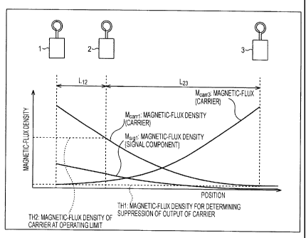
The threshold setting unit 24 sets a threshold of the
electromagnetic level detected by the detecting unit 23, and
the set threshold to the detecting unit 23. The threshold
setting unit 24 sets two thresholds (magnetic-flux density
THl for determining the suppression of output of a carrier
and a magnetic-flux density TH2 of a carrier at operating
limit, which will be described later). The detecting unit
23 detects the electromagnetic waves at a threshold level by
the threshold setting unit 24 or more from the two sets
thresholds. As shown by a dotted line in Fig. 4, the NFC
communication device 1 has the detecting unit 25 in addition
to the detecting unit 23. The detecting unit 23 detects the
electromagnetic wave having one of the two thresholds or
more. The detecting unit 25 detects the electromagnetic
wave having the other threshold or more.
In this case, the decoding unit 14 and the encoding
unit 16 process the Manchester code of the type C. The
decoding unit 14 and the encoding unit 16 selects one of a
plurality of types including modified-mirror mode in the
type A or NZR in the type C in addition to the Manchester
code, and processes the selected code.
Fig. 5 shows an example of the structure of the
demodulating unit 13 shown in Fig. 4.
Referring to Fig. 5, the demodulating unit 13
CA 02509617 2005-06-10
- 21 -
demodulates a selecting portion 31, N (>_ 2) demodulating
portions 32 i to 32N, and a selecting portion 33.
Under the control operation of the control unit 21
(shown in Fig. 4), the selecting portion 31 selects one of
the demodulating portions 32n (n = l, 2, ~~~, N) from N
demodulating portions 32 1 to 32N, and supplies a signal
outputted by the receiving unit 12 to the selected
demodulating portion 32n.
The demodulating portion 32n demodulates the signal sent
by an n-th transfer rate, and supplies the demodulated
signal to the selecting portion 33. The demodulating
portion 32n and the demodulating portion 32"~ (n ~ n')
demodulate the signals sent by different transfer rates.
Therefore, the demodulating unit 13 shown in Fig. 5
demodulates the signals sent by N (first to N-th) transfer
rates. The N transfer rates include fast 424 kbps and 848
kbps, in addition to the above-mentioned 106 kbps and 212
kbps. That is, the N transfer rates includes, e.g., the
existing transfer rates in the near field communication of
the existing IC card system and the like.
Under the control operation of the control unit 21, the
selecting portion 33 selects one demodulating portion 32n of
the N demodulating portions 32 1 to 32N, and supplies the
demodulated output obtained by the demodulating portion 32n
to the decoding unit 14.
CA 02509617 2005-06-10
- 22 -
With the demodulating unit 13 having the above
structure, the control unit 21 (shown in Fig. 4) allows the
selecting portion 31 to sequentially select N demodulating
portions 321 0 32N. Thus, the demodulating portions 321 to
S 32N demodulate the signals supplied via the selecting portion
31 from the receiving unit 12. The control unit 21
recognizes the demodulating portion 32~ that normally
demodulates the signal supplied via the selecting portion 31
from the receiving unit 12, and controls the selecting
portion 33 so as to select the output of the demodulating
portion 32n. Under the control operation of the control unit
21, the selecting portion 33 selects the demodulating
portion 32n. Thus, the output that is normally demodulated
by the demodulating portion 32n is supplied to the decoding
unit 14.
The demodulating unit 13 demodulates the signal sent by
an arbitrary transfer rate of the N transfer rates.
Only in the case of normal demodulation, the
demodulating portions 321 to 32N output a demodulating result.
In the abnormal demodulation, no data (e. g., high impedance)
is outputted. In this case, the selecting portion 33 may
sets the OR operation of all outputs of the demodulating
portions 321 to 32N and may output the OR operation to the
decoding unit 14.
Fig. 6 shows an example of the structure of the
CA 02509617 2005-06-10
- 23 -
modulating unit 19 shown in Fig. 4.
Referring to Fig. 6, the modulating unit 19 comprises a
selecting portion 41, N (>_ 2) modulating portions 421 to 42N,
and a selecting portion 43.
Under the control operation of the control unit 21 (Fig.
4), the selecting portion 41 selects one modulating portion
42~ (n = 1, 2, w , N) from N modulating portions 421 to 42N,
and supplies the signal outputted by the selecting unit 17
(Fig. 4) to the selected modulating portion 42n.
The modulating portion 42n modulates the carrier as the
current flowing into the antenna 11 via the selecting
portion 43 in accordance with the signal supplied from the
selecting portion 41 so as to send the data by the n-th
transfer rate. The modulating portion 42n and the modulating
portion 42n. (n ~ n') modulate the carrier by different
transfer rates. Referring to Fig. 6, the modulating unit 19
sends the data by N (first to N-th) transfer rates. The N
transfer rates may be the same transfer rate as that of the
demodulation of the demodulating unit 13 shown in Fig. 5.
Under the control operation of the control unit 21, the
selecting portion 43 selects the same modulating portion 42n
as that selected by the selecting portion 41 from the N
modulating portions 421 to 42N, and electrically connects the
modulating portion 42~ and the antenna 11.
For the modulating unit 19 with the above structure,
CA 02509617 2005-06-10
- 24 -
the control unit 21 (shown in Fig. 4) allows the selecting
portion 41 to sequentially select N modulating portions 421
to 42N. Thus, the control 21 further allows the modulating
portions 421 to 42N to modulate the carrier as the current
flowing into the antenna 11 via the selecting portion 43 in
accordance with the signal supplied from the selecting
portion 41.
The modulating unit 19 modulates the carrier and sends
the data so as to send the data by an arbitrary transfer
rate of the N transfer rates.
The load modulation unit 20 shown in Fig. 4 has the
same structure as that of the modulating unit 19 shown in
Fig. 6 and therefore a description thereof is omitted.
As mentioned above, the NFC communication devices 1 to
3 modulate the carrier to the signal of the data sent by any
of the N transfer rates, and further demodulate the signal
of the data sent by any of the N transfer rates. The N
transfer rate the transfer rate that has already been used
in the near field communication of the existing IC card
system (FeliCa system) and another transfer rate. Among the
NFC communication devices 1 to 3, the data is received/sent
by any of the N transfer rates. Further, among the NFC
communication devices 1 to 3, the data is received/sent
between the IC card and the reader/writer forming the
existing IC card system by the transfer rate used by the IC
CA 02509617 2005-06-10
- 25 -
card and the reader/writer.
As a consequence, the NFC communication devices 1 to 3
are easily applied to services using the existing near field
communication without user's confusion. Further, the NFC
communication devices 1 to 3 are easily applied to services
using the near field communication with the fast data rate
which will be put into the market in the future together
with the existing the near field communication.
Among the NFC communication devices 1 to 3, the data is
directly received/sent, not via another device such as a
reader/writer because the data is transferred both in the
passive mode in the conventional near field communication
and in the active mode for sending the data by outputting
the electromagnetic wave by itself.
Fig. 7 shows another example of the demodulating unit
13 shown in Fig. 4. The same reference numerals denote .the
corresponding portions in Fig. 5 and a description thereof
is properly omitted. That is, basically, the demodulating
unit 13 shown in Fig. 7 has the same structure as that Fig.
5, except for the selecting portion 31.
According to the embodiment, referring to Fig. 7, the
signal outputted by the receiving unit 12 is simultaneously
supplied to the demodulating portions 321 to 32N. The
demodulating portions 321 to 32N simultaneously demodulate
the signal from the receiving unit 12. The control unit 21
CA 02509617 2005-06-10
- 26 -
recognizes the demodulating portion 32n which normally
demodulates the signal from the receiving unit 12, and
controls the selecting portion 33 to output the signal from
the demodulating portion 32n. Under the control operation of
the control unit 21, the selecting portion 33 selects the
demodulating portion 32n, thereby supplying the output
normally demodulating the demodulating portion 32n to the
decoding unit 14.
Incidentally, according to the embodiment, referring to
Fig. 7, the demodulating portions 321 to 32N must always
demodulate the signal. On the contrary, according to the
embodiment, referring to Fig. 5, only demodulating devices
of the demodulating portions 321 to 32N that are selected by
the selecting portion 31 demodulates the signal and another
operation stops. In view of saving the power consumption of
device, the structure shown in Fig. 5 is more advantageous
than that shown in Fig. 7. On the other hand, in view of
early obtaining the normal demodulated output, the structure
shown in Fig. 7 is more advantageous than that shown in Fig.
5.
Fig. 8 shows another example of the structure of the
demodulating unit 13 shown in Fig. 4.
Referring to Fig. 8, the demodulating unit 13 comprises
a variable-rate demodulating portion 51 and a rate detecting
portion 52.
CA 02509617 2005-06-10
- 27 -
The variable-rate demodulating portion 51 demodulates
the signal supplied from the receiving unit 12 as a signal
of the transfer rate in accordance with an instruction from
the rate detecting portion 52, and supplies the demodulating
result to the decoding unit 14. The rate detecting portion
52 detects the transfer rate of the signal supplied from the
receiving unit 12 and sends an instruction for demodulating
the signal of the transfer rate to the variable-rate
demodulating portion 51.
The demodulating portion 51 with the above structure
supplies the signal outputted by the receiving unit 12 to
the variable-rate demodulating portion 51 and the rate
detecting portion 52. The rate detecting portion 52 detects
which one of the N (first to N-th) transfer rates is the
transfer rate of the signal supplied from the receiving unit
12, and sends an instruction for demodulating the signal of
the transfer rate to the variable-rate demodulating portion
51. The variable-rate demodulating portion 51 demodulates
the signal supplied from the receiving unit 12 as the signal
of the transfer rate in accordance with the instruction from
the rate detecting portion 52, and supplies the demodulating
result to the decoding unit 14.
Any of the NFC communication devices 1 to 3 can become
the initiator that first outputs the electromagnetic wave
and starts the communication. Further, in the active mode,
CA 02509617 2005-06-10
- 28 -
when any of the NFC communication devices 1 to 3 becomes the
initiator or the target, it outputs the electromagnetic wave
by itself.
When the NFC communication devices 1 to 3 are close
thereto and at least two of the NFC communication devices 1
to 3 simultaneously output the electromagnetic wave, the
collision is caused and the communication is not performed.
The NFC communication devices 1 to 3 detect whether or
not (the RF field of) the electromagnetic wave from another
device exists. Only when the RF field of the
electromagnetic wave from the other device does not exist,
the output of electromagnetic wave starts to prevent the
collision. As mentioned above, to prevent the collision,
the processing for detecting whether or not the
electromagnetic wave from another device exists and starting
the output of electromagnetic wave is referred to as RFCA
(RF Collision Avoidance) processing.
The RFCA processing includes two processing of initial
RFCA processing that is first performed by the NFC
communication device (at least one of the NFC communication
device 1 to 3 in Fig. 1) serving as the initiator and
response RFCA processing that is performed by the NFC
communication device for starting the output of
electromagnetic wave at each timing for starting the output
of electromagnetic wave in the communication in the active
CA 02509617 2005-06-10
- 29 -
mode. Both in the initial RFCA processing and the response
RFCA processing, similarly, it is detected whether or not
the electromagnetic wave from another device exists before
starting the output of electromagnetic wave and the output
of electromagnetic wave starts only when the electromagnetic
wave from the other device does not exist. However, the
time from the timing for detecting no existence of the
electromagnetic wave from the other device to the timing for
starting the output of the electromagnetic wave varies
between the initial RFCA processing and the response RFCA
processing.
First, the initial RFCA processing will be described
with reference to Fig. 9.
Fig. 9 shows the electromagnetic wave that starts to be
outputted by the initial RFCA. Referring to Fig. 9,
(similarly, Fig. 10 which will be described later), the
abscissa denotes the time and the ordinate denotes the level
of the electromagnetic wave outputted by the NFC
communication device.
The NFC communication device serving as the initiator
continuously detects the electromagnetic wave from another
device, starts the output of electromagnetic wave from the
other device when the electromagnetic wave from the other
device is not continuously detected for a time (TIpT + n x
TRH,), and starts Send Request of data (including a command)
CA 02509617 2005-06-10
- 30 -
after the passage of only time TIRFG from the output timing.
Here, the time Tlpz of the time (TIDT + n x T~.~,) is
referred to as an initial delay time. A frequency of the
carrier is designated by reference symbol f~ and then the
time TIDT as the initial delay time is larger than 4096/f~ and,
for example, is an integer that is not less than 0 and not
more than 3 and is generated by random numbers. The time
TRH, is referred to as an RF waiting time and, for example,
is 512/f~. The time TIRFG is referred to as an initial guard
time and, for example, is larger than 5 ms.
By using a random number n for the time (TIDT + n x TREN,)
for which the electromagnetic wave must not be detected, the
possibility for starting the output of electromagnetic wave
by a plurality of NFC communication devices at the same
timing is suppressed.
When the NFC communication device starts to output the
electromagnetic wave in the initial RFCA processing, the NFC
communication device becomes the initiator. In this case,
the active mode is set as a communication mode and then the
NFC communication device as the initiator ends the
transmission of the data thereof and thereafter stops the
output of electromagnetic wave. On the other hand, the
passive mode is set as a communication mode and then the NFC
communication device as the initiator continues to output
the electromagnetic wave starting by the initial RFCA
CA 02509617 2005-06-10
- 31 -
processing until the communication with the target
completely ends.
Fig. 10 shows the electromagnetic wave that start to be
outputted by the response RFCA.
In the active mode, the NFC communication device for
outputting the electromagnetic wave detects the
electromagnetic wave from another device. When the NFC
communication device does not detect the continuous output
of the electromagnetic wave from the other device only for
the time (TART + n x T,~.N,) , the output of electromagnetic wave
starts and Send Response of the data starts after the
passage of only the time TA~.~ from the output timing.
Here, reference symbols n and TRE.t", in the time (TART + n x
T~.W) are as the same in the initial RFCA processing shown in
Fig. 9. Reference symbol TApT in the time (TART + n x TRF.N,) is
referred to as an active delay time that is, e.g., 768/f~ or
more and 2559/f~ or less. The time TARFG is referred to as an
active guard time that is, e.g., longer than 1024/f~.
As will be obviously understood with reference to Figs.
9 and 10, in order to start the output of electromagnetic
wave by the initial RFCA processing, the electromagnetic
wave must exist for at least the initial delay time TIDT. In
order to start the output of electromagnetic wave by the
response RFCA processing, the electromagnetic wave must not
exist for at least the active delay time TART'
CA 02509617 2005-06-10
- 32 -
The initial delay time TInT is longer than 4096/f~. On
the other hand, the active delay time TAT is 768/f~ or more
and is 2559/f~ or less. Thus, when the NFC communication
device becomes the initiator, a.longer time for which the
electromagnetic wave does not exist is necessary, as
compared with the case in which the electromagnetic wave is
outputted during the communication in the active mode.
Inversely, when the NFC communication device outputs the
electromagnetic wave during the communication in the active
mode, the NFC communication device must output the
electromagnetic wave after not so long time from the timing
at which the electromagnetic wave does not exist, as
compared with the case in which the NFC communication device
becomes the initiator. This is because of the following
reasons.
That is, one NFC communication device communicates the
data in the active mode, then, another NFC communication
device outputs the electromagnetic wave by itself and sends
the data and thereafter stops the output of electromagnetic
wave. The other NFC communication device starts to output
the electromagnetic wave and sends the data. Therefore, in
the communication in the active mode, all the NFC.
communication devices might stop the output of
electromagnetic wave. When the NFC communication device
becomes the initiator, it is necessary to check whether or
CA 02509617 2005-06-10
- 33 -
not another device does not output the electromagnetic wave
around the NFC communication device which becomes the
initiator for a sufficient time so as to check that the data
is not communicated around the NFC communication device in
the active mode.
On the other hand, in the active mode, the initiator
outputs the electromagnetic wave, thereby sending the data
to the target. The initiator stops the output of
electromagnetic wave and then starts the output of
electromagnetic wave. Thus, the target sends the data to
the initiator. After that, the target stops the output of
electromagnetic wave and then the initiator starts to output
the electromagnetic wave, thereby sending the data to the
initiator. Then, similarly, the data is received/sent
between the initiator and the target.
When the NFC communication device exists serving as the
initiator around the initiator and the target in the
communication in the active mode, then, one of the initiator
and the target stops the output of the electromagnetic wave
in the communication in the active mode, and it takes a long
time until the other starts to output the electromagnetic
wave, the electromagnetic wave does not exist during the
long time. Thus, the NFC communication device serving as
the initiator starts to output the electromagnetic wave by
the initial RFCA. In this case, the communication in the
CA 02509617 2005-06-10
- 34 -
active mode that has already been executed is prevented.
Therefore, the electromagnetic wave needs to be
outputted in the response RFCA processing in the
communication in the active mode for a not so long time
after the electromagnetic wave does not exist.
As mentioned with reference to Fig. 9, the NFC
communication device serving as the initiator start to
output the electromagnetic wave by the initial and then
sends the data. The NFC communication device serving as the
initiator starts to output the electromagnetic wave, thereby
becoming the initiator. The NFC communication device
existing near the initiator becomes the target. In order to
receive and send the data from/to the target of the
initiator, the target for receiving and sending the data
needs to be specified. Therefore, after the initiator
starts to output the electromagnetic wave by the initial
RFCA, the initiator requests an NFCID (NFC Identification)
serving as information for specifying the target to at least
one target existing near the initiator. The target existing
near the initiator sends the NFCID for specifying the target
itself to the initiator in response to the request from the
initiator.
The initiator specifies the target in accordance with
the NFCID sent from the target as mentioned above, and
receives and sends the data from/to the specified target.
CA 02509617 2005-06-10
- 35 -
Here, SDD (Single Device Detection) denotes processing in
which the initiator specifies the target around (near) the
initiator in accordance with the NFCID.
In the SDD processing, the initiator requests the NFCID
of the target by sending a polling request frame by the
initiator. The target receives the polling request frame,
then, determines the NFCID thereof by the random number, and
sends a polling response frame having the arrangement of the
NFCID. The initiator receives the polling response frame
sent by the target, thereby recognizing the NFCID of the
target.
When the initiator requests the NFCID of the target
therenear and a plurality of targets exist near the
initiator, at least two of the plurality of targets might
simultaneously send the NFCIDs. In this case, the NFCIDs
sent from the at least two targets might come into collision
with each other and the initiator cannot recognize the
NFCIDs which come into collision.
Then, the SDD processing is performed by a method using
time slot so as to prevent the collision of NFCIDs with each
other as much as possible.
Fig. 11 shows the sequence of SDD processing performed
by the time slot. Referring to Fig. 11, five targets #l, #2,
#3, #4, and #5 exist near the initiator.
In the SDD processing, the initiator sends the polling
CA 02509617 2005-06-10
- 36 -
request frame. After ending the transmission, only for a
predetermined time Td, the time slot for a predetermined time
TS is provided. The time Td is, e.g., 512 x 64/f~. The time
TS serving as the time slot is 256 x 64/f~. Further, the
time slot is specified by numbering sequential integers from
zero to time slots starting from the early one.
Here, four time slots #0, #1, #2, and #3 are shown in
Fig. 11. However, the number of time slots may be up to 16.
The initiator designates a number TSN of time slots arranged
to one polling request frame. The number TSN is included in
the polling request frame and then is sent to the target.
The target receives the polling request frame sent from
the initiator, and recognizes the number TSN of time slots
arranged to the polling request frame. Further, the target
generates an integer R within a range of not less than 0 to
not more than (TSN-1) by the random number. At a timing of
a time slot #R specified by the integer R, the target sends
the polling request frame having the NFCID of the target.
As mentioned above, the target determines, by the
random number, the time slot serving as the timing for
sending the polling response frame. Thus, the timing for
sending the polling response frames by a plurality of
targets varies, thereby preventing the collision between the
polling response frames sent by the plurality of targets.
Incidentally, if the target determines the time slot
CA 02509617 2005-06-10
- 37 -
serving as the timing for sending the polling response frame
by using the random number, the time slots for sending the
polling response frames by the plurality of targets match
each other. Thus, the collision of the polling response
frames might be caused. According to the embodiment,
referring to Fig. 11, the polling response frame of the
target #4 is sent at the time slot #0, the polling response
frames of the targets #1 and #3 are sent at the time slot #l,
the polling response frame of the target #5 is sent at the
time slot #2, and the polling response frame of the target
#2 is sent at the time slot #3. The polling response frames
of the targets #1 and #3 come into collision therewith.
In this case, the initiator does not normally receive
the polling response frames of the targets #1 and #3 which
come into collision therewith. Therefore, the initiator
resends the polling request frame, thereby requesting the
transmission of the polling response frames having the
NFCIDs of the targets #1 and #3 thereto. Until the
initiator recognizes all the NFCIDs of the targets #1 to #5
therenear, the transmission of the polling request frame by
the initiator and the transmission of the polling response
frame by the target are repeated.
When the initiator resends the polling request frame
and then all the targets #1 to #5 return the polling
response frames, the polling response frames might come into
CA 02509617 2005-06-10
- 38 -
collision therewith again. When the target receives the
polling request frame again after not so long time from the
receiving time of the polling request frame from the
initiator, the polling request is ignored. In this case,
according to the embodiment, with reference to Fig. 11, the
initiator does not recognize the NFCIDs of the targets #1
and #3 which come into collision of the polling response for
the first-sent polling request frames with each other and
therefore data is neither received nor transmitted between
the targets #1 and #3.
Then, the targets #2, #4, and #5 whose polling response
frames are normally received and whose NFCIDs are recognized
by the initiator are temporarily excluded from the
communication targets, as will be described later. Thus,
the polling response frames serving as responses for the
polling request frames are not returned. In this case, only
the targets #1 and #3 whose NFCIDs are not recognized by the
first transmission of the polling request frame return the
polling response frames in response to the polling request
frames which are resent by the initiator. Therefore, in
this case, the NFCIDs of all the targets #1 to #5 are
recognized while suppressing the possibility of the
collision of the polling response frames.
As mentioned above, the target receives the polling
request frame and then determines (generates) the NFCID
CA 02509617 2005-06-10
- 39 -
thereof by the random number. Therefore, the same NFCIDs
from different targets might be arranged to the polling
response frame and might be sent to the initiator. When the
initiator receives the polling response frame having the
same NFCID at different time slots, the polling request
frame is resent to the initiator, similarly to the collision
of the polling response frames.
As mentioned above, the NFC communication device
receives and sends the data to/from the IC card or the
reader/writer forming the existing IC card system by the
transfer rate used by the IC card and the reader/writer.
When the target is the IC card of the existing IC card
system, the SDD processing is performed as follows.
That is, the initiator starts to output the
electromagnetic wave by the initial RFCA processing. The IC
card serving as the target gets the power from the
electromagnetic wave, thereby starting the processing. Now,
the target is the IC card of the existing IC card system and
therefore the operating power is generated from the
electromagnetic wave outputted by the initiator.
The target gets the power and then enters the operating
state. After that, the target prepares for the reception of
the polling request frame within, the longest time, 2 sec,
and waits for the transmission of the polling request frame
from the initiator.
CA 02509617 2005-06-10
- 40 -
On the other hand, the initiator sends the polling
request frame, irrespective of whether or not the
preparation for the reception of the polling request frame
in the target ends.
When the target receives the polling request frame from
the initiator, as mentioned above, the target sends the
polling response frame to the initiator at a predetermined
time slot. When the initiator normally receives the polling
response frame from the target, as mentioned above, the
initiator recognizes the NFCID of the target. On the other
hand, when the initiator normally does not receive the
polling response frame from the target, the initiator
resends the polling request frame.
In this case, the target is the IC card of the existing
IC card system and therefore, the operating power is
generated from the electromagnetic wave outputted from the
initiator. Thus, the initiator continues to output the
electromagnetic wave started by the initial RFCA processing
until the communication with the target completely ends.
Next, the NFC communication device sends the initiator
sends the command to the target, and the target sends
(returns) the response for the command from the initiator,
thereby communication data.
Fig. 12 shows the command sent to the target by the
initiator and the response sent to the initiator by the
CA 02509617 2005-06-10
- 41 -
target.
Referring to Fig. 12, the command is designated by
describing characters REQ after an under bar ( ), and the
response is designated by describing characters RES after
the under bar ( ). According to the embodiment, with
reference to Fig. 12, the type of commands includes six ones
of ATR REQ, WUP REQ, PSL REQ, DEP REQ, DSL REQ, and RLS REQ.
Similarly to the commands, the type of responses for the
command includes six ones of ATR RES, WUP RES, PSL RES,
DEP RES, DSL RES, and RLS RES. As mentioned above, the
initiator sends the command (request) to the target, and the
target sends the response corresponding to the command to
the initiator. The command is sent by the initiator, and
the response is sent by the target.
The ATR REQ command indicates that the initiator sends
a notification indicating the property (specification) to
the target and requests the property of the target to the
target. The property of the initiator or target includes
the transfer rate of the data sent or received by the
initiator or the target. Further, the command ATR'REQ
includes not only the property of the initiator but also the
NFCID for specifying the initiator, and the target receives
the command ATR REQ, thereby recognizing the property and
the NFCID of the initiator.
The response ATR RES is sent to the initiator as the
CA 02509617 2005-06-10
- 42 -
response for the command ATR REQ when the target receives
the command ATR REQ. The response ATR RES has the property
and the NFCID of the target.
Further, the information on the transfer rate as the
property arranged to the command ATR REQ or the response
ATR RES includes all the transfer rates of the data sent and
received by the initiator and the target. In this case, the
reception and transmission of the command ATR REQ and the
response ATR,RES are performed once between the initiator
and the target, and thus the initiator recognizes the
transfer rate for receiving and sending the data by the
target and the target recognizes the transfer rate for
receiving and sending the data by the initiator.
The command WUP REQ is sent when the initiator selects
the target for communication. That is, the command DSL REQ,
which will be described later, is sent from the initiator to
the target, thereby setting the target to a deselecting
state (state for prohibiting the transmission (response) of
the data to the initiator. The command WUP REQ is sent upon
resetting the deselecting state and sending the target to a
state for sending the data to the initiator. The command
WUP REQ has the NFCID of the target, which resets the
deselecting state. From among the targets which receive the
command WUP REQ, the target specified by the NFCID arranged
to the command WUP REQ resets the deselecting state.
CA 02509617 2005-06-10
- 43 -
The response WUP RES is sent as the response for the
command WUP REQ when the target specified by the NFCID
arranged to the WUP REQ resets the deselecting state from
among the targets which receive the command WUP REQ.
The command PSL REQ is sent when the initiator changes
a communication parameter on the communication with the
target. Here, the communication parameter includes the
transfer rate of the data received and sent between the
initiator and the target.
The command PSL REQ has a value of the communication
parameter after the change, and is sent from the initiator
to the target. The target receives the command PSL REQ, and
changes the communication parameter in accordance with the
value of the communication parameter arranged thereto.
Further, the target sends the response PSL RES for the
command PSL REQ.
The command DEP REQ is sent when the initiator receives
and sends (exchanges) the data (so-called real data) (with
the target), and has the data to be sent to the target. The
response DEP RES is sent, as the response for the command
DEP REQ, by the target, and has the data to be sent to the
initiator. Therefore, by the command DEP REQ, the data is
sent from the initiator to the target. By the response
DEP RES for the command DEP REQ, the data is sent from the
target to the initiator.
CA 02509617 2005-06-10
- 44 -
The command DSL REQ is sent when the initiator sets the
target to the deselecting state. The target that receives
the command DSL REQ sends the response DSL RES for the
command DSL REQ, thereby being set to the deselecting state.
After that, the target does not respond to the command other
than the command WUP REQ (that is, does not return the
response).
The command RLS REQ is sent when the initiator
completely ends the communication with the target. The
target that receives the command RLS-REQ sends the response
RLS RES for the command RLS REQ, thereby completely ending
the communication with the initiator.
Commonly, the commands DSL REQ and RLS REQ reset the
target from the communication target with the initiator.
However, the target reset by the command DSL REQ becomes a
communicable state with the initiator by the command WUP REQ
again. The target reset by the command RLS REQ does not
become the communicable state with the initiator only by
receiving and sending the above-mentioned polling request
frame and polling response frame to/from the initiator. The
commands DSL REQ and RLS REQ are different in the above
point.
The reception and transmission of the command and the
response are executed on, e.g., a transport layer.
Next, a description is given of communication
CA 02509617 2005-06-10
- 45 -
processing of the NFC communication device with reference to
a flowchart of Fig. 13.
Starting the communication, in step Sl, the NFC
communication device determines whether or not the
electromagnetic wave of another device is detected.
In the NFC communication device (shown in Fig. 4), the
control unit 21 monitors the detecting result of the
electromagnetic wave (electromagnetic wave that is similar
to the electromagnetic wave and that has the similar
frequency band used by the NFC communication device) of the
detecting unit 23. In step S1, it is determined based on
the detecting result whether or not the electromagnetic wave
of the other device is detected. In this case, the
threshold setting unit 24 shown in Fig. 4 sets, as a
threshold, a magnetic-flux density THl for determining the
suppression of output of a carrier, which will be described
later with reference to Figs. 24 to 26, and supplies the
threshold to the detecting unit 23. Further, the detecting
unit 23 detects the level of the magnetic-flux density TH1
or more for determining the suppression of the output of
carrier, as the threshold supplied from the threshold
setting unit 24.
When it is determined in step S1 that the
electromagnetic wave of the other device is not detected,
the processing sequence advances to step S2 whereupon the
CA 02509617 2005-06-10
- 46 -
NFC communication device sets the communication mode to the
passive mode or the active mode and performs the processing
of the initiator in the passive mode or the processing of
the initiator in the active mode, which will be described
later. The NFC communication device returns to step Sl
after ending the processing and, after that, repeats the
similar processing.
In step S2, the communication mode of the NFC
communication device may be the passive mode and the active
mode, as mentioned above. Only when the target becomes the
target in the passive mode of the IC card in the existing IC
card system, in step S2, the NFC communication device needs
to set the communication mode as the passive mode, and to
perform the processing of initiator in the passive mode.
When it is determined in step S1 that the
electromagnetic wave of the other device is detected, that
is, the electromagnetic wave of the other device is detected
near the NFC communication device, the processing sequence
advances to step S3 whereupon the NFC communication device
determines whether or not the electromagnetic wave detected
in step S1 is continuously detected.
When it is determined in step S3 that the
electromagnetic wave is continuously detected, the
processing sequence advances to step S4 whereupon the NFC
communication device sets the communication mode as the
CA 02509617 2005-06-10
- 47 -
passive mode and performs the target processing in the
passive mode, which will be described later. That is, when
the electromagnetic wave is continuously detected, another
device near the NFC communication device becomes the
initiator in the passive mode, thereby continuously
outputting the electromagnetic wave started by the initial
RFCA processing. The NFC communication device becomes the
target in the passive mode, and performs the processing.
After ending the processing, the processing returns to step
S1 and then the similar processing is repeated.
Further, when it is determined in step S3 that the
electromagnetic wave is not continuously detected, the
processing sequence advances to step S5 whereupon the NFC
communication device sets the communication mode as the
active mode and executes the target processing in the active
mode, which will be described later. That is, when the
electromagnetic wave is not continuously detected, the other
device near the NFC communication device becomes the
initiator in the active mode and starts to output the
electromagnetic wave by the initial RFCA processing. After
that, the output of electromagnetic wave stops. Thus, the
NFC communication device becomes the target in the active
mode. After ending the processing, the processing returns
to step S1 and then the similar processing is repeated.
Next, a description is given of the processing of the
CA 02509617 2005-06-10
- 48 -
initiator in the passive mode by the NFC communication
device with reference to a flowchart of Fig. 14.
In the processing of the initiator in the passive mode,
in step 511, the NFC communication device starts to output
the electromagnetic wave. Step S11 in the processing of the
initiator in the passive mode is executed when the
electromagnetic wave is not detected in step S1 in Fig. 13
as mentioned above. That is, when the electromagnetic wave
is not detected in step S1 in Fig. 13, in step S11, the NFC
communication device starts to output the electromagnetic
wave. Therefore, the processing in steps S1 and S11
corresponds to the above-mentioned initial RFCA processing.
In step 512, the NFC communication device sets a
variable n indicating the transfer rate as an initial value
and then the processing sequence advances to step 513. In
step S13, the NFC communication device sends the polling
request frame by an n-th transfer rate (hereinafter,
referred to as an n-th rate if necessary) and then the
processing sequence advances to step 514. In step 514, the
NFC communication device determines whether or not the other
device sends the polling response frame by the n-th rate.
When it is determined in step S14 that the other device
does not send the polling response frame, that is, the other
device near the NFC communication device does not
communicate the data by the n-th rate and the polling
CA 02509617 2005-06-10
- 49 -
response frame for the polling request frame sent by the n-
th rate is not returned, steps S15 to S17 are skipped and
then the processing sequence advances to step 518.
When it is determined in step S14 that the other device
sends the polling response frame by the n-th rate, that is,
the other device near the NFC communication device
communicates the data by the n-th rate and the polling
response frame for the polling request frame sent by the n-
th rate is returned, the processing sequence advances to
step S15 whereupon the NFC communication device sets the
other device that returns the polling response frame as the
target in the passive mode, the NFCID of the target is
recognized by the NFCID arranged to the polling response
frame, and it is recognized that the target is communicable
by the n-th rate.
In step S15, the NFC communication device recognizes
the NFCID of the target in the passive mode and that the
target is communicable by the n-th rate. Then, the transfer
rate to the target is (temporarily) determined as the n-th
rate. As long as the command PSL REQ does not change the
transfer rate, the communication with the target is
performed by the n-th rate.
After that, in step 516, the NFC communication device
sends, by the n-th rate, the command DSL REQ to the target
of the NFCID recognized in step S15 (the target in the
CA 02509617 2005-06-10
- 50 -
passive mode). Thus, the target is set to the deselecting
state so as to prevent the responding operation to the sent
polling request frame and the processing sequence advances
to step 517.
In step 517, the NFC communication device receives the
response DSL RES returned by the target in the deselecting
state set by the command DSL REQ sent in step S16, and then
the processing sequence advances to step S18.
In step 518, the NFC communication device sends the
polling request frame by the n-th rate in step S13 and then
determines whether or not a predetermined time passes. The
predetermined time in step S18 is zero or more.
When the polling request frame in step S13 is sent by
the n-th rate and the predetermined does not pass in step
518, the processing sequence returns to step S13 and the
processing in steps S13 to S18 is repeated.
By repeating the processing in steps S13 to 518, the
NFC communication device receives the polling response frame
sent at the timing of the different time slot as mentioned
above with reference to Fig. 11.
When the polling request frame in step S13 is sent by
the n-th rate and then the predetermined time passes in step
518, the processing sequence advances to step S19 whereupon
the NFC communication device determines whether or not a
variable n is equal to the value N serving as the maximum
CA 02509617 2005-06-10
- 51 -
value. When it is determined in step S19 that the variable
n is not equal to the maximum value N, that is, when the
variable n is less than the maximum value N, the processing
sequence advances to step S20 whereupon the NFC
communication device increments the variable n by one. Then,
the processing sequence returns to step S13 and the
processing in steps S13 to S20 is repeated.
By repeating the processing in steps S13 to 520, the
NFC communication device sends the polling request frame by
N transfer rates, and receives the polling response frames
returned by the transfer rates.
When it is determined in step S19 that the variable n
is equal to the maximum value N, that is, the NFC
communication device sends the polling request frame by N N
transfer rates and the polling response frames returned by
the transfer rates are received, the processing sequence
advances to step S21 whereupon the NFC communication device
performs the communication processing (communication
processing of the initiator in the passive mode) as the
initiator in the passive mode. Here, the communication
processing of the initiator in the passive mode will be
described later.
After ending the communication processing of the
initiator in the passive mode, the NFC communication device
advances from step S21 to step S22 whereupon the output of
CA 02509617 2005-06-10
- 52 -
the electromagnetic wave starting in step S11 and then the
processing ends.
Next, a description is given of the processing of the
target in the passive mode by the NFC communication device
with reference to Fig. 15.
In the processing of the target in the passive mode,
first, in step S31, the NFC communication device sets the
variable n indicating the transfer rate as the initial value,
e.g., 1 and then the processing sequence advances to step
532. In step 532, the NFC communication device determines
whether or not another device serving as the initiator in
the passive mode sends the polling request frame by the n-th
rate.
When it is determined in step S32 the initiator in the
passive mode does not send the polling request frame, that
is, another device near the NFC communication device does
not communicate the data by the n-th rate and the polling
request fame is not sent by the n-th rate, the processing
sequence advances to step S33 whereupon the NFC
communication device determines whether or not the variable
n is equal to the maximum value N. When it is determined in
step S33 that the variable n is not equal to the maximum
value N, that is, when the variable n is less than the
maximum value N, the processing sequence advances to step
S34 whereupon the NFC communication device increments the
CA 02509617 2005-06-10
- 53 -
variable n by one. Then, the processing sequence returns to
step S32 and the processing in steps S32 to S34 is repeated.
When it is determined in step S33 that variable n is
equal to the maximum value N, the processing sequence
returns to step S31 and then the processing in steps S31 to
S34 is repeated. Until receiving the polling request frame
sent by any of the N transfer rates from the initiator in
the passive mode, the processing in steps S31 to S34 is
repeated.
When it is determined in step S32 that the initiator in
the passive mode sends the polling request frame, that is,
the NFC communication device normally receives the polling
request frame by the n-th rate, the processing sequence
advances to step S35 whereupon the NFC communication device
determines the transfer rate between the initiators as the
n-th transfer rate. Further, the NFC communication device
generates the NFCID thereof by the random number and then
the processing sequence advances to step S36. In step S36,
the NFC communication device sends the polling response
frame having the NFCID thereof by the n-th rate and then the
processing sequence advances to step 537.
After the NFC communication device sends the polling
response frame by the n-th rate in step S36, the NFC
communication device communicates the data by the n-th rate
only when the initiator in the passive mode sends the
CA 02509617 2005-06-10
- 54 -
command PSL REQ to indicate the change of the transfer rate.
In step 537, the NFC communication device determines
whether or not the initiator in the passive mode sends the
command DSL REQ. When it is determined in step S37 that the
command DSL REQ is not sent, the processing sequence returns
to step S37 whereupon the NFC communication device waits for
the transmission of the command DSL REQ from the initiator
in the passive mode.
When it is determined in step S37 that the initiator in
the passive mode sends the command DSL REQ, that is, the NFC
communication device receives the command DSL REQ, the
processing sequence advances to step S38 whereupon the NFC
communication device sends the response DSL REQ for the
command DSL REQ, thereby entering the deselecting state.
Then, the processing sequence advances to step 539.
In step 539, the NFC communication device performs the
communication processing (communication processing of the
target in the in the passive mode) as the target in the
passive mode. The communication processing of the target in
the passive mode ends and then the processing ends. The
communication processing of the target in the passive mode
will be described later.
Next, a description is given of the processing of the
initiator in the active mode by the NFC communication device
with reference to a flowchart of Fig. 16.
CA 02509617 2005-06-10
- 55 -
In steps S51 to 561, the initiator in the active mode
performs the same processing in steps S11 to S21 as that of
the initiator in the passive mode in Fig. 14. In the
processing of the initiator in the passive mode shown in Fig.
14, the NFC communication device continuously outputs the
electromagnetic wave until the processing ends. In the
processing of the initiator in the active mode, unlike the
initiator in the passive mode, the NFC communication device
outputs the electromagnetic wave only when the data is sent.
That is, in step 551, the NFC communication device
starts to output the electromagnetic wave. The processing
in step S51 in the processing of the initiator in the active
mode is performed when the electromagnetic wave is not
detected in step Sl in Fig. 13. That is, when the
15~ electromagnetic wave is not detected in step S1 in Fig. 13,
in step 551, the NFC communication device starts to output
the electromagnetic wave. Therefore, the processing in
steps Sl and S51 corresponds to the initial RFCA processing.
After that, in step S52, the NFC communication device
sets the variable n indicating the transfer rate as the
initial value, e.g., one. Then, the processing advances to
step 553. In step 553, the NFC communication device sends
the polling request frame by the n-th rate and stops the
output of electromagnetic wave (hereinafter, properly
referred to as RF off-processing). The, the processing
CA 02509617 2005-06-10
- 56 -
sequence advances to step 554.
In step 553, the NFC communication device starts to
output the electromagnetic wave by the active RFCA
processing before sending the polling request frame.
However, when the variable n is one as the initial value,
the initial RFCA processing corresponding to the processing
in steps S1 and S51 has already outputted the
electromagnetic wave. Therefore, the active RFCA processing
is not necessary.
In step S54, the NFC communication device determines
whether or not another device sends the polling response
frame by the n-th rate.
When it is determined that in step S54 that the other
device does not send the polling response frame, that is,
when the other device near the NFC communication device does
not communicate the data by the n-th rate and the polling
response frame for the polling request frame sent by the n-
th rate is not returned, the processing in steps S55 to S57
is skipped and then the processing advances to step S58.
Further, when it is determined in step S54 that the
other device sends the polling response frame by the n-th
rate, that is, when the other device near the NFC
communication device communicates the data by the n-th rate
and the polling response frame for the polling request frame
sent by the n-th rate is returned, the processing sequence
CA 02509617 2005-06-10
- 57 -
advances to step S55 whereupon the NFC communication device
sets the other device that returns the polling response
frame as the target in the active mode and the NFCID of the
target is recognized by the NFCID arranged to the polling
response frame. Further, the NFC communication device
recognizes that the target is communicable by the n-th rate.
When the NFC communication device recognizes, in step
555, the NFCID of the target in the active mode and that the
target is communicable by the n-th rate, the transfer rate
between the targets is determined as the n-th rate. The
data is communicated with the target by the n-th rate except
for when the command PSL REQ changes the transfer rate.
In step S56, the NFC communication device starts to
output the electromagnetic wave by the active RFCA
processing and sends the command DSL,REQ to the target of
the NFCID recognized in step S55 (target in the active mode)
by the n-th rate. Thus, the target enters the deselecting
state for sending no response for the subsequently-sent
polling request frame. After that, the NFC communication
device performs the RF off-processing and then the
processing sequence advances from step S56 to step 557.
In step 557, the NFC communication device receives the
response DSL RES returned by the target set in the
deselecting state by the command DSL REQ in response to the
command DSL REQ sent in step S56 and then the processing
CA 02509617 2005-06-10
- 58 -
sequence advances to step 558.
In step 558, the NFC communication device sends the
polling request frame in step S53 by the n-th rate and then
determines whether or not a predetermined time passes.
When it is determined in step S58 that the polling
request frame in step S53 is sent by the n-th rate and then
a predetermined time does not pass, the processing sequence
returns to step 553. Then, the processing in steps S53 to
558 is repeated.
When it is determined in step S58 that the polling
request frame in step S53 is sent by the n-th rate and then
a predetermined time passes, the processing sequence
advances to step S59 whereupon the NFC communication device
determines whether or not the variable n is equal to the
maximum value N. When it is determined in step S59 that the
variable n is not equal to the maximum value N, that is,
when the variable n is less than the maximum value N, the
processing sequence advances to step S60 whereupon the NFC
communication device increments the variable n by one and
then the processing sequence returns to step 553. Then, the
processing in steps S53 to S60 is repeated.
By repeating the processing in steps S53 to 560, the
NFC communication device sends the polling request frame by
the N transfer rates and receives the polling response
frames returned by the transfer rates.
CA 02509617 2005-06-10
- 59 -
When it is determined in step S59 that the variable n
is equal to the maximum value N, that is, when the NFC
communication device sends the polling request frames by N N
transfer rates and receives the polling response frames
returned by the transfer rates, the processing sequence
advances to step S61 whereupon the NFC communication device
performs the communication processing (communication
processing of the initiator in the active mode) as the
initiator in the active mode. Then, the processing ends.
The communication processing of the initiator in the active
mode will be described later.
Next, a description is given of the processing of the
target in the active mode by the NFC communication device
with reference to Fig. 17.
In the processing of the target in the active mode, in
steps S71 to 579, the same processing as the processing of
the target in the passive mode in steps S31 to S39 in Fig,
15 is performed. In the processing of the target in the
passive mode in Fig. 15, the NFC communication device
modulates the load of the electromagnetic wave outputted by
the initiator in the passive mode to send the data. However,
unlike the processing of the target in the passive mode, in
the processing of the target in the active mode, the NFC
communication device outputs the electromagnetic wave by
itself and sends the data.
CA 02509617 2005-06-10
- 60 -
That is, in the processing of the target in the active
mode, in steps S71 to 575, the same processing as that in
steps S31 to S35 in Fig. 15 is performed.
After the processing in step 575, the processing
sequence advances to step S76 whereupon the NFC
communication device starts to output the electromagnetic
wave by the active RFCA processing, and sends the polling
response frame having the NFCID thereof by the n-th rate.
In step 576, the NFC communication device performs the RF
off-processing and then the processing sequence advances to
step 577.
After sending the polling response frame by the n-th
rate in step S76, the NFC communication device communicates
the data by the n-th rate except for when the change of
transfer rate is instructed by sending the command PSL REQ
from the initiator in the active mode.
In step 577, the NFC communication device determines
whether or not the initiator in the active mode sends the
command DSL REQ. When it is determined in step S77 that the
initiator in the active mode does not send the command
DSL REQ, the processing sequence returns to step S77. Then,
the NFC communication device waits for the transmission of
the command DSL REQ from the initiator in the active mode.
When it is determined in step S77 that the initiator in
the active mode sends the command DSL REQ, that is, when the
CA 02509617 2005-06-10
- 61 -
NFC communication device receives the command DSL REQ, the
processing sequence advances to step S78 whereupon the NFC
communication device starts to output the electromagnetic
wave by the active RFCA processing and sends the response
DSL REQ for the command DSL REQ. Further, in step S78, the
NFC communication device performs the RF off-processing,
thereby entering the deselecting state. Then, the
processing sequence advances to step S79.
In step 579, the NFC communication device performs the
communication processing (communication processing of the
target in the active mode) as the target in the active mode.
Then, after ending the communication processing of the
target in the active mode, the processing ends. The
communication processing of the target in the active mode
will be described later.
Next, a description is given of the communication
processing of the initiator in the passive mode in step S21
in Fig. 14 with reference to flowcharts of Figs. 18 and 19.
In step S91, the NFC communication device serving as
the initiator in the passive mode selects the device for
communication (hereinafter, properly referred to as a target
device) from the targets that recognize the NFCIDs in step
S15 in Fig. 14, and the processing routine advances to step
592. In step 592, the command WUP REQ is sent to the target
device. Thus, the command DSL REQ in step S16 in Fig. 14 is
CA 02509617 2005-06-10
- 62 -
sent, thereby resetting the deselecting state of the target
device (hereinafter, properly referred to as "wake up").
Then, the NFC communication device waits for the
transmission of the response WUP RES for the command WUP REQ
of the target device. The processing advances to step S93
from step S92. The response WUP RES is received and then
the processing sequence advances to step 594. In step 594,
the NFC communication device sends the command ATR REQ to
the target device. The NFC communication device waits for
the transmission of the response ATR RES for the command
ATR REQ of the target device and then the processing
sequence advances to step S95 from step 594. In step 595,
the response ATR RES is received.
Here, the NFC communication device and the target
device receive and send the command ATR REQ having the
property and the response ATR RES as mentioned above. Thus,
the NFC communication device and the target device recognize
the communicable transfer rate.
After that, the processing sequence advances to step
S96 from step 595. The NFC communication device sends the
command DSL REQ to the target device, thereby setting the
target device in the deselecting state. The NFC
communication device waits for the transmission of the
response DSL RES for the command DSL REQ of the target
device. Then, the processing sequence advances to step S97
CA 02509617 2005-06-10
- 63 -
from step 596. The response DSL RES is received and then
the processing sequence advances to step 598.
In step 598, the NFC communication device determines
whether or not all the targets that recognize the NFCIDs in
step S15 in Fig. 14 are selected as the target devices in
step S91. When the NFC communication devices determines in
step S98 that the target that is not selected as the target
device exists, the processing sequence returns to step S91
whereupon the NFC communication device newly selects, as the
target device, one of the targets that are not selected as
the target devices and then the similar processing is
repeated.
When the NFC communication device determines in step
S98 that all the targets that recognize the NFCIDs in step
S15 in Fig. 14 are selected as the target devices in step
591, that is, when the NFC communication device receives and
sends the command ATR REQ and the response ATR RES to/from
all the targets that recognize the NFCIDs and thus the
targets recognize the communicable transfer rates of the
targets and the processing sequence advances to step 599.
In step S99, the NFC communication device selects the device
for communication (target device) from the targets to which
the command ATR REQ and the response ATR RES are received
and sent in steps S94 and 595. Then, the processing
sequence advances to step 5100.
CA 02509617 2005-06-10
- 64 -
In step 5100, the NFC communication device sends the
command WUP REQ to the target device. Thus, in step 596,
the command DSL REQ is sent, thereby waking up the target
device in the deselecting state. The NFC communication
device waits for the transmission of the response WUP RES
for the command WUP REQ of the target device. Then, the
processing sequence advances to step 5101 from step 5100.
In step 5101, the response WUP RES is received and then the
processing sequence advances to step 5111 in Fig. 19.
In step 5111, the NFC communication device determines
whether or not the transfer rate such as the communication
parameter for communication with the target device is
changed.
The NFC communication device receives, from the target
device, the response ATR RES in step S95 in Fig. 18, and
recognizes, based on the property arranged to the response
ATR RES, the communication parameter communicable by the
target device. When the NFC communication device can
communicate the data with the target device by the transfer
rate higher than the current one, the NFC communication
device determines in step 5111 that the communication
parameter is changed to change the transfer rate to be
higher. Further, when the NFC communication device can
communicate the data with the target device by a transfer
rate lower than the current transfer rate and the current
CA 02509617 2005-06-10
- 65 -
communication environment has the high noise level, the NFC
communication device determines in step 5111 that the
communication parameter is changed to change the transfer
rate to be lower so as to reduce the transfer error. When
the data can be communicated between the NFC communication
device and the target device by the transfer rate different
from the current transfer rate, the communication can
continue by the current transfer rate.
When it is determined in step S111 that the
communication parameter for communication with the target
device is not changed, that is, when the communication
continues between the NFC communication device and the
target device by the communication parameter such as the
current transfer rate, the processing in steps 5112 to 5114
is skipped and then the processing sequence advances to step
5115.
When~it is determined in step 5111 that the
communication parameter in the communication with the target
device is changed, the processing routine advances to step
5112 whereupon the NFC communication device arranges the
value of the communication parameter after changing to the
command PSL REQ and sends the value of the communication
parameter to the target device. The NFC communication
device waits for the transmission of the response PSL RES
for the command PSL REQ to the target device. Then, the
CA 02509617 2005-06-10
- 66 -
processing routine advances from step 5112 to 5113 whereupon
the response PSL RES is received and the processing routine
advances to step S114.
In step 5114, the NFC communication device changes the
communication parameter such as the transfer rate in the
communication with the target device to the value of the
communication parameter arranged to the command PSL REQ sent
in step 5112. The NFC communication device communicates the
data with the target device with the target device in
accordance with the communication parameter such as the
transfer rate of the value changed in step 5114 only when
the command PSL REQ and the response PSL RES are received
and sent again.
By the reception and transmission (negotiation) of the
command PSL REQ and the response PSL RES, except for the
transfer rate, e.g., the encoding system of the encoding
unit 16 (decoding unit 14) in Fig. 4 and the modulating
system of the modulating unit 19 and the load modulation
unit 20 (demodulating unit 13) are performed for changing.
After that, in step S115, the NFC communication device
determines whether or not the data to be received or sent
to/from the target device exists. When it is determined in
step 5115 that the data to be received or sent to/from the
target device does not exist, steps S116 and S117 are
skipped and then the processing sequence advances to step
CA 02509617 2005-06-10
- 67 -
5118.
When it is determined in step 5115 that the data to be
received or sent to/from the target device exists, the
processing sequence advances to step 5116 whereupon the NFC
communication device sends the command DEP REQ to the target
device. When it is determined in step S115 that the data to
be received or sent to/from the target device exists, in
step S116, further, the NFC communication device arranges
the data to the command DEP REQ and sends the data.
The NFC communication device waits for the transmission
of the response DEP RES f or the command DEP REQ of the
target device and then the processing sequence advances from
step S116 to step 5117 whereupon the response DEP RES is
received. Then, the processing sequence advances to step
5118.
By receiving and sending the command DEP-REQ and the
response DEP RES as mentioned above, so-called real data is
received and sent between the NFC communication device and
the target device.
In step 5118, the NFC communication device determines
whether or not the communication partner is changed. When
it is determined in step 5118 that the communication partner
is not changed, that is, when the data to be received or
sent to/from the target device exists, the processing
sequence returns to step 5111 and then the similar
CA 02509617 2005-06-10
- 68 -
processing is repeated.
When it is determined in step S118 that the
communication partner is changed, that is, when the data for
reception/transmission to/from the target device does not
exist but the data for reception and transmission to/from
another communication partner exists, the processing
sequence advances to step 5119 whereupon the NFC
communication device sends the command DSL REQ or RLS REQ to
the target device. The NFC communication device waits for
the transmission of the response DSL RES or RLS RES for the
command DSL REQ or RLS REQ of the target device and then the
processing sequence advances from step 5119 to S120
whereupon the response DSL RES or RLS RES is received.
The NFC communication device sends the command DSL REQ
or RLS REQ to the target device as mentioned above. Thus,
the target as the target device is released from the
communication target with the NFC communication device as
the initiator. The target released by the command DSL REQ
is in the communicable state with the initiator again by the
command WUP UP. The target released by the command RLS REQ
is not in the communicable state with the initiator by
receiving and sending the polling request frame and the
polling response frame to/from the initiator.
The target is released from the communication target
with the initiator, by sending the command DSL REQ or
CA 02509617 2005-06-10
- 69 -
RLS REQ as mentioned above from the initiator to the target
and further by disabling the near field communication due to
the excessively far distance between the initiator and the
target. In this case, similarly to the target released by
the command RLS REQ, the communicable state with the
initiator between the target and the initiator is
established by receiving and sending the polling request
frame and the polling response frame.
Hereinbelow, complete release denotes the release of
the target which is communicable with the initiator by
receiving and sending the polling request frame and the
polling response frame between the target and the initiator.
Further, temporary release denotes the release of the target
which is communicable with the initiator again only by
receiving and sending the polling request frame and the
polling response frame between the target and the initiator.
After the processing in step S120, the processing
sequence advances to step 5121 whereupon the NFC
communication device determines whether or not all the
targets that recognize the NFCIDs in step S15 in Fig. 14 are
completely released. When it is determined in step 5121
that all the targets that recognize the NFCIDs in step S15
in Fig. 14 are not completely released, the processing
sequence returns to step S99 in Fig. 18 whereupon the NFC
communication device selects one new target device from
CA 02509617 2005-06-10
- 7~ -
completely non-released, that is, the targets temporarily
released. Hereinafter, the similar processing is repeated.
When it is determined in step 5121 that all the targets
which recognize the NFCIDs are completely released, the
processing ends.
In steps 5116 and 5117 in Fig. 19, the data is sent and
received (exchanged) between the target and the initiator by
receiving and sending the command DEP REQ and the response
DEP RES. One transaction indicates the reception and
transmission of the command DEL REQ and the response DEP RES.
After the processing in steps 5116 and 5117, the processing
sequence returns to step S114 via steps 5118, 5111, S112,
and 5113, thus changing the communication parameter.
Therefore, the communication parameter such as the transfer
rate on the communication between the target and the
initiator can be changed every transaction.
In steps S112 and 5113, the command PSL REQ and the
response PSL RES are received and sent between the initiator
and the target. In step 5114, the communication mode
between the initiator and the target serving as one
communication parameter can be changed. Therefore, the
communication mode between the target and the initiator can
be changed every transaction. This means that the
communication mode between the target and the initiator must
not be changed for one transaction.
CA 02509617 2005-06-10
- 71 -
Next, a description is given of the communication
processing of the target in the passive mode in step S38 in
Fig. 15 with reference to a flowchart of Fig. 20.
In steps S37 and S38 in Fig. 15, the NFC communication
device serving as the target in the passive mode the command
DSL REQ and the response DSL RES to/from the initiator in
the passive mode, thereby being in the deselecting state.
In step S131, the NFC communication device determines
whether or not the initiator sends the command WUP REQ.
When it is determined in step 5131 that the initiator does
not send the command WUP REQ, the processing sequence
returns to step S131 whereupon the deselecting state is kept.
When it is determined in step 5131 that the initiator
sends the command WUP REQ, that is, when the NFC
communication device receives the command WUP REQ, the
processing sequence advances to step 5131 whereupon the NFC
communication device sends the response WUP RES for the
command WUP REQ and is waken up. Then, the processing
sequence advances to step 5133.
In step S133, the NFC communication device determines
the initiator sends the command ATR REQ. When it is
determined in step 5133 that the initiator does not send the
command ATR REQ, step 5134 is skipped and then the
processing sequence advances to step 5135.
When it is determined in step S133 that the initiator
CA 02509617 2005-06-10
- 72 -
sends the command ATR REQ, that is, when the NFC
communication device receives the command ATR REQ, the
processing sequence advances to step S135 whereupon the NFC
communication device sends the response ATR RES for the
command ATR REQ and then the processing sequence advances to
step S135.
In step S135, the NFC communication device determines
whether or not the initiator sends the command DSL REQ.
When it is determined in step 5135 that the initiator sends
the command DSL REQ, that is, when the NFC communication
device receives the command DSL REQ, the processing sequence
advances to step 5136 whereupon the NFC communication device
sends the response DSL RES for the command DSL REQ. Then,
the processing sequence returns to step 5131. Thus, the NFC
communication device is in the deselecting state.
When it is determined in step 5135 that the initiator
does not send the command DSL REQ, the processing sequence
advances to step 5137 whereupon the NFC communication device
determines whether or not the initiator sends the command
PSL REQ. When it is determined in step 5137 that the
initiator does not sent the command PSL REQ, steps S138 and
5139 are skipped and then the processing sequence advances
to step S140.
When it is determined in step 5137 that the initiator
sends the command PSL REQ, that is, when the NFC
CA 02509617 2005-06-10
- 73 -
communication device receives the command PSL REQ, the
processing sequence advances to step 5138 whereupon the NFC
communication device sends the response PSL RES for the
command PSL REQ. Then, the processing sequence advances to
step 5139. In step 5139, the NFC communication device
changes the communication parameter in accordance with the
command PSL REQ from the initiator. Then, the processing
sequence advances to step 5140.
In step S140, the NFC communication device determines
whether or not the initiator sends the command DEP REQ.
When it is determined in step 5140 that the initiator does
not send the command DEP REQ, step 5141 is skipped and then
the processing sequence advances to step S142.
When it is determined in step 5140 that the initiator
sends the command DEP REQ, that is, when the NFC
communication device receives the command DEP REQ, the
processing sequence advances to step 5141 whereupon the NFC
communication device sends the response DEP RES for the
command DEP REQ. Then, the processing sequence advances to
step 5142.
In step 5142, the NFC communication device determines
whether or not the initiator sends the command RSL REQ.
When it is determined in step S142 that the initiator does
not send the command RSL REQ, the processing sequence
returns to step S133 and the similar processing is repeated.
CA 02509617 2005-06-10
- 74 -
When it is determined in step S142 that the initiator
sends the command RSL REQ, that is, when the NFC
communication device receives the command RSL REQ, the
processing sequence advances to step S143 whereupon the NFC
communication device sends the response RSL RES for the
command RSL REQ. Thus, the communication with the initiator
completely ends and the processing ends.
Next, Figs. 21 and 22 are flowcharts specifically
showing the communication processing of the initiator in the
active mode in step S61 in Fig. 16.
In the communication processing of the initiator in the
passive mode described with reference to Figs. 18 and 19,
the initiator continuously outputs the electromagnetic wave.
However, in the communication processing of the initiator in
the active mode in Figs. 21 and 22, before sending the
command, the initiator performs the active RFCA processing
and thus the output of electromagnetic wave starts. After
ending the transmission of the command, the processing (off
processing) for stopping the output of the electromagnetic
wave is executed. Except for this, the communication
processing of the initiator in the active mode in steps 5151
to 5161 in Fig. 21 is similar to the processing in steps
5171 to S181 in Fig. 22, steps in S91 to 5101 in Fig. 18,
and steps 5111 to 5121 in Fig. 19. Thus, a description
thereof is omitted.
CA 02509617 2005-06-10
- 75 -
Fig. 23 is a flowchart specifically showing the
communication processing of the target in the active mode in
step S79 in Fig. 17.
In the communication processing of the target in the
passive mode described with reference to Fig. 20, the target
modulates the load of the electromagnetic wave outputted by
the initiator. However, in the communication processing in
the active mode in Fig. 23, before sending the command, the
target performs the active RFCA processing, thereby starting
the output of electromagnetic wave. After ending the
transmission of the command, processing (off processing) for
stopping the output of electromagnetic wave is performed.
Except for this, the communication processing of the target
in the active mode in steps S191 to 5203 in Fig. 23 is
similar to the processing and in steps 5131 to 5143 in Fig.
and therefore a description thereof is omitted.
Next, a description is given of a solving method of the
problem of the hidden terminal in the NFC communication
device with reference to Figs. 24 to 26.
20 Fig. 24 shows a relationship between positions of three
NFC communication devices 1, 2, and 3 and levels of the
electromagnetic wave, that is, the levels of the magnetic
flux of the electromagnetic wave.
Referring to Fig. 24, the NFC communication device 2 is
apart from the NFC communication device 1 by a short
CA 02509617 2005-06-10
- 76 -
distance L12. The NFC communication device 3 is apart from
the NFC communication device 2 by a distance Lz3 longer than
the distance L12. The NFC communication devices 1 and 3 are
apart from each other by a distance (L12+L23) .
The NFC communication devices 1 to 3 receive and send
the data to the communication partners by the transformer
connection of the coils as the antennas 11 shown in Fig. 4.
The communication partner of the NFC communication device is
not only the NFC communication device but also the
conventional IC card. However, when the communication
partner, such as the conventional IC card, of the NFC
communication device needs the power supply, the NFC
communication device receives and sends the data and
supplies the power by the transformer connection.
The power generated by the transformer connection of
the coils is higher as the coils are close to each other,
and is attenuated in inproportional to the third power of
the distance between the coils.
The density of magnetic flux of the electromagnetic
wave outputted by the NFC communication device 1 is
monotoneously reduced in inproportional to approximately the
third power of the distance from the NFC communication
device 1. The density of magnetic flux of the
electromagnetic wave outputted by the NFC communication
device 1 is divided into a carrier component M~arrl and a
CA 02509617 2005-06-10
_ 77 _
signal component Msi91 serving as the amount of modulation of
the sent data. As shown in Fig. 24, the carrier component
Mcarrl and the signal component Msi91 of the carrier component
are attenuated in inproportional to approximately the third
power of the distance from the NFC communication device 1.
Similarly, the densities of magnetic fluxes of the
electromagnetic waves outputted by the NFC communication
devices 2 and 3 are attenuated in inproportional to
approximately the third power of the distance from the NFC
communication devices 2 and 3, respectively. Incidentally,
referring to Fig. 24 (similarly to Figs. 25 and 26 which
will be described later), the density of magnetic flux of
the electromagnetic wave outputted by the NFC communication
device 2 is not shown. In the density of magnetic flux of
the electromagnetic wave outputted by the NFC communication
device 3, only a carrier component M~arr3 is shown and the
signal component is not shown.
The NFC communication devices 1 to 3 are designed so
that the operation for obtaining the data by the
demodulating unit 13 shown in Fig. 4 needs the carrier
component that is equal to a magnetic-flux density TH2 or
more of the carrier at the operating limit, serving as a
predetermined threshold.
For example, it is assumed that, for communication, the
NFC communication device 1 is on the sending side and the
CA 02509617 2005-06-10
_ 78 _
NFC communication device 2 is on the receiving side. Then,
referring to Fig. 24, the NFC communication device 2 on the
receiving side is apart from the NFC communication device 1
by the distance L12 by which the carrier component M~arrl of
the electromagnetic wave outputted by the NFC communication
device 1 on the sending side matches the magnetic-flux
density TH2 of the carrier at the operating limit, and the
NFC communication device 2 is the farthest from the NFC
communication device 1 for communication.
When the distance between the NFC communication devices
1 and 2 is longer than the distance L12, the carrier
component M~arLl of the electromagnetic wave from the NFC
communication device 1, which is received by the NFC
communication device 2, is lower than the magnetic-flux
density TH2 of the carrier at the operating limit.
Therefore, the NFC communication device 2 cannot receive the
data sent from the NFC communication device 1. In this case,
the magnetic-flux density TH2 of the carrier at the
operating limit limits the distance for communication
between the NFC communication devices 1 and 2 to be the
distance L1z or less.
In order to use the carrier component having the
magnetic-flux density TH2 or more of the carrier at the
operating limit, serving as the threshold in the case of
obtaining the data by the demodulating unit 13 (Fig. 4) in
CA 02509617 2005-06-10
- 79 -
the NFC communication device 2, a first method and a second
method can be used. That is, according to the first method,
the demodulating unit 13 is operated only when the
demodulating unit 13 receives, via the antenna 11 and the
receiving unit 12, the carrier component having the
magnetic-flux density TH2 or more of the carrier at the
operating limit. Further, according to the second method,
the demodulating unit 13 is operated only when the detecting
unit 23 detects the carrier component having the magnetic-
flux density TH2 or more of the carrier at the operating
limit. According to the second method, the threshold
setting unit 24 shown in Fig. 4 sets, as a threshold, the
magnetic-flux density TH2 of the carrier at the operating
limit. The detecting unit 23 detects the electromagnetic
wave at the level of the magnetic-flux density TH2 or more
of the carrier at the operating limit, serving as the
threshold.
As mentioned above, the NFC communication devices 1 to
3 are designed to need the carrier component at the level of
the magnetic-flux density TH2 or more of the carrier at the
operating limit, serving as the threshold, so as to obtain
the data by the demodulating unit 13. Further, the NFC
communication devices 1 to 3 are designed to start the
output of the electromagnetic wave when the detecting unit
23 (Fig. 4) does not detect the carrier component at the
CA 02509617 2005-06-10
- 80 -
level of the magnetic-flux density TH1 or more for
determining the suppression of the output of carrier,
serving as another threshold.
As described with reference to Figs. 9 and 10, the
electromagnetic wave is not detected around the NFC
communication devices 1 to 3, the NFC communication devices
1 to 3 perform the RFCA processing for starting the outputs
of the electromagnetic waves. When the electromagnetic wave
is not detected in the RFCA processing, the carrier
component at the level of the magnetic-flux density TH1 or
more for determining the suppression of the output of
carrier is not detected.
Referring to Fig. 24, the NFC communication device 1 is
apart from the NFC communication device 3 that is not the
communication partner by the distance (L,z+Lz3) when the
carrier component M~arr3 of the electromagnetic wave outputted
by the NFC communication device 3 is less than the magnetic-
flux density TH1 for determining suppression of output of
carrier in the NFC communication device 1 (shortest distance
between the NFC communication devices 1 and 3, by which both
the NFC communication devices 1 and 3 simultaneously output
the electromagnetic waves). In this case, the output of the
electromagnetic wave by the NFC communication device 1 is
not prevented by the output of the electromagnetic wave by
the NFC communication device 3.
CA 02509617 2005-06-10
- 81 -
The NFC communication devices 1 and 3 are apart from
each other by the distance (L12+Lz3) when the carrier
component M~arrz of the electromagnetic wave outputted by the
NFC communication device 3 is less than the magnetic-flux
density THl for determining suppression of output of carrier
in the NFC communication device 1. Then, the carrier
component M~arrl outputted by the NFC communication device 1
is attenuated to be less than the magnetic-flux density TH1
for determining suppression of output of carrier in the NFC
communication device 3. Therefore, the output of the
electromagnetic wave of the NFC communication device 3 is
not prevented by the output of the electromagnetic wave of
the NFC communication device 1. Here, the levels of the
electromagnetic waves outputted by the communication devices
1 to 3 are similar.
As mentioned above, referring to Fig. 24, both the NFC
communication device 1 in the communication with the NFC
communication device 2 and the NFC communication device 3 in
the non-communication with the NFC communication device 2
can output the electromagnetic waves. The NFC communication
device 2 is near the NFC communication device 3, rather than
the NFC communication device 1. Further, the NFC
communication device 2 is near the NFC communication device
1, rather than the NFC communication device 3. The
electromagnetic wave from the NFC communication device 3 is
CA 02509617 2005-06-10
- 82 -
received at the level higher than that of the NFC
communication device 1. The electromagnetic wave from the
NFC communication device 1 is received at the level higher
than that of the NFC communication device 3.
Now, the communication is established between the NFC
communication devices 1 and 2. When the electromagnetic
wave received by the NFC communication device 2 from the NFC
communication device 1 is influenced from the
electromagnetic wave received by the NFC communication
device 2 from the NFC communication device 3, the NFC
communication device 2 normally does not receive the data
from the NFC communication device 1 serving as the
communication partner. The electromagnetic wave from the
NFC communication device 3 prevents the communication
between the NFC communication devices 1 and 2.
The magnetic-flux density TH2 of the carrier at the
operating limit is higher than the magnetic-flux density TH1
for determining the suppression of the output of carrier.
Thus, the signal component Msi91 of the electromagnetic wave
received by the NFC communication device 2 from the NFC
communication device 1 is set to a value that is not
influenced from the carrier component M~arr3 of the
electromagnetic wave received by the NFC communication
device 2 from the NFC communication device 3.
As mentioned above, when the distance between the NFC
CA 02509617 2005-06-10
- 83 -
communication devices 1 and 3 is the distance (L12+L23) by
which the carrier component M~arr3 outputted from the NFC
communication device 3 is attenuated to be less than the
magnetic-flux density THl for determining the suppression of
the output of carrier in the communication device 1, the
minimum level of the carrier component for obtaining the
signal component that is not influenced from the carrier
component M~arr3 of the NFC communication device 3 in the NFC
communication device 2 is the magnetic-flux density TH2 of
the carrier at the operating limit. In order to obtain the
data from the NFC communication device 1 in the NFC
communication device 2, the carrier component M~arr1 of the
electromagnetic wave outputted by the NFC communication
device 1 needs to have the magnetic-flux density TH2 or more
of the carrier at the operating limit. Thus, in the NFC
communication device 2, the output of the electromagnetic
wave by the NFC communication device 3 that is not the
communication partner, thereby preventing the normal
reception of the data having the signal component Msi91 sent
from the NFC communication device 1, that is, the problem of
the hidden terminal is solved.
That is, referring to Fig. 24, irrespective of the
output of the electromagnetic wave of the NFC communication
device 1, it is possible to output the electromagnetic wave
by the NFC communication device 3 at the position where the
CA 02509617 2005-06-10
- 84 -
carrier component M~arrl of the electromagnetic wave from the
NFC communication device 1 is less than the magnetic-flux
density TH1 for determining the suppression of the output of
carrier. That is, both the NFC communication devices 1 and
3 simultaneously output the electromagnetic waves.
Referring to Fig. 24, the NFC communication device 2
receives the carrier component M~arLl having the magnetic-flux
density TH2 of the carrier at the operating limit from the
NFC communication device 1, and further receives the carrier
component M~arr3 lower than the magnetic-flux density TH2 of
the carrier at the operating limit from the NFC
communication device 3. In order to obtain the data sent
from another device, the NFC communication device 2 needs
the carrier component having the magnetic-flux density TH2
or more of the carrier at the operating limit. Therefore,
the NFC communication device 2 normally receives the data
sent from the NFC communication device 1 but normally does
not receive the data sent from the NFC communication device
3. Further, the NFC communication devices 1 and 3 are apart
from each other by the distance (L1z+L23) by which the carrier
component M~ar=3 of the electromagnetic wave outputted from
the NFC communication device 3 is attenuated to be at the
level of the magnetic-flux density TH1 for determining the
suppression of the output of carrier in the NFC
communication device 1. Therefore, depending on the
CA 02509617 2005-06-10
- 85 -
determination of the magnetic-flux density TH2 of the
carrier at the operating limit, the carrier component M~arr3
received by the NFC communication device 2 from the NFC
communication device 3 does not influence on the signal
component Msi91 received by the NFC communication device 2
from the NFC communication device 1. Therefore, the NFC
communication device 2 normally receives the data sent from
the NFC communication device, irrespective of the output of
the electromagnetic wave by the NFC communication device 3.
Fig. 25 shows the level of the electromagnetic wave
when an NFC communication device 2' exists, in addition to
the NFC communication devices 1 to 3 shown in Fig. 24.
The NFC communication device 2' is near the NFC
communication device 1, rather than the NFC communication
device 2, and is far from the NFC communication device 3,
rather than the NFC communication device 2.
Hereinbelow, a carrier component M~arr#; c#;, denotes a
carrier component M~aLr#i of the electromagnetic wave outputted
by the NFC communication device #i, and a signal component
Msig#i,#~, denotes level (density of magnetic flux) of the NFC
communication device #j of the signal component Msig#i.
Referring to Fig. 25, in the communication between the
NFC communication devices 1 and 2', the NFC communication
device 2' is near the NFC communication device 1, rather
than the NFC communication device 2. The carrier component
CA 02509617 2005-06-10
- 86 -
M~arrl,z~, received by the NFC communication device 2' from the
NFC communication device 1 is higher than the carrier
component M~arrlc2~ received by the NFC communication device 2
from the NFC communication device 1. Therefore, the signal
component Msiglcz~, received by the NFC communication device 2'
from the NFC communication device 1 is higher than the
signal component Ms;9lcz, received by the NFC communication
device 2 from the NFC communication device 1.
The NFC communication device 2' is apart from the NFC
communication device 3, rather than the NFC communication
device 2. The carrier component M~arr3c2~> received by the NFC
communication device 2' from the NFC communication device 3
is lower than a carrier component M~arr3~z~ received by the NFC
communication device 2 from the NFC communication device 3.
In the communication between the NFC communication
devices 1 and 2, a ratio of the signal component Msiglcz~
received by the NFC communication device 2 from the NFC
communication device 1 to the carrier component M~arL3,z,
received by the NFC communication device 2 from the NFC
communication device 3 becomes an S/N (Signal Noise) ratio.
Similarly, in the communication between the NFC
communication devices 1 and 2', a ratio of the signal
component Ms;glcz~> received by the NFC communication device 2'
from the NFC communication device 1 to the carrier component
M~arr3c2~, received by the NFC communication device 2' from the
CA 02509617 2005-06-10
NFC communication device 3 becomes an S/N ratio.
As mentioned above, the signal component Msiglczo received
by the NFC communication device 2' from the NFC
communication device 1 is higher than the signal component
MSiglc2i received by the NFC communication device 2 from the
NFC communication device 1. The carrier component M~arr3,zn
received by the NFC communication device 2' from the NFC
communication device 3 is lower than the carrier component
M~ar=3cz, received by the NFC communication device 2 from the
NFC communication device 3.
Therefore, the S/N ratio (---~ISiglcz~nM~arr3cz~>) of the NFC
communication device 2' is more preferable than the S/N
ratio (---Msigmz~/M~ar=3czO of the NFC communication device 2.
As mentioned above, the NFC communication device 2'
serving as the NFC communication device is near the NFC
communication device 1, rather than the NFC communication
device 2, and is far from the NFC communication device 3,
rather than the NFC communication device 2. Then, the
problem of the hidden terminal is solved.
When the NFC communication device 2' is apart from the
NFC communication device 1 rather than the NFC communication
device 2, the carrier component M~arrl,z~, received by the NFC
communication device 2' from the NFC communication device 1
is not equal to the magnetic-flux density TH2 or more of the
carrier at the operating limit. In this case, the
CA 02509617 2005-06-10
communication between the communication devices 1 and 2' is
not established and therefore the problem of the hidden
terminal is not caused.
Fig. 26 shows the level of the electromagnetic wave
when an NFC communication device 3' exists in addition to
the NFC communication devices 1 to 3 shown in Fig. 24.
The NFC communication device 3' is apart from the NFC
communication devices 1 and 2, rather than the NFC
communication device 3.
The carrier component M~arrl of the electromagnetic wave
outputted by the NFC communication device 1 is attenuated to
be at the level lower than the level of the magnetic-flux
density TH1 for determining the suppression of the output of
carrier at the position of the NFC communication device 3'.
The carrier component M~arr3~ of the electromagnetic wave
outputted by the NFC communication device 3' is attenuated
to be at the level lower than that of the magnetic-flux
density TH1 for determining the suppression of the output of
carrier at the position of the NFC communication device 1.
Similarly to the case of the NFC communication devices 1 and
3 shown in Fig. 24, both the NFC communication devices 1 and
3' simultaneously output the electromagnetic waves.
The NFC communication device 3' is apart from the NFC
communication devices 1 and 2, rather than the NFC
communication device 3. The carrier component M~arr3~,z~
CA 02509617 2005-06-10
_ 89 _
received by the NFC communication device 2 from the NFC
communication device 3' is lower than the carrier component
I"I~ar=3cz~ received by the NFC communication device 2 from the
NFC communication device 3.
In the communication of the NFC communication device 2
with the NFC communication device 1, the electromagnetic
wave outputted by the NFC communication device 3 or 3' is
equal to the noises. As mentioned above, the carrier
component M~arr3~,z~ received by the NFC communication device 2
from the NFC communication device 3' is lower than the
carrier component M~arr3cz, received by the NFC communication
device 2 from the NFC communication device 3.
Therefore, in the case of the S/N ratio of the
communication of the NFC communication device 2 with the NFC
communication device 1, the S/N ratio (---Msiglcz, /I"I~arr3~ cz~ ) in the
case of outputting the electric waves by the NFC
communication device 3' is more preferable than the S/N
ratio (---Ms;9mz~/I"I~a~r3cz>) in the case of outputting the NFC
communication device 3.
As mentioned above, when the NFC communication device
3' that is not the communication partner is apart from the
NFC communication devices 1 and 2 for communication rather
than the NFC communication device 3, the problem of the
hidden terminal is solved.
When the NFC communication device 3' is near the NFC
CA 02509617 2005-06-10
- 90 -
communication device l, rather than the NFC communication
device 3, the carrier component M~arm of the electromagnetic
wave outputted by the NFC communication device 1 reaches the
NFC communication device 3' at the level of the magnetic-
flux density TH1 or more for determining the suppression of
the output of carrier. In this case, the NFC communication
device 3' does not output the electromagnetic wave and
therefore the problem of the hidden terminal is not caused.
In the above case, the NFC communication device 1
outputs the electromagnetic wave so that the NFC
communication device 2 sends the data and the NFC
communication device 2 receives the data. Further, when the
NFC communication device 2 sends the data to the NFC
communication device 1 and the NFC communication device 1
receives the data, the NFC communication device 3 outputs
the electromagnetic wave and thus it is possible to prevent
the data reception of the NFC communication device 1, that
is, the problem of the hidden terminal is solved.
When the NFC communication device 2 is the initiator in
the passive mode or communicates the data in the active mode,
the NFC communication device 2 outputs the electromagnetic
wave by itself and sends the data. When the NFC
communication device 2 near the NFC communication device 3
rather than the NFC determined device 1 outputs the
electromagnetic wave to the NFC communication device 3, the
CA 02509617 2005-06-10
- 91 -
NFC communication device 2 reaches the NFC communication
device 3 at the level of the carrier component of the
electromagnetic wave higher than that of the magnetic-flux
density THl for determining the suppression of output of
carrier. The NFC communication device 3 does not output the
electromagnetic wave and the problem of the hidden terminal
is not caused.
When the NFC communication device 2 is the target in
the passive mode, the NFC communication device 2 modulates
the load of the electromagnetic wave outputted by the NFC
communication device 1 serving as the initiator in the
passive mode and sends the electromagnetic wave to the NFC
communication device 1. When the signal component that
reaches the NFC communication device 1 by the load
modulation is influenced from the electromagnetic wave
outputted by the NFC communication device 3, the NFC
communication device 1 does not receive the data sent from
the NFC communication device 2.
On the contrary, when the NFC communication devices 1
and 3 are apart from each other by the distance (L12+L23) by
which the carrier component M~a=r3 of the electromagnetic wave
outputted by the NFC communication device 3 (1) is less than
the magnetic-flux density TH1 for determining the
suppression of the output of carrier, the data sent from the
NFC communication device 2 is received by receiving, in the
CA 02509617 2005-06-10
- 92 -
NFC communication device 1, the signal component as a result
of the load modulation of the NFC communication device 2
which is not influenced from the carrier component M~arr3 of
the NFC communication device 3.
As mentioned above, the load modulation ratio of the
load modulation of the NFC communication device 2 is set so
as to set, to be sufficiently higher, the S/N ratio of the
signal component that reaches to the NFC communication
device 1 by the load modulation of the NFC communication
device 2 to the electromagnetic wave outputted by the NFC
communication device 3 by the load modulation. Then, when
the NFC communication devices 1 and 3 are apart from each
other by the distance (Llz+Lz3) by which the carrier component
1"harr3 of the electromagnetic wave outputted by the NFC
communication device 3 (1) is less than the magnetic-flux
density TH1 for determining the suppression of the output of
carrier, the carrier component M~arLl of the electromagnetic
wave outputted by the NFC communication device 1 in the NFC
communication device 2 is the magnetic-flux density TH2 of
the carrier at the operating limit to ensure the minimum S/N
ratio to normally receive the data from the NFC
communication device 2 by the NFC communication device 1
without any influence from the electromagnetic wave from the
NFC communication device 3 and the problem of the hidden
terminal is solved.
CA 02509617 2005-06-10
- 93 -
Next, a description is given of control processing
(processing for controlling the reception and transmission)
of the data when the problem of the hidden terminal is
solved and the data is received and sent as mentioned above
with reference to Figs. 24 to 26. The processing for
controlling the reception and the transmission is performed
by the control unit 21 shown in Fig. 4.
A description is given of the processing for
controlling the reception and transmission of the initiator
in the passive mode when the NFC communication device
becomes the initiator in the passive mode with reference to
a flowchart of Fig. 27.
In step 5211, the control unit 21 (Fig. 4) determines
whether or not the detecting unit 23 detects the
electromagnetic wave at the level of the magnetic-flux
density TH1 or more for determining the suppression of the
output of carrier. When it is determined in step 5211 that
the detecting unit 23 detects the electromagnetic wave at
the level of the magnetic-flux density TH1 or more for
determining the suppression of the output of carrier, the
processing sequence returns to step S211. That is, when the
electromagnetic wave at the level of the magnetic-flux
density THl or more for determining the suppression of the
output of carrier is detected, the electromagnetic wave is
not outputted. Therefore, the determination as whether or
CA 02509617 2005-06-10
- 94 -
not the electromagnetic wave at the level of the magnetic-
flux density TH1 or more for determining the suppression of
the output of carrier is detected is continued. In the
processing in step 5211, the threshold setting unit 24 sets
the threshold supplied to the detecting unit 23 to the
magnetic-flux density TH1 for determining the suppression of
the output of carrier, and supplies the set threshold to the
detecting unit 23.
When it is determined in step 5211 that the
electromagnetic wave at the level of the magnetic-flux
density TH1 or more for determining the suppression of the
output of carrier is not detected, the processing sequence
advances to step S212 whereupon the control unit 21 permits
the output of the electromagnetic wave by the
electromagnetic-wave output unit 18 and the data
transmission by modulating the electromagnetic wave. Then,
the processing sequence advances to step 5213. Thus, the
electromagnetic-wave output unit 18 starts to output the
electromagnetic wave and the modulating unit 19 enters a
state for modulating the electromagnetic wave. As mentioned
above, the initiator in the passive mode continuously output
the electromagnetic wave until the communication with the
target ends.
In step 5213, the control unit 21 allows the
demodulating unit 13 of the reception and demodulation of
CA 02509617 2005-06-10
- 95 -
the data sent by modulating the load of the electromagnetic
wave outputted by itself by the target in the passive mode,
and the processing sequence advances to step 5214. Thus,
the demodulating unit 13 starts to demodulate the data sent
by modulating the load of the electromagnetic wave outputted
by the initiator in the passive mode by the target in the
passive mode.
Then, the processing sequence advances to step 5214
whereupon the control unit 21 determines whether or not the
communication with the target in the passive mode completely
ends. When it is determined in step 5214 that the
communication with the target in the passive mode completely
does not end, the processing sequence returns to step 5214.
When it is determined in step S214 that, the control unit 21
prohibits the output of electromagnetic wave by the
electromagnetic-wave output unit 18, the data transmission
by modulating the electromagnetic wave, and the data
reception by the demodulating the electromagnetic wave load-
modulated, and the processing ends.
Next, a description is given of the processing for
controlling the reception and transmission of the target in
the passive mode when the NFC communication device becomes
the target in the passive mode with reference to a flowchart
of Fig. 28.
In step S221, the control unit 21 (Fig. 4) determines
CA 02509617 2005-06-10
- 96 -
whether or not the detecting unit 23 detects the
electromagnetic wave at the magnetic-flux density TH2 or
more of the carrier at the operating limit. In the
processing in step 5221, the threshold setting unit 24 sets
the threshold of the detecting unit 23 to the magnetic-flux
density TH2 of the carrier at the operating limit, and
supplies the threshold to the detecting unit 23.
When it is determined in step S221 that the detecting
unit 23 detects the electromagnetic wave at the magnetic-
flux density TH2 or more of the carrier at the operating
limit, the processing sequence advances to step 5222
whereupon the control unit 21 permits the data reception by
demodulating the electromagnetic wave sent from the
initiator in the passive mode and the data transmission by
modulating the load of the electromagnetic wave, and the
processing sequence advances to step 5224. Thus, the load
modulation unit 20 enters a state of modulating the load of
the electromagnetic wave. The demodulating unit 13 starts
to demodulate the electromagnetic wave outputted by the
initiator in the passive mode.
When it is determined in step 5221 that the detecting
unit 23 does not detect the electromagnetic wave at the
magnetic-flux density TH2 or more of the carrier at the
operating limit, the processing sequence advances to step
5223 whereupon the control unit 21 prohibits the data
CA 02509617 2005-06-10
- 97 -
reception by demodulating the electromagnetic wave by the
demodulating unit 13 and the data transmission by modulating
the electromagnetic wave by the load modulation unit 20 and
then the processing sequence advances to S224.
In step S224, the control unit 21 determines whether or
not the communication with the initiator in the passive mode
completely ends. When it is determined in step 5224 that
the communication with the initiator in the passive mode
completely does not end, the processing sequence returns to
step S221. When it is determined in step 5221 that the
communication with the initiator in the passive mode
completely ends, the control unit 21 prohibits the data
reception by demodulating the electromagnetic wave by the
demodulating unit 13 and the data transmission by modulating
the load of the electromagnetic wave by the load modulation
unit 20, and the processing sequence ends.
Next, a description is given of the processing for
controlling the reception and transmission of the initiator
in the active mode when the NFC communication device becomes
the initiator in the active mode with reference to a
flowchart of Fig. 29.
First, in step 5231, the control unit 21 (Fig. 4)
determines whether or not the detecting unit 23 detects the
electromagnetic wave at the level of the magnetic-flux
density TH1 or more for determining the suppression of the
CA 02509617 2005-06-10
_ 98 _
output of carrier. In the processing in step 5231, the
threshold setting unit 24 sets the threshold supplied to the
detecting unit 23 to the magnetic-flux density TH1 for
determining the suppression of the output of carrier, and
supplies the threshold to the detecting unit 23.
When it is determined in step 5231 that the detecting
unit 23 detects the electromagnetic wave at the level of the
magnetic-flux density TH1 or more for determining the
suppression of the output of carrier, the processing
sequence advances to step 5232, the control unit 21
prohibits the output of the electromagnetic wave by the
electromagnetic-wave output unit 18 and the data
transmission by modulating the electromagnetic wave by the
modulating unit 19. Then, the processing sequence advances
to step 5234. That is, when the electromagnetic wave is at
the level of the magnetic-flux density TH1 or more for
determining the suppression of the output of carrier, the
electromagnetic wave is outputted. Therefore, the output of
the electromagnetic wave and the data transmission of the
electromagnetic wave are prohibited.
When it is determined in step 5231 that the detecting
unit 23 does not detect the electromagnetic wave at the
level of the magnetic-flux density TH1 or more for
determining the suppression of the output of carrier, the
processing sequence advances to step 5233 whereupon the
CA 02509617 2005-06-10
- 99 -
control unit 21 permits the output of the electromagnetic
wave and the data transmission by modulating the
electromagnetic wave by the electromagnetic-wave output unit
18 and then the processing sequence advances to step S234.
Thus, the electromagnetic-wave output unit 18 can start to
output the electromagnetic wave and the modulating unit 19
can modulate the electromagnetic wave.
In step 5234, the control unit 21 determines whether or
not the detecting unit 23 detects the electromagnetic wave
at the level of the magnetic-flux density TH2 or more of the
carrier at the operating limit. In the processing in step
5234, the threshold setting unit 24 sets the threshold
supplied to the detecting unit 23 to the magnetic-flux
density TH2 of the carrier at the operating limit, and
supplies the threshold to the detecting unit 23.
When it is determined in step S234 that the detecting
unit 23 detects the electromagnetic wave at the level of the
magnetic-flux density TH2 or more of the carrier at the
operating limit, the processing sequence advances to step
5235 whereupon the control unit 21 permits the data
reception by modulating the electromagnetic wave sent from
the target in the active mode and then the processing
sequence advances to step 5237. Thus, the demodulating unit
13 can demodulate the electromagnetic wave outputted by the
target in the active mode.
CA 02509617 2005-06-10
- 100 -
When it is determined in step 5234 that the detecting
unit 23 does not detect the electromagnetic wave at the
level of the magnetic-flux density TH2 or more of the
carrier at the operating limit, the processing sequence
advances to step 5236 whereupon the control unit 21
prohibits the data reception by demodulating the
electromagnetic wave by the demodulating unit 13 and then
the processing sequence advances to step S237.
In step 5237, the control unit 21 determines whether or
not the communication with the target in the active mode
completely ends. When it is determined in step S237 that
the communication with the target in the active mode
completely does not end, the processing sequence returns to
step S231. When it is determined in step 5237 that the
communication with the target in the active mode completely
ends, the control unit 21 prohibits the output of the
electromagnetic wave by the electromagnetic-wave output unit
18, the data reception by demodulating the electromagnetic
wave by the demodulating unit 13, and the data transmission
by modulating the electromagnetic wave by the modulating
unit 19 and then the processing sequence ends.
Fig. 30 shows a flowchart for describing the processing
for controlling the reception and the transmission of the
target in the active mode when the NFC communication device
becomes the target in the active mode. The processing for
CA 02509617 2005-06-10
- 101 -
controlling the reception and the transmission of the target
in the active mode in steps 5241 to 5247 is the similar to
that in steps 5231 to 237 in Fig. 29 and therefore a
description thereof is omitted.
As mentioned above, when the electromagnetic wave at
the level of the magnetic-flux density TH1 or more for
determining the suppression of the output of carrier is not
detected, the NFC communication device needs the
electromagnetic wave at the level of the magnetic-flux
density TH1 for determining the suppression of the output of
carrier higher than the magnetic-flux density TH2 or more of
the carrier at the operating limit so as to start the output
of the electromagnetic wave and normally receive the data.
The problem of the hidden terminal is easily solved only by
detecting the electromagnetic wave.
That is, the NFC communication device does not need the
control logic and memory that are used by the solving method
of the problem of the hidden terminal using the commands RTS
and CTS and therefore the problem of the hidden terminal is
solved with low costs.
Further, the NFC communication device does not need the
reception and the transmission of the commands RTS and CTS
and therefore the problem of the hidden terminal is fast
solved.
In addition, the NFC communication device needs the
CA 02509617 2005-06-10
- 102 -
electromagnetic wave at the level of magnetic-flux density
TH2 or more of the carrier at the operating limit, higher
than the magnetic-flux density TH1 for determining
suppression of output of carrier, so as to normally receive
the data. Thus, the distance for receiving and sending the
data to/from the communication partner is limited within a
predetermined distance. Further, the antenna 11 is used as
the coil and the wireless communication path by the
transformer combination is established. The distance
between the NFC communication devices is longer and thus the
attenuation of the electromagnetic wave is increased. The
restriction of the distance to the communication partner to
normally receive the data is strict (necessarily kept).
When the detecting unit 23 does not detect the
electromagnetic wave at the level of the magnetic-flux
density TH2 or more of the carrier at the operating limit,
the data reception is prevented by prohibiting the data
demodulation of the demodulating unit 13. In addition, when
the NFC communication device needs the power supply from the
communication partner like the conventional IC card, the
power necessary for the device operation is obtained by
receiving the electromagnetic wave at the level of the
magnetic-flux density TH2 or more of the carrier at the
operating limit. Thus, the data reception needs the
electromagnetic wave at the magnetic-flux density TH2 or
CA 02509617 2005-06-10
- 103 -
more of the carrier at the operating limit.
In the above case, the threshold setting unit 24 sets,
as the threshold, the magnetic-flux density TH1 for
determining suppression of output of carrier or the
magnetic-flux density TH2 of the carrier at the operating
limit, and the detecting unit 23 detects the electromagnetic
wave at the level of the magnetic-flux density TH1 or more
for determining the suppression of the output of carrier and
at the level of the magnetic-flux density TH2 or more of the
carrier at the operating limit. As described with reference
to Fig. 4, the detecting units 23 and 25 individually detect
the electromagnetic waves at the levels of the magnetic-flux
density TH1 or more for determining the suppression of the
output of carrier and of the magnetic-flux density TH2 or
more of the carrier at the operating limit. However, it is
more advantageous in view of costs to detect, only by the
detecting unit 23, the electromagnetic waves at the levels
of the magnetic-flux density THl or more for determining the
suppression of the output of carrier and of the magnetic-
flux density TH2 or more of the carrier at the operating
limit, as compared with the case of arranging the detecting
units 23 and 25.
In the description, the processing steps of the NFC
communication device are not in accordance with the sequence
described in the flowchart. The parallel or individual
CA 02509617 2005-06-10
- 104 -
processing (e. g., parallel processing or object processing)
is included.
According to the embodiments of the present invention,
the NFC communication device can receive and send the data
by a plurality of transfer rates. Further, according to the
present invention, the communication device receives and
sends the data only by one transfer rate.
Industrial Applicability
According to the present invention, the problem of the
hidden terminal is easily solved.