Note: Descriptions are shown in the official language in which they were submitted.
4
7062.2-92D
CA 02509624 1999-04-09
-1-
Description
METHOD AND APPARATUS FOR A SERIAL ACCESS MEMORY
TECHNICAL FIELD
The present invention relates generally to
serial access memory devices and more particularly to an
access method and~architecture which permits a pipelined
approach to reading out the contents of such devices.
BACKGROUND ART
Serial memory devices typically have a single
input pin and a single output pin for providing I/0.
Although there are many product specific and proprietary
protocols fcr accessing such devices, many industry
standards are known and are in the public domain. For
example, IZC is a two wire standard, Microwire is a three
wire standard, and the serial peripheral interface (SPI)
is a four wire standard.
An advantage of using a non-standard protocol
is that the memory device and its interface can be custom
designed to provide very high speed access. However, the
sacrifice is that such devices are typically suited for
very specific applications and thus not.readily adapted
for general use. More importantly, with such devices
there is now only a single vendor of the device. Or. the
other hand, a standard interface such as SPI offers the
advantages of a universal interface. Such an approach,
however, typically results in a device having less than
optimal performance characteristics.
In accordance with the specification for
reading out memory in SPI compliant devices the address
bits of the target memory location are serially shifted
in on each rising clock edge, starting with the most
significant bit. After clocking in the last address bit
the most significant bit of the target byte is latched
out on the falling clock edge immediately following the
last address bit. Thus, from the time the device
CA 02509624 1999-04-09
-2-
rece Ives the last bit of the address, roughly one-half of
a clock cycle is available for the following sequence of
event s to occur: the memory page must be selected; the
bits of the selected byte within the page must be sensed;
and t he most significant bit must be ready to be clocked
out.
Each of these events incurs a delay. For
example, capacitive loading imposes a delay due to the
time needed to charge up the selected word line and the
data lines of the selected memory location. Additional
time then is needed for the sense amps to detect the
state of each of the data lines (i.e: bits) comprising
the memory location. This series of events imposes an
upper limit on the frequency of operation of the device.
The clock frequency cannot exceed the period of time
needed to allow for line charging and sense amp
operation. Currently, this upper limit is on the order
of 2 MHz - 5 MHz.
An attempt to increase the read access speed o
a serial memory is disclosed in U.S. Pat. No. 5,663,922.
The '922 patent discloses a serial memory device wherein
the memory array is decomposed into two half-arrays (M1,
M2, Fig. 1). Upon receiving all but the last bit of an
address, each half-array is accessed to produce a byte
therefrom. Each half-array has associated read circuitry
(SA1, SA2) for sensing the eight bits comprising a byte,
namely a bank of eight sense amps for each half-array.
The outputs of the read circuitry feed into a multiplexes
(MUX's). The multiplexes controlled to assert the
appropriate byte based upon the last address bit
received.
A point worth noting in the '922 patent is that
additional circuitry is required to support a memory
array that is divided into a multiplicity of sub-arrays.
This adds to the complexity and the cost of manufacturing
such a device. More significantly, a bank of sense
amplifiers is needed for each sub-array to sense the
accessed byte in that sub-array. Sense amplifiers are
CA 02509624 1999-04-09
-3-
notorious for their consumption both of silicon real
estat a and power. Thus, while the device of the '922
patent offers some reduction in read access time, the
size and power burdens of the circuitry which provides
such capability outweigh the benefits realized by the
circuitry.
What is' needed is high speed read access in a
serial memory which can be achieved without excessive
circuitry. It is a further desire to provide such
capability without excessive power requirements.
SUMMARY OF INVENTION
In accordance with the present invention, a
method of accessing a serial memory includes serially
clocking in the N address bits of a target memory
location. When some number of address bits less than N
have been clocked in the memory array is accessed. The
partial address corresponds to two or more possible
memory locations, including the target location. The
data lines of each possible location are selected and
sensed. More specifically, only a subset of the data
lines of each such location is sensed. Upon receiving a
subsequent bit of the target address the address range is
reduced by one half and consequently the number of
possible locations is halved. Of the reduced possible
memory locations, which still includes the target
location, a second subset of data lines is selected and
sensed, in addition to the first subset of data lines
already being sensed. Thus, sensing of some of the bits
of the target location begins though its entire address
has not yet been received. More significantly, since
less than all of the data lines are being sensed, the
number of sense amps needed for the operation is kept to
a minimum.
In one embodiment of the invention some of the
sense amplifiers are reused upon receiving subsequent
bits of the target address, thus further reducing the
number of sense amps needed for reading out the target
CA 02509624 1999-04-09
70622=92D
-4-
location. This is possible because the number of possible
locations is reduced by one-half upon receiving a subsequent
address bit.
According to another aspect of the present
invention, there is provided a serial memory device
comprising: a memory array arranged in a plurality of rows,
each row having a plurality of memory locations, each memory
location having a plurality of data bits, the memory array
having bit lines for outputting the data bits of every
memory location of a selected row; a decoder circuit coupled
to receive the bit lines from the memory array, the decoder
circuit including data lines and gating circuitry which
selectively couples the bit lines of every memory location
of a selected row in one to one correspondence with the data
lines, the decoder circuit further including address lines
operatively coupled to the gating circuitry to couple
selected ones of the bit lines to their corresponding data
lines; a first plurality of N sense amplifiers having inputs
in electrical communication with first data lines
corresponding to every Nth memory location of a selected
row; and at least one sense amplifier having an input in
electrical communication with one of the data lines of every
memory location in a selected row.
According to still another aspect of the present
invention, there is provided a serial memory device
comprising: a memory array arranged in a plurality of rows,
each row having a plurality of memory locations, each memory
location having a plurality of data bits, the memory array
having bit lines for outputting the data bits of every
memory location in a selected row; a decoder circuit coupled
to receive the bit lines from the memory array, the decoder
circuit including data lines and gating circuitry which
CA 02509624 1999-04-09
70622-92D
-4a-
selectively couples the bit lines in one to one
correspondence with the data lines, the decoder circuit
further including address lines operatively coupled to the
gating circuitry to couple selected ones of the bit lines to
their corresponding data lines; a plurality of N first bus
lines, each bus line coupled to a first data line of every
Nth memory location in a selected row; a plurality of M
second bus lines, each bus line coupled to a second data
line of every Mth memory location in a selected row, M being
equal to N/2; a plurality of N sense amplifiers, each having
an input and an output; and multiplexing circuitry having
input lines and output lines, the input lines coupled to the
first bus lines and to the second bus lines, the output
lines coupled to the sense amplifiers, the multiplexing
circuitry further having control inputs for coupling
selected ones of the first and second bus lines to the sense
amplifiers; whereby the N sense amplifiers are shared among
the N bus lines and the M bus lines.
According to yet another aspect of the present
invention, there is provided in a serial memory device
having a plurality of memory locations, the content of each
memory location consisting of a plurality of data bits, a
method of reading out the contents of a target memory
location comprising: receiving a first address of the target
memory location, the first address being a partial address
of the target memory location; for each memory location
whose address contains the first address, sensing less than
all of its data bits; during the step of sensing (i)
receiving one or more additional address bits to produce a
second address, thereby reducing the number of memory
locations containing the first address and (ii) sensing one
or more additional data bits of each of the reduced memory
locations; and reading out data bits that have been sensed.
CA 02509624 1999-04-09
70622=92D
-4b-
BRIEF DESCRIPTION OF THE DRAWINGS
Fig. 1 is a block diagram of a serial memory
device.
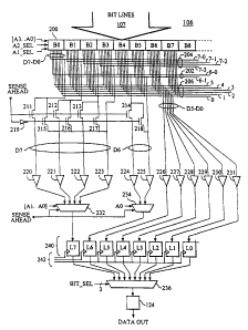
Fig. 2 shows a logic diagram of the Y decoder
circuit shown in Fig. 1 designed in accordance with the
present invention.
Figs. 3A and 3B show a typical implementation of
the decoder circuit shown in Fig. 2.
Figs. 4A - 4B are timing charts, showing the
relative timing of the address bits and the data bits in
accordance with various embodiments of the present invention.
Fig. 5 is a flow chart of the operation of the
present invention.
Figs. 6A - 6D show the active lines during
operation of the device in accordance with the invention.
Figs. 7A - 7E show an alternate embodiment of the
Y decoder of the present invention and the active lines
during its operation.
Fig. 8 shows a third embodiment of the Y decoder
in accordance with the present invention.
Fig. 9 is an implementation of the switching
circuit shown in Fig. 8.
BEST MODE OF CARRYING OUT THE INVENTION
The serial memory device 100 of Fig. 1 operates in
conformance with the SPI standard, though the invention does
not require the SPI interface and is readily adapted to
other bus standards such as the IZC or the Microwire
CA 02509624 1999-04-09
70622-92D
-4c-
standards. Serial memory 100 comprises external pads
including address/DATA IN pad 122 for serially inputting
address and data bits, DATA OUT pad 124 for serial data
output, and clock pad 126 for an externally provided clock
signal.
CA 02509624 1999-04-09
-5-
A memory matrix 102 comprises a plurality of
memory locations, organized into rows and columns. Each
row (aka page) of memory is addressed by an X portion of
the memory address, and each column of memory within a
page is addressed by a Y portion of the memory address.
Each column of memory consists of a set of bit lines 107,
typically eight bits, comprising the memory location.
The bit lines 107 from each column feed into a Y decoder
106.
For explanatory purposes only, it is assumed
that memory device 100 uses 16-bit addressing, and more
specifically that the X portion of the address occupies
the upper 12 bits A15 - A, and the Y portion occupies the
lower 4 bits A3 - Ao of the address word. It is further
assumed that each memory location is an eight-bit datum.
Thus, memory matrix 102 is a 4096 row X 16 column array,
each column consisting of eight bit lines. It should be
clear, however, that the invention can be readily scaled
up or down to accommodate other address sizes and
differently sized X and Y portions of the address word.
A data size other than eight bits can also be used.
Address/DATA IN pad 122 feeds into an address
buffering circuit 112. The address buffering circuit
provides the X portion of a target address and the Y
portion as well. The X portion of the address feeds into
an X decoder 104 which is coupled to memory matrix 102
and selects the specified memory page. The Y portion of
the address feeds into Y decoder 106 which selects the
specified memory location in the selected page. As will
be shown below, Y decoder 106 includes the sense
circuitry for sensing the bit lines of an accessed memory
location. Y decoder 106 further includes circuitry for
outputting the bits of the target location on DATA OUT
pad 124.
Address/DATA IN pad 122 accepts an externally
provided serial bit stream and feeds it into an input
buffer 108. As will be explained below, input buffer 108
includes circuitry for storing a bitstream to be written
CA 02509624 1999-04-09
-6-
to a page or a portion thereof. Control logic 110
provides control signals and timing signals for operating
the various components comprising the memory device 100.
The construction of Y decoder 106 will now be
discussed with reference to Fig. 2. The Y decoder of the
present invention comprises a decoder circuit 200 which
receives, as input, the eight bit lines 107 from each
column in memory matrix 102. Recall that for the purpose
of explanation the memory array is a 4096 row by 16
column array of eight-bit data. Thus, the number of bit
lines feeding into decoder circuit 200 is 128 (16 x 8).
Decoder circuit 200 includes a set of eight output data
lines D7 - DO for each byte in the array, namely bytes
BC - B15, thus providing a one-to-one mapping between the
incoming bit lines and the outgoing data lines.
Under the control of address control lines
A2_SEL and A1-SEL and address lines A3 - Ao, decoder
circuit 200 can be manipulated to behave as a 16-to-4
decoder, a 16-to-2 decoder or a 16-to-1 decoder. With
only A2-SEL asserted, the decoder circuit will output the
data lines of the four bytes whose upper two address bits
are equal to A3, A~. With only A1 SEL asserted, the
decoder circuit will output the data lines of the two
bytes whose upper three address bits are equal to A3, Az,
A,. Finally, when neither A2-SEL nor A1_SEL are asserted
decoder circuit 200 will produce the one byte addressed
by address bits A3 - Ao .
Turn now for a moment to Fig. 3A where a
typical implementation of decoder circuit 200 is shown.
Each byte has an associated chain of decoding transistors
402. Decoding of a given byte occurs by coupling its
decoding transistors to the appropriate address lines,
A3 - Ao and/or its complements. Each byte also has an
associated set of pass transistors 404 which gate its
corresponding data lines D7 - D0. The pass transistors
404 for a given byte are switched by the terminus line
401 of the decoding chain 402 corresponding to that byte.
Thus, for example, if address lines A3 - Ao are presented
CA 02509624 1999-04-09
-
with "0110" then the address will be decoded by the
decoding chain for byte 6, shown in bolded lines in Fig.
3A. Its corresponding pass transistors will be turned on
via the terminus line 401, thus passing its data lines
D7 - DO through to the output of decoder circuit 200.
As mentioned above the A2 SEL and A1 SEL
control lines modify the behavior of decoder circuit 200.
This is accomplished through the use of OR gates 410,
412. Address line A1 and the A2 SEL line feed into OR
gates 410. Address line AO and both the A2_SEL and
A1 SEL lines feed into OR gates 412. Address bits A1 and
AO represent the low order bits of the address. When
A2-SEL is asserted all four combinations of A1 and Ao are
forced, so that specifying bits A3 and A~ causes decoder
200 to output the following four bytes: A3,Az,0,0;
A3,A~, 0, 1; A3,A2, 1, 0; and A3,A2, 1, 1, irrespective of Al and
Ao. For example, Fig. 3B shows in bold lines the
activated bytes when A3=0, A2=1 and A2 SEL is asserted.
Hence, asserting A2-SEL causes decoder circuit 200 to
behave as a 16-to-4 decoder. Similarly, when A1 SEL is
asserted both combinations of the Ao address line are
forced. Thus, specifying A3, A2 and A1 will produce the
following two bytes: A3,AZ,A1, 0 and A3,A2,A1, 1. Hence,
asserting A1 SEL results in a 16-to-2 decoder.
Return now to the description of the Y decoder
106 shown in Fig. 2. The data lines of decoder circuit
200 are variously coupled to a four-wire bus 204, a
two-wire bus 202, and a six-wire bus 206. The four-wire
bus 204 consists of wires 7-0, 7-1, 7-2, and 7-3. The
two-wire bus 202 consists of wires 6-1 and 6-0. The
six-wire bus 206 consists of wires 5, 4, 3, 2, 1,
and 0.
Each wire of the four-wire bus 204 couples
together the most significant bit, namely the D7 data
line from decoder 200, of every fourth byte. Thus, wire
7-0 couples together the D7 data line of every fourth
byte beginning with byte B0. Wire 7-1 couples together
the D7 data line of every fourth byte beginning with byte
CA 02509624 1999-04-09
_8_
B1. Wire 7-2 couples together the D7 data line of every
fourth byte beginning with byte B2. Wire 7-3 couples
together the D7 data line of every fourth byte beginning
with byte B3. In the example where the array consists of
16 columns of bytes, the D7 bit of bytes B0, H4, B8, and
B12 are coupled together by wire 7-0; the D7 bit of bytes
B1, B5, H9, and B13 are coupled together by wire 7-1; the
D7 bit of bytes B2, B6, B10, and B14 are coupled together
by wire 7-2; and the D7 bit of bytes B3, B7, B11, and B15
are coupled together by wire 7-3.
Next is the two-wire bus 202. Here,. the data
line of the second mast significant bit (D6) of every
other byte is coupled to either the 6-0 wire or the 6-1
wire. Specifically, the second most significant data
line of every other byte starting with byte BO is coupled
to wire 6-0 and the second most significant data line of
every other byte starting with byte B1 is coupled to wire
6-1. Thus, the D6 line of the even bytes beginning with
BO are coupled to wire 6-0. Similarly, the D6 line of
the odd bytes are coupled to wire 6-1.
Finally, the six-wire bus 206 couples together
each of the six remaining data lines (D5 - DO) of every
byte. Thus, the D5 data line of each byte is coupled to
wire 5 of the six-wire bus, the D4 data line of each byte
is coupled to wire 4, the D3 data line of each byte is
coupled to wire 3, and so on as shown in Fig. 2.
Ignoring for the moment the routing through
transistors 211-218, Y decoder 106 further includes sense
circuitry (sense amps) 220 - 231, each having an input
coupled to a wire from one of the buses 202 - 206. Thus,
wire 7-0 of four-wire bus 204 is coupled to the input of
sense circuit 220 to read the data on wire 7-0. Similar-
ly, wire 7-1 of four-wire bus 202 is coupled to the input
of sense circuit 221 to read the data on wire 7-1, and so
on. ,Coupled in this manner, sense circuits 220 - 223
read out the most significant bit (D7) of every four
contiguous bytes, e.g. bytes BO - B3, B4 - B7, and so on.
In like manner, sense circuits 224 and 225 read out the
CA 02509624 1999-04-09
_g_
next most significant bit (D6) of every two contiguous
bytes, e.g. bytes BO & B1, B2 & B3, B4 & B5, and so on.
Finally, sense circuits 226 - 231 read out the remaining
bits (D5 - DO) of every byte.
The outputs of sense circuits 220 - 223 each
feeds into a 4:1 selector 232. Selector 232 is
controlled by address lines A1, Ao, the output of which
feeds into position L7 of latch 240. The outputs of
sense circuits 224 and 225 feed into a 2:1 selector 234.
Selector 234 is controlled by address line Ao, the output
of which feeds into position L6 of latch 240. Finally,
the outputs of sense circuits 226 - 231 each feeds into
respective positions L5 - LO of latch 240. Latch control
lines 242 are driven by control logic 110 to provide a
timed latch sequence for latching in data from the sense
circuits 220 - 231. The outputs of latch 240 feed into
an 8:1 selector 236, which is controlled by a selector
control BIT SEL. The output of selector 236 is coupled
to output pad 124.
Return now to transistors 211 - 218. Transis-
tors 211 - 214 couple the individual wires of four-wire
bus 204 and two-wire bus 202 to their respective sense
circuits. Transistors 215 - 217 couple all four wires of
four-wire bus 204 into sense circuit 223. Similarly,
transistor 218 couples the two wires of two-wire bus 202
into sense circuit 225. Transistors 211 - 214 are turned
on when control signal SENSE-AHEAD is HI, while
transistors 215 - 218 are turned on through inverter 219
when SENSE-AHEAD is LO.
In accordance with the SPI interface, the
address bits of the target memory location are serially
shifted in on each rising clock edge, starting with the
most significant bit. After clocking in the last address
bit the most significant bit of the target byte is
latched out on the falling clock edge immediately
following the last address bit.
Operation of the present invention will now be
described with reference to Figs. 1, 2, 4A, 4B, 5, and
CA 02509624 1999-04-09
-10-
6A - 6C. In Fig. 4A, each rising clock edge is
identified with respect to the address bit being clocked
in; for example, address bit Als is shifted in on the Als
clock, address Al, is shifted in on the Al, clock, and so
on.
Each address bit of the target is shifted in
serially until the high order bits A15 - A4 comprising the
X portion of the target address have been shifted in,
steps 502, 503. At clock A9 the X portion of the target
address is sent to the X decoder 104. This is
accomplished by properly buffering the incoming address
bits in address buffer circuit 112 and transmitting the X
portion to the X decoder when bits A15 - A4 have been
received. The row (page) in which the target byte is
located is therefore known. Next, the address bits of
the Y portion of the target address are shifted in while
the row is being selected by X decoder 104, steps 504A,
504B.
Page selection and receiving of the next
address bit are concurrent operations as represented in
Fig. 5 by the dashed line, identified as event Eo, passing
through steps 504A and 5048. Address bits are received
until the AZ bit has been shifted in, steps 5048, 505.
At the A2 clock shown in Fig. 4A address bits A;
and AZ have been received and address buffering circuit
112 feeds these two address bits into Y decoder 106.
Control logic 110 asserts A2-SEL to decoder circuitry 200
so that the data lines of the four bytes in the selected
row having the same A3, Az address bits are produced, step
506A. Assuming that the target byte is located in byte
position B5 of the selected row, i.e. A3, A2 are "O1",
bytes B4 ("0100"), B5 ("0101"), B6 ("0110"), and 87
("0111") axe produced. Control logic 110 also holds the
SENSE-AHEAD control line HI so that the four D7 data
lines of the four selected bytes are coupled to and.
sensed by the four sense circuits 220 - 223. At the same
time, the next address bit is shifted in, step 5068.
CA 02509624 1999-04-09
-11-
Event line E1 indicates the concurrency of these two
events.
Fig. 6A shows the active lines (highlighted) at
this time, illustrating the sensing of the D7 data lines.
It can be seen that sensing of the target byte B5 has
begun before the Y address is fully received. In effect,
a prediction of the target byte is being made based on
address bits A3 and A2, by sensing the D7 lines of these
four bytes. Although not highlighted in Fig. 6A, the
four D6 data lines of bytes B4 - B7 feed into the two D6
sense circuits 224, 225. At this time, however, the
output is indeterminate since each sense circuit is
reading the output of two data lines. The outputs of the
D5 - DO sense circuits, likewise, are inconsequential
since each is receiving four data lines from the four
selected bytes. Since the output of sense circuits 224 -
231 are indeterminate and thus serve no purpose at this
time, the sense circuits can be provided with enabling
circuits so that they may be turned off in order to
conserve power.
Upon receiving the A1 address bit at the Al
clock, control logic 110 asserts A1 SEL and de-asserts
A2 SEL to decoder circuit 200. This results in the
decoding of high order address lines A3 - A1, producing
the two bytes having in common those high order address
bits, namely "010" in the example where the target byte
is byte B5. Thus, bytes B4 and B5 are produced.
Consequently, only two of the original four D7 data lines
continue to be sensed, step 508A. In addition, sensing
now begins for the two D6 data lines of the two selected
bytes, step 508B. Prediction of the target byte
continues. Meanwhile, the Ao bit is being shifted in.
Event line EZ indicates the concurrency of these events.
Fig. 6B shows the active lines (highlighted) at
this time, illustrating the sensing of the D7-and the D6
data lines. As in Fig. 6A, sense circuits 2-26 - 231 each
receive data lines D5 - DO from bytes. B4 and BS and
therefore their outputs are indeterminate. Thus, sense
CA 02509624 1999-04-09
-12-
circuits 226 - 231 remain in the off condition. More-
over, circuits 222 and 223 can be disabled to conserve
power since the target byte is neither B6 nor H7.
At event E3, when the Ao bit is shifted in
during the Ao clock, control logic 110 de-asserts both the
A2 SEL and the A1 SEL lines so that decoder circuit 200
will produce the target byte that is addressed by
A3 - Ao, namely byte B5. This leaves only one of the
original D7 data lines, step 510A. Moreover, by this
time data line D7 will have been sensed and is ready to
be shifted out. Meanwhile, only one of the original two
D6 data lines remains selected and continues to be
sensed, step 510B. At the same time, parallel sensing
begins for data lines D5 - DO of the target byte, step
510C. Finally, selectors 232 and 234 select the sense
circuit outputs as determined by address bits A1 and Ao.
Control logic 110 signals latch lines 242 to sequentially
latch in D7, D6 and eventually D5 - D0. Fig. 6C
illustrates the active lines at this point in time. Note
that sense circuits 220 and 222 - 224 can be turned off
to conserve power, keeping active sense circuits 226 -
231.
At the falling edge following the Ao clock, data
line D7 of the target byte is shifted out, sensing of the
bit having begun five half-cycles earlier at clock A2.
Similarly data bit D6 is ready to be shifted out at the
next falling edge, shown in Fig. 4A and identified as the
D6 clock. Note that sensing of data line D6 also has
commenced five half-cycles earlier. Similarly, data line
D5 was sensed five half-cycles prior to being shifted
out. As to data lines D4 - D0, however, sensing of each
successive data line will occur for two half-cycles
longer than the previous data line. Thus, D4 will have
been sensed for seven half-cycles prior to being output,
while DO will have been sensed for fifteen half-cycles.
As previously discussed, prior art SPI-
compliant devices must complete row selection and data
sensing within the one-half cycle following receipt of
CA 02509624 1999-04-09
-13-
the last address bit in order to begin data output at the
falling edge. This one-half cycle is shown as t, in Fig.
4A. The predictive operating mode of the present
invention provides a two-fold improvement: first, row
selection begins as soon as the X portion of the address
is received; second, data sensing of the target byte
begins as soon as some of the Y address bits are clocked
in. The timing in Fig. 4A shows that the present
invention makes available at least five half-cycles of
time (tz) for sensing the data bits of the target byte.
Thus, the clock used in the present invention device can
run faster than that of prior art devices by a factor of
five. Actually, the factor is slightly higher than five
since, in the present invention, row selection occurs
prior to data sensing.
Continuing with the operation of the device,
consider the reading out of a subsequent byte. The
address buffering circuit 112 simply increments the
current address. In the first case, where the next byte
is on the same page, this simply involves incrementing
the Y portion of the address, the row remaining
unchanged. In the second case, where the next byte is or.
a new page, both the X portion and the Y portion of the
address change.
With reference to Fig. 6D, consider the first
case, where the next byte is on the same page as the
previous byte, namely byte B6. Control logic 110 now
de-asserts the SENSE-AHEAD line. This turns off
transistors 211 - 214 and turns on transistors 215 - 218,
thus feeding all of the D7 lines into sense circuit 223
and all of the D6 lines into sense circuit 225. Since
the invention is no longer in prediction mode at this
time, there is no longer any need to sense more than one
D7 or D6 line at a time and so A1 SEL and A2 SEL are de-
asserted. Thus, when the address is incremented to
select byte B6, only the eight data lines of B6 will feed
into their respective sense circuits_ Selectors 232 and
234 are further characterized by selecting sense circuits
CA 02509624 1999-04-09
-14-
223 and 225 respectively in response to de-assertion of
SENSE-AHEAD. Fig. 6D shows the active lines in this
situation. .
Turning to Figs. 4A - 4H, it can be seen that
after the D5 clock, when data bits D5 - DO are latched,
the sense circuits become available to sense the next
byte. Thus, in scenario A shown in Fig. 4B the address
is incremented sometime after the D5 clock. Shortly
thereafter data lines D7 - DO of the next byte are
sensed. This gives the next byte more than five
half-cycles of time to be sensed, so that at clock D7
shown in Fig. 4B, the D7 bic of the next byte is ready to
be Shifted out.
Consider next the case when the next byte is on
a new page. Again, the SENSE-AHEAD line is de-asserted
and the address in incremented. This time, the X and Y
portions of the address change. Thus, in scenario B of
Fig. 4B the address is incremented some time after the D5
clock. However, now a row select must now occur to
select the next page. Thus, the step of sensing the
first byte of a new page must be delayed for an amount of
time. As can be seen from the timing chart, the sensing
step can be delayed until the rising edge following the
D2 clock, roughly four half-cycles. This ensures that
five half-cycles are available for sensing the first byte
of the new page. In the preferred embodiment, however,
since row selection occurs almost immediately subsequent
to the address increment, data sensing of the next byte
can begin right away as indicated in Fig.~4B. In both
scenarios, plenty of clock cycles are available for a row
select and a sensing step because there is always one
byte that has already been sensed and stored in latch 240
that is being clocked out.
In the embodiment of the Y decoder shown in
Fig. 2, twelve sense circuits are used. Refer now to
Fig. 7A for a description of a Y decoder 106 in
accordance with the present invention which utilizes ten
sense circuits. As will become clear, the reduction in
CA 02509624 1999-04-09
-15-
sense circuits is made possible by re-using some of the
sense circuits during the decoding of the target byte.
Those parts of the Y decoder shown in Fig. 7A which are
the same in Fig. 2 retain their original reference
numerals. The decoding circuit 200 as shown in Figs. 2
and 3 is used in this embodiment.
Ignoring for the moment the sense-ahead
transistors 711 - 718, the four wire bus 204 and two wire
bus 202 are coupled to mux's 740 - 743. Each mux is a
2-to-1 selector having a left-side input line designated
as the "1" input, a right-side input line designated as
the °C" input, and a one-bit mux selector input 772.
When the mux selector input is asserted (i.e. HI) the "1"
input is produced at its output, and when the mux
selector is de-asserted (i.e. LO) the "0" input is
produced. This applies for mux's 740 - 761 shown in Fig.
7A.
The D7 data lines of four wire bus 204 are
coupled to the "1" input of mux's 740 - 74 3 as shown.
Specifically, the 7-0 wire is coupled to t he "1" input of
mux 740, the 7-1 wire is coupled to the "1" input of mux
741, the 7-2 wire is coupled to the "1" input of mux 742,
and the 7-3 wire is coupled to the "1" input of mux 743.
The two-wire bus 202, carrying t he D6 data
lines, are coupled in alternating fashion to the "0"
inputs of mux's 740 - 743. Thus, the 6-0 wire is coupled
to the "0" inputs of mux's 740 and 742, and the 6-1 wire
is coupled to the "0" inputs of mux's 741 and 743. The
six-wire bus 206 is coupled to sense circuits 226 - 231
as described above with respect to Fig. 2.
The output of each mux 740 - 743 feeds
respectively into sense circuits 720 - 723. The output
of each sense circuit in turn feeds into two mux's 750,
751. More specifically, sense circuits 720 and 721 feed
into the "1" and the "0" inputs of mux 750 respectively,
while sense circuits 722 and 723 feed into the "1" and
the "0" inputs of mux 751 respectively.
CA 02509624 1999-04-09
-16-
Finally, the outputs of mux's 750 and 751 are
cross-coupled to mux's 760 and 761. In particular, mux
750 is coupled to the "1" input of mux 760 and to the "0"
input of mux 761,~while mux 751 is coupled to the "1"
input of mux 761 and to the "0" input of mux 760. The
output of mux 760 feeds into the L7 latch of data latch
240 and the output of mux 761 feeds into the L6 data
latch. The L5 - LO data latches are coupled to the
outputs of sense circuits 226 - 231 respectively as
shown.
Mux controller 710 provides control signals
A - F which are coupled to the mux selector inputs 772 of
mux's 740 - 761. The control signals A - F are functions
of address bits A, - Ao, control lines A2_SEL and A1-SEL,
and the SENSE-AHEAD line. The signals A - F are defined
by the following logic equations:
A = A2-SEL ~ (-A2-SEL & -A1) ~ -SENSE-AHEAD,
2 0 B = A2-SEL ~ ( -.A2-SEL & -.A1 ) ,
C = A2-SEL ~ (-A2_SEL & A1 & SENSE-AHEAD),
D = A2-SEL ~ (-A2_SEL & Al) ,
E = -Ao ~ -SENSE-AHEAD, and
F = -A1 " -.SENSE-AHEAD,
where:
the symbol ~ is logical OR
the symbol & is logical AND;
the symbol -. means complement;
A2-SEL is true at the A2 clock; and
-A2-SEL is true at the A; and Ao clocks.
The sense-ahead transistors 711 - 718 serve the
same purpose as their counterparts shown in Fig. 2,
namely to control the flow of the D7 lines and the D6
lines during prediction mode operation and for
CA 02509624 1999-04-09
-17-
subs a quently and sequentially accessed memory locations.
In Fig . 7A transistors 711 - 718 are arranged such that
when SENSE-AHEAD is LO all the D7 lines feed into the "1"
input of mux 740 and all the D6 lines feed into the "0"
inpu t of mux 742.
In operation, the Y decoder 106 shown in Fig.
7A proceeds in accordance with the timing diagrams shown
in Figs. 4A and 4B. For the following discussion, refer
to Figs. 7B - 7E and assume the target location is byte
B6 (Y-portion of the target address, "0110") of the
selected row. As before, four candidate bytes are
produced by the decoder circuit 200 at the AZ clock,
namely bytes H4 - B7. With the SENSE-AHEAD line asserted
the sense-ahead transistors 711 - 713 are conductive,
sending the four D7 data lines of bytes B4 - B7 into the
«1" input of each mux 740 - 743. The A2 SEL line is
asserted at this time which, according to the above logi c
equations, causes mux controller 710 to assert control
signals A - D, thereby selecting the "1" input of mux's
740 - 743 and feeding the D7 lines into sense circuits
720 - 723. Fig. 7B shows the active lines.
At the A1 clock, decoder circuit 200 produces
bytes B6 and B7; i.e. those bytes having in common the
same high order address bits: A3 - A1, "011". A2 SEL is
deasserted at this time and since address bit A1 is "1",
mux controller 710 asserts control signals C and D to
select the "1" input of mux's 742 and 743. Consequently,
m~~s 742 and 743 continue to feed the D7 lines of bytes
B6 and B7 into sense circuits 722 and 723, while data
lines D7 of bytes B4 and B5 are decoupled from sense
circuits 720 and 721. Although the idea of decoupling a
data line from its sense circuit while the data is being
sensed seems counterintuitive, the D7 lines of bytes B4
and B5 are no longer needed, since it is known at this
time that neither of bytes B4 and B5 is the target byte.
These sense circuits can therefore be re-used. Since A
and B from mux controller 710 are LO, the "0" input of
m~~s 740 and 741 are selected to feed the D6 data lines
CA 02509624 1999-04-09
-18-
of bytes B6 and B7 into sense circuits 720 and 721, thus
re-using the circuits. Fig. 7C shows the active lines.
At the Ao clock, the address of the target byte
is completely known and decoder circuit 200 therefore
produces byte B6. Control signals A - D remain unchanged
from clock A1. In addition, mux controller 710 asserts
the E and F control lines. The E control line is a
function of Ao, selecting a line from each of the D6 and
D7 pairs by operating mux's 750 and 751. In this case,
since Ao is "0", the "1" inputs of mux's 750, 751 are
selected, thus producing the D6 and D7 lines from byte
B6. Control line F operates mux's 760 and 761 to switch
the D6 and D7 lines so that they feed into their
appropriate positions in latch 240. The F signal is
based on the A, address bit, since this bit determines how
mux's 740 - 743 are paired off between the D6 and D7 data
lines. Fig. 7D shows the active lines, including the
D5 - DO data lines.
Finally, for subsequently accessed memory
locations, the SENSE-AHEAD line is deasserted. This ties
together the four wires 7-0 through 7-3 of four-wire bus
204 by virtue of transistors 711 - 713 being turned off
and transistors 715 - 717 being turned on, feeding the
wires into the "1" input of mux 740. Similarly, the two
wires 6-0 and 6-1 are tied together through transistor
718 and fed into the "0" input of mux 742. Mux
controller 710 selects the "1" input of mux's 740, 750
and 760 to teed the D7 line into sense circuit 720 into
latch L7. Similarly, mux controller 710 selects the "0"
input of mux 742 to feed the D6 line into sense circuit
722, and from there the "1" input of mux's 751 and 761
are selected to send the D6 line into the L6 latch. Fig.
7E shows the data flow for the subsequent byte, namely
byte B7.
The embodiments of the invention shown in. Fig.
2 and Fig. 7A respectively use twelve and ten sense
circuits. The reduction of sense circuits achieved by
the embodiment of Fig. 7A comes about by the use of
CA 02509624 1999-04-09
-19-
multiplexing circuitry to selectively switch the data
lines to certain sense circuits when they become
available as subsequent bits of the address are clocked
into t he memory device.
Fig. 8 shows an embodiment which extends the
principle of re-using sense circuits another step.
Elements previously introduced and discussed in Figs. 2
and 7A retain their reference numerals. Fig. 8
introduces an additional set of mux's 850 - 853. These
mux's have three inputs: a "2" input, a "1" input, and a
"0" input. Each mux 850 - 853 also has a two-bit
selector input 874, where a "10" on selector input 874
produces the "2" input, a "O1" on selector input 874
produces the "1" input, and a "00" on selector input 874
produces the "0" input.
The "2" inputs of mux's 850 - 853 are coupled
respectively to the output of each mux 740 - 743. The
"2" inputs therefore receive either a D7 data line or a
D6 data line, depending on the selections made in mux's
740 - 743. The "1" and "0" inputs of mux's 850 - 853
are coupled respectively to the number 5 and number 4
wires of bus 206. The outputs of mux's 850 - 853 feed
into inputs of sense circuits 820 - 823. As will be
explained below, the presence of mux's 740 - 743 and 850
- 853 allow data lines D7, D6, D5 and D4 of the target
byte to feed into the sense circuits, while still
providing the predictive operating mode of the present
invention.
The outputs of the sense circuits feed into
inputs M - P of switching circuit 860. The outputs Q - T
of switch 860 respectively feed into the D7 - D4 latches
of data latch 240. Switching circuit 860 allows any
input M - P to be switched to any output Q - T under the
control of an eight-bit control line 860. Fig. 9 shows
an implementation of such a switch.
Mux controller 810 provides control signals
A - I which are coupled to mux selector inputs 872, 874,
and 876. The control signals are functions of address
CA 02509624 1999-04-09
-20-
bits A, - Ao, control lines A2 SEL and A1 SEL, and the
SENSE-AHEAD line. The signals A - I are defined by the
following requirements for the non-predictive mode of
operation, when SENSE-AHEAD is de-asserted: Pass
transistors 711 - 713 are off and pass transistors 715 -
717 are on, thus tying together all the D7 data lines and
feeding them into input "1" of mux 740. Likewise, pass
transistor 714 is off and pass transistor 718 is on, thus
tying together all the D6 data lines and feeding them
into the "0" input of mux 742. Thus, in the
non-predictive mode of operation, control signals A - I
are asserted so that mux 740 produces its "1" input, mux
850 produces its "2" input, and switch 860 routes its M
input to its Q output, resulting in the passage of data
line D7 to the D7 data latch through sense circuit 820.
Similarly, mux 742 produces its "0" input, mux 852
produces its "2" input and switch 860 routes its O input
to its R output, resulting in the passage of data line D6
to the D6 data latch through sense circuit 822. At the
same time, the number 5 wire of bus 206, which corres-
ponds to the D5 data line, is routed through input "1" of
mux 851 and coupled from input N of switch 860 to output
S, so that the D5 data line is latched into the D5 latch
through sense circuit 821. Finally, the number 4 wire of
bus 206, which corresponds to the D4 data line, is routed
through the "0" input of the 853 mux and coupled from
input P of switch 860 to output T and hence into data
latch D4 through sense circuit 823.
The control signals A - I of mux controller 810
are further defined by the following requirements during
the predictive mode of operation (see also the timing
chart of Fig. 4A), when SENSE-AHEAD is asserted: At the
AZ clock, when the four possible bytes are selected, mux
740 - 743 each produce its "1" input and mux's 850 - 853
each produce its "2" input, thus presenting the four D7
data lines to their respective sense circuits 820 - 823
whereupon data sensing begins.
CA 02509624 1999-04-09
-21-
At the A1 clock and depending on the A1 address
bit, one pair of mux's, either mux's 740 and 741 or mux's
742 and 743, will continue to produce the "1" input, thus
feeding two of the D7 lines to the next level of mux's.
The other pair will be switched to produce the "0"
inputs, which now carry the two possible D6 data lines.
Mux's 850 - 853 continue to produce the "2" inputs. The
effect is that two of the sense circuits will continue to
sense the D7 data lines, while the D7 lines will have
been de-coupled from the other two sense circuits in
order to begin sensing the D6 data lines.
At the Ao clock, when all the address bits are
in, the target byte will be known and selected by decoder
circuit 200. Two of the four mux's 850 - 853 will be
switched to produce the number 5 and number 4 wires of
bus 206 and sensing of the D5 and D4 data lines will
commence. At the same time sensing of the D3 - DO will
also commence with sense circuits 824 - 827. Meanwhile,
sensing of the D7 data line of the target byte will have
completed and will be ready for output, and the D6 data
line continues to be sensed. Finally, switch 860 is
operated via control line 876 to provide the necessary
cross-switching of inputs M - P to outputs Q - R to
ensure that data lines D7 - D4 are latched into their
corresponding data latches.
The embodiments shown in Figs. 2A, 7A, and 8
show that by the appropriate use of multiplexing
circuitry, the sense circuitry requirements can be
reduced. Alternative designs are possible, each having
varying degrees of complexity and silicon real-estate
requirements. The embodiment of Fig. 2A is straight-
forward, but requires twelve sense circuits. The
embodiment of Fig. 8 uses eight sense circuits, but
requires additional mux's and a more complex controller
to operate the mux's. Although the disclosed embodiments
provide predictive sensing at the AZ clock, the operation
can begin at an earlier clock to realize even greater
speed increases. The particular implementation approach
CA 02509624 1999-04-09
-22-
will depend on making tradeoffs among factors including
desired speed of the device, circuit complexity, memory
size, die size, and power requirements.
The disclosed embodiment of the invention
realizes a factor of five decrease in the time between
clocking in the last bit of the target memory location
and clocking out the first bit of the target, thus
permitting a five time increase in clock speed. However,
the principles disclosed herein can be used to realize a
factor of seven decrease in time. In the foregoing
discussion, the Y portion of the address consists of four
bits, and the predictive operating mode of the invention
begins after receiving the second bit of the Y portion.
With respect to Fig. 4A, if prediction mode begins after
receiving the first bit instead, then sensing of the D7
data line would begin on the A3 clock, thus decreasing the
time by a factor of seven. Necessary changes to the
logic include modifying decoder circuit 200 to provide
16-to-8 eight decoding in addition to the three decoding
modes described; the reason being that at the A3 clock
there will be eight candidate bytes. In addition, extra
sense amps will be needed. Following the architecture of
Fig. 2, eight sense amps will be required to sense the
eight candidate D7 data lines, four sense amps will be
needed to sense the four candidate D6 data lines, two
sense amps to sense the two possible D5 data lines, and
five sense amps to sense the D4 - DO data lines of the
target byte; a grand total of nineteen sense amps.
Following the architectures of Figs. 7A and 8, this
number of sense amps can be reduced with the use of
additional mux's to re-use sense amps which become
available as the number of candidate targets decreases
when additional address bits of the Y portion of the
target address become available. On the one hand, the
need for so many sense amps might be a deterrent to this
approach. On the other hand, the time decrease might
allow the use of slower but simpler (and thus smaller)
CA 02509624 1999-04-09
-23-
sense amps which can offset the size requirement of
having an increased number of sense amps.
Alternatively, the predictive operating mode
can be delayed until all but the last bit of the target
address has been clocked in. Thus with reference to Fig.
4A, sensing of the D7 data line will not commence until
the A, clock, when bits A3 - A1 are known. At that point,
there are only two candidate bytes and so only two
candidate D7 data lines to sense. In this configuration,
nine sense amps are needed to realize a factor of three
decrease in the time between receiving the target address
and outputting the target memory location, which
translates to a three time increase in the clock.
In the disclosed embodiment of the invention,
only one bit is sensed ahead of time for each address bit
received. Thus, with reference to Figs. 2 and 4A, when
address bit A2 is received on the A~ clock, predictive
sensing of the four candidate D7 data lines begins. Upon
receiving the next address bit, A;, predictive sensing of
the two candidate D6 data lines commences. In another
embodiment of the invention, however, more than one data
line per candidate byte can be sensed ahead of time
without departing from the scope and spirit of the
invention. For example, at the Az clock both the D7 and
D6 data lines of the four candidate bytes can be sensed.
As a matter of convention, the preferred
embodiment of the invention performed is predictive
operation on the least significant bits of the target
address, namely the Y portion of the address. However,
the invention is readily adapted to operate on the most
significant portion of the address instead, without
departing from the principles of operation of the
invention and without sacrificing the benefits made
possible by the invention.
In accordance with requirements of the SPI
protocol, the preferred embodiment of the invention
operates on the most significant bits of the candidate
bytes. Thus, the D7 data lines are sensed before sensing
CA 02509624 1999-04-09
-24-
the D6 data lines and so on. This allows for the most
significant bit to be shifted out first, per the SPI
protocol. Alternatively, for a protocol other than S PI,
the invention can be implemented to operate on the 1 east
significant bits first so that the least significant bit
is outputted first. Thus, the DO data lines of the
candidate bytes can be sensed first, followed by the D1
data lines, and so on. This approach is consistent with
the principles of operation of the invention and enjoys
the same benefits as achieved by the embodiment of the
invention disclosed above. With reference to Figs. 2 and
3A, the logic comprising decoder circuit 200 can be
adapted so that the bit zero lines are coupled to the D7
data lines, the bit one lines are coupled to the D6 data
lines, the bit two lines are coupled to the D5 data lines
and so forth, so that the low order bits of the candidate
bytes are sensed first.