Note: Descriptions are shown in the official language in which they were submitted.
CA 02509912 2005-06-13
WO 2005/018798 PCT/JP2004/011863
1
D E S C R I P T I 0 N
JUNCTION SUBSTRATE AND METHOD OF
BONDING SUBSTRATES TOGETHER
Technical Field
The present invention relates to a junction
. substrate composed of a plurality of substrates and
a method of bonding the substrates together.
Background Art
In recent years, small-sized reactors called
microreactors have been developed. The microreactor is
a small-sized reactor in which a plurality of reactants
such as materials and reagents are allowed to react
with each other while being mixed together. The
microreactor is utilized to carry out chemical reaction
experiments in micro areas, develop drugs, or develop
artificial organs or is utilized as a genome and DNA
analysis tool or a basic analysis tool for microfluid
engineering. Chemical reactions using the microreactor
have characteristics not exhibited by normal chemical
reactions using beakers or flasks. For example, the
microreactor is advantageous in that the whole reactor
is so small as to provide a very high effectiveness of
regenerator to allow efficient temperature control
required for reactions. Thus, the microreactor makes
it possible to quickly and easily accomplish reactions
requiring precise temperature control or rapid heating
CA 02509912 2005-06-13
WO 2005/018798 PCT/JP2004/011863
2
or cooling.
Specifically, the microreactor is formed with,
for example, a channel through which reactants flow
and a reactor in which reactants react with each other.
In Jpn. Pat. Appln. KOKAI Publication No. 2001-228159,
a silicon substrate in which a groove with
a predetermined pattern is formed is anodically bonded
to a Pyrex (registered trade mark) substrate so that
they are laminated to each other. A channel is then
formed in a closed area between the two substrates.
The "anodic bonding" is a bonding technique to apply
a high voltage to substrates in a high-temperature
environment to generate an electrostatic attraction
between the substrates, thus chemically binding the two
substrates together at an interface. The anodic
bonding is particularly excellent among substrate
bonding techniques because the substrates can be
strongly bonded together without using any coating
agent and in the atmosphere. '
Some microreactors are provided with heating means
for heating a channel in order to facilitate reactions
in the reactor. For example, it is contemplated that
to transfer heat to a channel portion via a substrate,
a heating resistant film corresponding to the channel
pattern and an interconnect made of metal to supply
power to the heating resistant film may be formed on
a side of a front surface of a glass substrate or
CA 02509912 2005-06-13
WO 2005/018798 PCT/JP2004/011863
3
the like (the surface of the substrate which is
opposite the surface bonded to a silicon substrate).
In this case, when the glass substrate and the silicon
substrate are anodically bonded together via the
heating resistant film and interconnect, electric
fields concentrate in parts of the front surface of the
glass substrate which are close to the heating
resistant film and interconnect. Consequently, Na from
the glass substrate is locally precipitated in these
parts. As a result, Na may enter the heating resistant
film and/or the interconnect, deposited on the heating
resistant film in order to apply a voltage to the
heating resistant film. These impurities may create
fine gaps in the heating resistant film, interconnect
film and/or its front surface to make it rough.
Consequently, the heating resistant film and/or the
interconnect film may be peeled off from the glass
substrate or a metal electrode may be peeled off from
the heating resistant film.
The present invention is advantageous in that when
a glass substrate or the like which contains Na is
anodically bonded to another substrate, Na from the
substrate is hindered from being locally precipitated.
Disclosure of Invention
According to an aspect of the invention, there is
provided a junction substrate comprising: a first
substrate having one and opposite surfaces; a buffer
CA 02509912 2005-06-13
WO 2005/018798 PCT/JP2004/011863
4
film formed on the one surface of the first substrate;
a metal containing film formed on the buffer film and
having a lower resistance than the buffer film; and a
second substrate bonded to the opposite surface of the
first substrate.
According to this aspect, the buffer film formed
on the predetermined surface of the first substrate can
hinder Na moved by anodic bonding from reaching the
metal containing film. In particular, when the buffer
film is wider than the metal containing film, it is
possible to prevent electric fields resulting from the
anodic bonding from being dispersed to moue and
concentrate Na near the metal containing film.
Consequently, the metal containing film can be
prevented from being degraded by Na.
A groove may be formed in at least one of
the first and second substrates. The first substrate
may be a glass substrate. The first and second
substrates are preferably anodically bonded together.
The metal containing film may be a member heated when
a predetermined voltage is applied to the film.
The buffer film is suitably composed of a Ta-Si-0-
based material. The metal containing film is suitably
composed of a Ta-Si-0-N-based material.
The buffer film desirably has a high resistance
enough to suppress the concentration of electric fields
in the metal containing film. The metal containing
CA 02509912 2005-06-13
WO 2005/018798 PCT/JP2004/011863
film desirably has a sheet resistance that is
one-thousandth or less of that of the buffer film.
The junction substrate is also applicable to a
microreactor. The buffer film preferably has a larger
5 area than the metal containing film.
According to the other aspect of the invention,
there is provided a method of bonding a plurality of
substrates together to obtain a junction substrate, the
method comprising: forming a heating resistant film
with a predetermined pattern on a buffer film formed on
one surface of a first substrate; abutting the first
substrate against a second substrate at the other
surface of the first substrate which is opposite the
one surface on which the buffer film is formed; and
applying a voltage so that the first substrate operates
as a negative electrode while the second substrate
operates as a positive electrode, to anodically bond
the first and second substrates together.
According to this aspect, the first and second
substrates are anodically connected together after the
buffer film has been formed on the predetermined
surface of the first substrate. Accordingly, the
buffer film can hinder Na moved by anodic bonding from
reaching the heating resistant film. In particular, if
the buffer film is wider than the predetermined pattern
on the heating resistant film, when a voltage is
applied to between an anode and a cathode, an electric
CA 02509912 2005-06-13
WO 2005/018798 PCT/JP2004/011863
6
field from the cathode is widely dispersed through the
buffer film. This results in a uniform field intensity
between the anode and the cathode. Therefore, the
distribution of the electric field is not biased.
In the above bonding method, the heating resistant
film may have a meandering shape having a plurality of
longitudinal portions. If the width of each
longitudinal portion is defined as LA, the length of
each longitudinal portion is defined as Lg, the spacing
between the adjacent longitudinal portions is defined
as LC, the sheet resistance of each longitudinal
portion is defined as Sh, and if the sheet resistance
of a part of the buffer film which is exposed from
between the adjacent longitudinal portions is defined
as Sf, the relationship Sh X (Lg/LA) X ~ X 100 <
Sf X (LC/Lg) may be met.
When the resistance of the two adjacent
longitudinal portions is expressed as Sh X (Lg/LA) X
2, the resistance of a part of the buffer film which is
exposed from between these two longitudinal portions is
expressed as Sf X (LC/Lg), and these two resistances
meet the relationship Sh X (Lg/LA) 2 X 100 < Sf
(LC/Lg), the resistance of the part of the buffer film
which is exposed from between the two longitudinal
portions is much higher than that of the two
longitudinal portions. When a voltage is applied to
both ends of the heating resistant film, a current is
CA 02509912 2005-06-13
WO 2005/018798 PCT/JP2004/011863
7
unlikely to flow through the buffer film but is likely
to flow through the heating resistant film.
According to further aspect of the invention,
there is provided a method of bonding a plurality of
substrates together to obtain a junction substrate,
the method comprising: forming an interconnect film
with a predetermined pattern which supplies power to
a heating resistant film formed on one surface of
a first substrate; abutting the first substrate against
a second substrate at the other surface of the first
substrate which is opposite the surface on which the
heating resistant film is formed; and applying
a voltage so that the first substrate operates as
a negative electrode while the second substrate
operates as a positive electrode, to anodically bond
the first and second substrates together.
With the method according to this aspect, the
heating resistant film formed on the predetermined
surface of the first substrate can hinder Na moved by
anodic bonding from reaching the metal containing film.
Consequently, the metal containing film can be
prevented from being degraded by Na. In particular,
when the heating resistant film is wider than the metal
containing film, it is possible to prevent electric
fields resulting from the anodic bonding from being
dispersed to move and concentrate Na near the metal
containing film.
CA 02509912 2005-06-13
WO 2005/018798 PCT/JP2004/011863
According to further aspect of the invention,
there is provided a method of bonding a plurality of
substrates together to obtain a junction substrate,
the method comprising: forming a heating resistant film
on a buffer film formed on one surface of a first
substrate; forming an interconnect film with
a predetermined pattern on the heating resistant film,
through which power is to be supplied to the heating
resistant film; abutting the first substrate against
a second substrate at the other surface of the first
substrate which is opposite the surface on which the
buffer film is formed; and applying a voltage so that .
the first substrate operates as a negative electrode
while the second substrate operates as a positive
electrode, to anodically bond the first and second
substrates together.
with the method according to this aspect, the
first and second substrates are anodically bonded
together after the buffer film has been formed on
the predetermined surface of the first substrate.
Accordingly, the buffer film can hinder Na moved by
anodic bonding from reaching the heating resistant film
and interconnect film. In particular, if the buffer
film is wider than the predetermined pattern on the
heating resistant film, when a voltage is applied to
between an anode and a cathode, electric fields from
the cathode are dispersed through the buffer film.
CA 02509912 2005-06-13
WO 2005/018798 PCT/JP2004/011863
9
This results in a uniform~field intensity between the
anode and the cathode. Therefore, the distribution of
electric fields is not biased. This in turn prevents
the localization of Na and thus the local degradation
of the heating resistant film and interconnect film.
Brief Description of the Drawings
FIG. 1 is a perspective view of a substrate in
which a groove as a concave portion is formed;
FIG. 2 is a sectional view taken along a line
(II)-(II) in FIG. 1 in a thickness direction;
FIG. 3 is a sectional view taken along a line
(III)-(III) in FIG. 1 in the thickness direction;
FIG. 4 is a perspective view of a substrate to be
bonded to the substrate shown in FIG. 1;
FIG. 5 is a sectional view taken along a line
(V)-(V) in FIG. 4 in a thickness direction;
FIG. 6 is a plan view of the substrate shown in
FIG. 4;
FIG. 7 is a sectional view showing an anodic
bonding;
FIG. 8 is a diagram illustrating the distribution
of field intensities in connection with an anodic
bonding according to a comparative example;
FIG. 9 is a graph showing the composition of
a front surface of a glass substrate film in its
thickness direction during anodic bonding according to
the present invention;
CA 02509912 2005-06-13
WO 2005/018798 PCT/JP2004/011863
FIG. 10 is a diagram illustrating the distribution
of field intensities during an anodic bonding according
to the present invention;
FIG. 11 is a graph showing the composition of
5 a front surface of a buffer film in its thickness
direction during anodic bonding according to the
present invention;
FIG. 12 is a sectional view showing an anodic
bonding according to a second embodiment of the present
10 invention;
FIG. 13 is a plan view of a substrate according to
the second embodiment;
FIG. 14 is a sectional view showing an anodic
bonding according to a third embodiment of the present
invention;
FIG. 15 is a diagram illustrating the distribution
of field intensities during an anodic bonding according
to the third embodiment;
FIG. 16 is a block diagram of a generation system
to which an anodically bonded microreactor according to
the present invention is applied;
FIG. 17 is a sectional view showing a generation
module in the generation system; and
FIG. 18 is a perspective view of the generation
system.
Best Mode for Carrying Out the Invention
With reference to the drawings, description will
CA 02509912 2005-06-13
WO 2005/018798 PCT/JP2004/011863
11
be given of the best modes for carrying out the present
invention. However, the scope of the present invention
is not limited to the illustrated examples.
[First Embodiment]
Description will be given of a first embodiment of
a method of bonding substrates together according the
present invention. FIG. 1 is a perspective view
illustrating a substrate to be bonded to another.
Specifically, the substrate 4 is composed of,
for example, a silicon substrate or glass substrate
having one surface 4A coated with a thin conductive
film. The substrate 4 has a predetermined thickness
and is rectangular. The surface 4A and an opposite
surface 4B are formed to be flat and parallel to each
other. The substrate 4 has a concave portion 5 formed
in the surface 4A and composed of one groove meandering
zigzag. An inlet 7 is formed at one end of the groove
so as to penetrate the substrate 4 in its thickness
direction. An outlet 8 is formed at the other end of
groove so as to penetrate the substrate 4 in its
thickness direction. A fluid flows into the inlet 7
and flows out of the outlet 8.
In a first step of a method of processing the
substrate 4, a predetermined mask is used to pattern
the concave portion 5, constituting a groove of depth
0.1 to 1.5 mm, by mechanical etching such as sand blast
or chemical etching using an etchant. Similarly, both
CA 02509912 2005-06-13
WO 2005/018798 PCT/JP2004/011863
12
ends of the groove are mechanically or chemically
etched to form through-holes constituting the inlet 7
and outlet 8. If glass is used as the substrate 4,
an oxidized film may be formed on the surface 4A so as
to be oxidized during an anodic bonding, described
later. In this case, a protective film is coated on
the oxidized film so as to prevent the oxidized film
being oxidized when the concave portion 5, the inlet 7,
and the outlet 8 are formed. FIG. 2 is a sectional
view of the substrate 4 taken along a line (II)-(II) in
FIG. 1 in the thickness direction of the substrate 4.
FIG. 3 is a sectional view of the substrate 4 taken
along a line (III)-(III) in FIG. 1 in the thickness
direction of the substrate 4.
As shown in FIG. 4, a glass substrate 1 to be
bonded to the substrate 4 has a buffer film 2 coated
all over its surface 1A. A meandering heating
resistant film 3 is provided on a front surface of the
buffer film 2. An opposite surface 1B of the glass
substrate 1 is anodically bonded to the surface 4A of
the substrate 4.
Like the case of the substrate 4, the surfaces 1A
and 1B of the glass substrate 1 are formed to be flat
and parallel to each other and are designed so that the
entire surface 1b abuts against the surface 4A of the
substrate 4. Specifically, the glass substrate 1 is
made of Pyrex (made by CORNING) containing several o of
CA 02509912 2005-06-13
WO 2005/018798 PCT/JP2004/011863
13
Na20 or soda-lime glass. FIG. 5 is a sectional view of
the substrate 1 taken along a line (V)-(V) in FIG. 4 in
the thickness direction of the substrate 1. The buffer
film 2 has a larger film formation area than the
heating resistant film 3.
A first step of a method of processing the glass
substrate 1 comprises forming the buffer film 2 on a
bottom surface of the glass substrate 1 so as to cover
almost the entire bottom surface. The buffer film 2 is
set to have a sheet resistance (surface resistance
rate) higher than that of the heat resistant film 3,
specifically, a sheet resistance set at of 1 to
1000 MS2/0. Preferably, such a material which has a
high resistance and which is not degraded under high
temperature during an anodic bonding is, for example, a
compound material composed of Ta, Si, and 0
(hereinafter referred to as a "Ta-Si-O-based material")
or a compound material composed of Ta, Si, 0, and N
(hereinafter referred to as a "Ta-Si-O-N-based
material").
To form the buffer film 2, the glass substrate 1
is first set in a sputtering apparatus as a target to
be coated. Subsequently, a Ta plate in which Si has
been buried (Ta:Si=3:1) is used as a target to carry
out sputtering in an atmosphere composed of an Ar gas
and an 02 gas. In the sputtering step, ions collide
against the target to emit secondary ions from the
CA 02509912 2005-06-13
WO 2005/018798 PCT/JP2004/011863
14
target. .The emitted secondary ions collide against the
bottom surface of the glass substrate 1 to form the
buffer film 2 of the Ta-Si-0-based material on the
bottom surface of the glass substrate 1. If a Ta-Si-O-
N-based material is manufactured, a target composed of
a Ta plate in which Si has been buried may be used in
an atmosphere composed of an Ar, 02, and N2 gases.
Once the buffer film 2 has been formed, the
meandering heating resistant film 3, which is heated
when a voltage is applied to the film 3, is formed on
a front surface of the buffer film. The heating
resistant film 3 is formed to have a lower sheet
resistance than the buffer~film 2 and preferably has
a sheet resistance one-thousandth or less of that of
the buffer film 2. Provided that the buffer film 2 is
a Ta-Si-O-based material, a heating resistant film 3
may be formed by Ta-Si-O-based material, for examples,
having a sheet resistance of about 100 to 1,000 S2/~.
Provided that the buffer film 2 is a Ta-Si-0-N-based
material, metal such as CU or Pt which is 0.01 to 1 S2/~
in sheet resistance may be used to form the heating
resistant film 3.
A method of forming the heating resistant film 3
by the Ta-Si-O-based material into is executed in
almost the same manner as that used to form the buffer
film 2. That is, a plate formed of Ta and in which Si
has been buried (Ta:Si=3:1) is prepared as a target.
CA 02509912 2005-06-13
WO 2005/018798 PCT/JP2004/011863
The glass substrate 1 is then set in the sputtering
apparatus so that the buffer film 2 is to be coated.
Then, sputtering is carried out in an atmosphere
composed of an Ar, 02, and N2 gases while using a mask
5 with a meandering opening to cover the buffer film 2.
In the step of forming the heating resistant
film 3, a well-known photolithography technique may be
used to form the heating resistant film 3 on the bottom
surface of the buffer film 2. The heating resistant
10 film 3 may then be patterned to meander.
Where the heating resistant film 3 is formed, the
heating resistant film 3 may be patterned to meander
along the concave portion 5 when the glass substrate 1
is laminated to the substrate 4 in which the meandering
15 concave portion 5 is formed. Further, provided that
the heating resistant film 3 is formed so as to cover
the concave portion 5, it may be rectangular or have
any other shape. Once the glass substrate 1 and the
substrate 4 are bonded together, the concave portion 5
may be allowed to function as a channel through which a
fluid composed of a mixture of one or more types of
materials flows. In this case, when the heating
resistant film 3 is formed to meander along the concave
portion 5, the interior of the channel in the concave
portion 5 can be uniformly and efficiently heated.
The heating resistant film 3 is preferably wider than
the corresponding portion of the concave portion 5.
CA 02509912 2005-06-13
WO 2005/018798 PCT/JP2004/011863
16
The step of forming the heating resistant film 3
allows the heating resistant film 3 to be patterned to
generally meander so that a plurality of longitudinal
portions 3a each having a predetermined length and
width are connected together by latitudinal portions 3a
as shown in FIG. 6. The longitudinal portions 3a
extend perpendicularly to the latitudinal portions 3b.
Here, the longitudinal resistance of each
longitudinal portion 3a of the heating resistant film 3
is defined as Sh. The width of each longitudinal
portion 3a is defined as LA. The length of each
longitudinal portion 3a is defined as Lg. The spacing
between the adjacent longitudinal portions 3a is
defined as LC. The sheet resistance of a part of the
buffer film 2 which is exposed from between the two
longitudinal portions 3a is defined as Sf. Then, the
resistance of a part of the heating resistant film 3
between points X1 and X2 on a line parallel to
a direction in which the latitudinal portions 3b of the
heating resistant film 3 extend is generally expressed
as Sh X (Lg/LA) >C 2. The resistance of the part of
the buffer film 2 between the points X1 and X2 is
expressed as Sf X (LC/Lg).
In the first embodiment, the buffer film 2 and
the heating resistant film 3 are desirably formed on
the glass substrate 1 so that the longitudinal
resistance of the two adjacent longitudinal portions 3a
CA 02509912 2005-06-13
WO 2005/018798 PCT/JP2004/011863
17
and the resistance of the part of the buffer film 2
which is exposed from between the two longitudinal
portions 3a meet Equation (1), shown below.
Sh X (LB/LA) X 2 >C 100 < Sf X (LC/LB) ... (1)
On the basis of Equation (1), the buffer film 2
and the heating resistant film 3 are formed on the
glass substrate 1 so that the resistance of the part of
the heating resistant film 3 between the points X1 and
X2 is one-hundredth or less of that of the part of the
buffer film between the points X1 and X2. Then, when
a voltage is applied to between both ends 3c and 3d of
the heating resistant film 3, a current is sufficiently
hindered from flowing through a part of the buffer film
2 between the points X1 and X2 which has a shorter
minimum distance than the heating resistant film 3.
On the other hand, a current is sufficiently allowed to
flow through the heating resistant film 3, which can
thus be heated efficiently.
Once the substrate 4 in which the concave portion
5 is formed and the glass substrate 1 on which the
buffer film 2 and the heating resistant film 3 are
formed have been respectively prepared, the steps
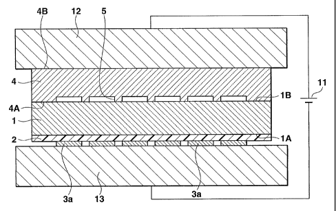
described below are executed as shown in FIG. 7. The
surface 4A of the substrate 4 is abutted against the
top surface 1B of the glass substrate 1 (the surface
opposite to the one on which the buffer film 2 and the
heating resistant film 3 are formed). A positive
CA 02509912 2005-06-13
WO 2005/018798 PCT/JP2004/011863
18
electrode 12 of an anodic bonding device 11 is
connected to the surface 4B of the substrate 4 to allow
the substrate 4 to operate as an anode. At this time,
the substrate 1 and the buffer film 2 are not in direct
contact with a negative electrode 13. In this state,
the substrates 1 and 4 are heated to 300 to 500°C.
Then, the anodic bonding device 11 applies a voltage of
300 to 1,000 V to the substrates 1 and 4 to anodically
bond them together. At this time, the negative
electrode 13 is in contact with the entire surface of
the heating resistant film 3 including the longitudinal
portions 3a and the latitudinal portions 3b in order
to maximize the area of contact with the glass
substrate 1. Thus, oxygen atoms present near the
surface lA of the glass substrate 1 are chemically
bonded to atoms in the surface 4A of the substrate 4 to
bond the substrate 4 and the glass substrate 1
together. After the anodic bonding, electrode
interconnects are disposed at the respective ends 3c
and 3d of the heating resistant film 3. The electrode
interconnects are composed of three layers, that is,
a W-Ti layer that is an underlying layer, an Au layer
that is an intermediate layer, and a Ti layer that is
a top layer.
When the buffer film 2 is thus formed so as to
cover almost the entire bottom surface of the glass
substrate 1, and the glass substrate 1, and the
CA 02509912 2005-06-13
WO 2005/018798 PCT/JP2004/011863
19
substrate 4 are anodically bonded together, an electric
field from the negative electrode of the anodic bonding
device 11 passes through the heating resistant film 3
and is widely dispersed within the buffer film 2. The
anodic bonding between the glass substrate 1 and the
substrate 4 will be approximately described below. In
a comparative example in which the buffer film 2 is not
formed, equipotential lines LV1 to LV7 (a voltage value
increases in the order of LV1, LV2, LV3, LV4, LVS, and
LV6) are arranged at small intervals and field
intensities concentrate in a part of the glass
substrate 1 which is close to the heating resistant
film 3 contacted with the negative electrode 13 of the
anodic bonding device 11 as shown in FIG. 8. The
electric field moves Na ions from the glass substrate 1
and locally precipitate the ions, as a glass
composition, on a part of the surface 1A which is close
to the heating resistant film 3. However, the Na ions
may corrode the heating resistant film 3 in its
thickness direction. This makes it difficult that the
heating resistant film 3 functions as a heating
resistor. FIG. 9 is a graph of the composition of
elements in the front surface of the anodically bonded
glass substrate 1 shown in FIG. 8, the composition
being determined by RBS/HFS analysis. This figure
indicates that the surface is Na-rich glass. Further,
hydrogen concentrating near the front surface is
CA 02509912 2005-06-13
WO 2005/018798 PCT/JP2004/011863
derived from water molecules. A relatively large
amount of the hydrogen is present over the thickness
direction of the glass substrate l and may thus cause
corrosion.
5 In contrast, in the first embodiment, the buffer
film 2 having a higher resistance and a larger width
than the heating resistant film 3 is formed between the
glass substrate 1 and the high resistant film 3. Then,
the biasing of the field intensities is suppressed
10 between the positive electrode 12 and negative
electrode 13 of the anodic bonding device 11, and the
intervals of the equipotential lines LV1 to LV7 are
almost uniform, as shown in FIG. 10. FIG. 11 is
a graph of the composition of elements. in the front
15 surface of the anodically bonded glass substrate 1
shown in FIG. 10, the composition being determined by
RBS/HFS analysis. This figure indicates that the Na
composition ratio is reduced near the front surface of
the buffer film 2 compared to the comparative example.
20 In this manner, the provision of the buffer film 2
enables Na contained in the glass substrate 1 to be
locally precipitated on the bottom surface of the glass
substrate 1. Further, the Ta-Si-0-based material of
the buffer film 2 has a moderately dense structure.
Accordingly, the buffer film 2 itself operates as
a barrier to the movement of Na to some degree and can
take in Na. Consequently, Na is not locally present
CA 02509912 2005-06-13
WO 2005/018798 PCT/JP2004/011863
21
near the interface of the surface 1A of the glass
substrate 1. Furthermore, the concentration of Na is
hindered from being high near the heating resistant
film 3, that is, at the front surface of the buffer
film 2. This in turn hinders the heating resistant
film 3, formed on the buffer film 2, from being fragile
in the presence of Na. It is thus possible to prevent
the heating resistant film 3 from peeling off from the
glass substrate 1. Moreover, the concentration of
hydrogen is relatively low over the thickness direction
of the heating resistant film 3. This indicates that
water is hindered from entering the glass substrate 1.
It is thus possible to prevent water from affecting
reactions in the glass substrate 1, operating as
a microreactor.
In the first embodiment, in the step of forming
the buffer film 2, sputtering was carried out in an
atmosphere composed of 99 volo of Ar gas and 1 volo of
02 gas at a pressure of 10 Torr, to form a buffer film
2 having a sheet resistance Sh of 1000 kS2/0.
In the step of forming the heat generation film 3,
the meandering high resistant film 3 was formed in
which each longitudinal portion 3a had a width LA of
100 um, a length Lg of 4,000 um, and a sheet resistance
Sh of 0.5 kS2/O and in which the spacing LC between
the adjacent longitudinal portions 3a was 100 um.
In this case, each longitudinal portion 3a
CA 02509912 2005-06-13
WO 2005/018798 PCT/JP2004/011863
22
offers a resistance Sh X (LB/LA) of 0.5 S~/~ X
4000 um/100 um = 20 S~. The part of the buffer film 2
which is exposed from between the longitudinal
portions 3a offers a resistance Sf X (C/B) of
1, 000 kS2/~ X 100 um/4000 um = 25 kS2.
Consequently, the resistance (25 kS2) of the part
of the buffer film 2 which is exposed from between the
two longitudinal portions 3a is much higher than the
resistance (20 ?C 2 = 40 S2; precisely speaking, the
resistance of one latitudinal portion 3b joining the
two adjacent longitudinal portions 3a together should
be added) of the two longitudinal portions 3a of
the heating resistant film 3. The relationship in
Equation (1), shown above, is thus met.
In this state, when a voltage was applied between
both ends 3c and 3d of the heating resistant film 3,
the heating resistant film 3, patterned to meander, was
able to be efficiently heated, while the flow of an
excessive current through the buffer film 2 was
prevented.
In the first embodiment, the anodic bonding is
accomplished by contacting the negative electrode 13 of
the anodic bonding device 11 only with the heating
resistant film 3. However, the present invention is
not limited to this aspect. The anodic bonding may be
accomplished by contacting the negative electrode 13
with both the heating resistance film 3 and the exposed
CA 02509912 2005-06-13
WO 2005/018798 PCT/JP2004/011863
23
part of the buffer film 2.
[Second Embodiment]
Description will be given of a second embodiment
of a method of bonding substrates together according to
the present invention. In the second embodiment,
components similar to those described in the first
embodiment are denoted by the same reference numerals.
Their detailed description is omitted.
First as shown in FIG. 12, the glass substrate 1
is prepared. Sputtering is carried out as described in
the first embodiment to form the heating resistant film
3 composed of a Ta-Si-O-N-based material or the like,
on the bottom surface of the glass substrate 1.
However, in this film forming step, the rectangular
heating resistant film 3 is formed so as to cover
substantially the entire bottom surface of the glass
substrate 1 (specifically, the heating resistant film 3
has only to cover 80% or more of the bottom surface of
the glass substrate 1) rather than being patterned to
meander. The heating resistant film 3 offers a sheet
resistance of at least 100 kS~/0.
Once the heating resistant film 3 has been formed
on the surface 1A of the glass substrate 1, a pair of
interconnects 6 are formed on the front surface of
the heating resistant film 3, as shown in FTG. 13.
The interconnects 6 function as an electrode
interconnect through which power is supplied to the
CA 02509912 2005-06-13
WO 2005/018798 PCT/JP2004/011863
24
heating resistant film 3. Each of the interconnects 6
is composed of three layers of metal, that is, a W-Ti
layer/Au layer/W-Ti layer. W-Ti is an alloy of
tungsten and titanium and is appropriately bonded to
Ta-Si-O-based, Ta-Si-0-N-based, and othex metal oxides
as well as metals such as Au. W-Ti functions as
an underlying protective film for Au. Au is a low-
resistance material and functions as the main part of
the interconnect. Au is not appropriately bonded to
the metal oxide but is excellently bonded to W-Ti.
The interconnects 6 offer a resistance that is lower
than that of the heating resistant film 3, desirably
one-hundredth or less of that of the heating resistant
film 3. The interconnects 6 function as the main part
of an electrode that supplies power to the heating
resistant film 3.
The interconnects 6 are formed by a well-known
photolithography, etching, and/or sputtering process as
in the case of the first embodiment. If the
interconnects 6 are formed, the linear interconnects 6
with long sides lying opposite and away from each other
are patterned and formed at a right and left positions,
respectively, of the substrate 1 so that the whole
concave portion 5 in the heating resistant film 3 can
be sufficiently heated after the glass substrate 1 and
the substrate 4 have been bonded together. The
shortest distance between the interconnects 6 is the
CA 02509912 2005-06-13
WO 2005/018798 PCT/JP2004/011863
same at any positions. Thus, when a voltage is applied
between the interconnects 6, the heating resistant film
3 can be uniformly and efficiently heated between the
interconnects 6.
5 Once the glass substrate 1 on one side of which
the heating resistant film 3 and the interconnects 6
are formed and the substrate 4 have been prepared, the
steps described below are executed as shown in FIG. 12.
First, the surface 1B of the glass substrate 1 opposite
10 to the surface 1A on which the heating resistant film 3
is formed is abutted against the surface 4A of the
substrate 4 in which the concave portion or groove 5 is
formed. Then, the surface 4B of the substrate 4 is
connected to the positive electrode 12 of the anodic
15 bonding device 11, while the negative electrode 13 of
the anodic bonding device 11 is connected to the
interconnects 6. An anodic bonding is thus
accomplished to bond the glass substrate 1 and the
substrate 4 together. An electric field on the glass
20 substrate 1 is prevented from concentrating near the
interconnects 6 because the buffer film 2 in the first
embodiment is replaced with the heating resistant
film 3, while the heating resistant film 2 in the first
embodiment is replaced with the interconnects 6, so
25 that the heating resistant film 3 functions as a buffer
film. The sodium in the glass substrate 1 is uniformly
dispersed through the heating resistant film 3. This
CA 02509912 2005-06-13
WO 2005/018798 PCT/JP2004/011863
26
makes it possible to reduce the concentration of the
sodium in the interconnects 6 and in the parts of the
front surface of the heating resistant film 3 which are
close to the interconnects 6.
The negative electrode 13 of the anodic bonding
device 11 may be selectively connected only to the
front surface of the heating resistant film 3 rather
than being connected only to the interconnects 6 as
described above. Alternatively, the negative electrode
13 of the anodic bonding device 11 may be connected to
both heating resistant film 3 and interconnects 6.
In either way, when the heating resistant film 3 is
formed so as to cover almost the entire surface 1A
before the glass substrate 1 and the substrate 4 are
anodically bonded together, an electric field from the
negative electrode 13 of the anodic bonding device 11
is widely dispersed through the heating resistant
film 3. This avoids locally concentrating the electric
field between the positive electrode end negative
electrode 13 of the anodic bonding device 11 as in the
case of the first embodiment. Therefore, the field
intensities are uniform in the thickness direction of
the glass substrate 1, thus avoiding the biasing of the
distribution of the electric field. Thus, in the
second embodiment, Na in the glass substrate 1 is
prevented from being locally precipitated. Further,
the linearly formed power-supplying interconnects 6
CA 02509912 2005-06-13
WO 2005/018798 PCT/JP2004/011863
27
can be prevented from peeling off from the glass
substrate 1.
[Third Embodiment]
Description will be given of a third embodiment of
a method of bonding substrates together according to
the present invention. In the third embodiment,
components similar to those described in the first and
second embodiments are denoted by the same reference
numerals. Their detailed description is omitted.
First, the glass substrate 1 is prepared. Then,
as in the case of the first embodiment, the buffer film
2 composed of a Ta-Si-0-based material is formed all
over the surface 1A of the glass substrate 1. Once the
buffer film 2 has been formed, the steps described
below are executed as shown in FIG. 14. As described
in the second embodiment, the heating resistant film 3
composed of a Ta-Si-O-N-based material is formed
all over the front surface of the buffer film 2.
Subsequently, as in the case of the second embodiment,
the paired interconnects 6 each having a W-Ti layer
that is an underlying layer, an Au layer that is an
intermediate layer, and a Ti layer that is a top layer
are formed on the front surface of the heating
resistant film 3 so that the long sides of the
interconnects lie opposite each other, as shown in
FIG. 13. Each of the interconnects 6 has a lower sheet
resistance than the buffer film 2 and the heating
CA 02509912 2005-06-13
WO 2005/018798 PCT/JP2004/011863
28
resistant film 3.
Once the glass substrate 1 on which the heating
resistant film 3 is formed and the substrate 4 have
been prepared, the steps described below are executed
as shown in FIG. 14. First, the surface 1B of the
glass substrate 1 opposite to the surface 1A on which
the heating resistant film 3 is formed is abutted
against the surface 4A of the substrate 4 in which the
concave portion or flow path 5 is formed. Then, the
surface 4B of the substrate 4 is connected to the
positive electrode 12 of the anodic bonding device 11,
while the negative electrode 13 of the anodic bonding
device 11 is connected to the interconnects 6.
An anodic bonding is thus accomplished to bond
the glass substrate 1 and the substrate 4 together.
The heating resistant film 3 functions as a buffer
film. Accordingly, as shown in FIG. 15, an electric
field in the glass substrate 1 is uniform in a surface
direction and do not concentrate in the parts of
the glass substrate 1 which are close to the
interconnects 6. The sodium in the glass substrate 1
is uniformly dispersed through the heating resistant
film 3. This makes it possible to reduce the
concentration of the sodium in the interconnects 6
and in the parts of the front surface of the
heating resistant film 3 which are close to the
interconnects 6. The interconnects 6 can be prevented
CA 02509912 2005-06-13
WO 2005/018798 PCT/JP2004/011863
29
from peeling off from the heating resistant film 3.
The heating resistant film 3 can also be prevented from
peeling off from the buffer film 2.
In the third embodiment, the anodic bonding may be
accomplished by contacting the negative electrode 13
only with parts of the front surface of the heating
resistant film 3 on which the interconnects 6 are not
provided. Alternatively, the anodic bonding may be
accomplished by contacting the negative electrode
with both the heating resistant film 3 and the
interconnects 6.
In the first to third embodiments, the concave
portion 5 is formed only in the substrate 4 to provide
a channel through which materials causing a chemical
reaction flow. However, the present invention is not
limited to this aspect. The concave portion may be
formed only in the glass substrate 1. Alternatively,
the opposite concave portions may be formed in the
glass substrate 1 and the substrate 4, respectively, as
a channel.
A junction substrate (a bonded unit of the glass
substrate 1 and substrate 4 (including the buffer
film 2, the heating resistant film 3, and the
interconnects 6) produced using with the bonding method
according to the first to third embodiments) in the
first to third embodiments can be utilized as a fine
reactor called a microreactor. Specifically, a fluid
CA 02509912 2005-06-13
WO 2005/018798 PCT/JP2004/011863
of a material system may be allowed to flow through the
channel composed of the concave portion 5 having a
depth of about 0.01 to 0.2 mm. Then, the high electric
resistant film 3 can be used to heat the channel to
5 allow a chemical reaction to occur in the channel.
This junction substrate can be applied as
a microreactor that reforms a hydrocarbon such as
diethylether or methanol to extract hydrogen. In
particular, it is effectively used as an evaporating
10 microreactor that evaporates a liquid or solid
hydrocarbon, a hydrogen reforming microreactor that
reforms hydrocarbon into hydrogen, carbon monoxide
removing microreactor that removes carbon monoxide.
Thus, the junction substrate can contribute to reducing
15 the size of a fuel cell the generates power by causing
a chemical reaction with water.
FIG. 16 shows an example of a microreformer to
which a microreactor using the substrates 1 and 4
anodically bonded together as described above is
20 applied, the microreformer reforming a fuel into
hydrogen supplied to a fuel cell.
Methanol and water which are modified by the
micromodifier into water is sealed in a fuel tank 21.
A fuel evaporator 22 is a microreformer that uses
25 the internal heating resistant film 3 to heat and
evaporate a mixed solution of methanol and water
supplied from the fuel tank 21 as shown in FIG. 17.
CA 02509912 2005-06-13
WO 2005/018798 PCT/JP2004/011863
31
A hydrogen reformer 23 is a microreformer that
causes a hydrogen reforming reaction that reforms the
evaporated methanol and water supplied from the fuel
evaporator 22 as shown in Reaction Formula (2).
CH30H + H20 ~ 3H2 + C02 ~ ~ ~ ( 2 )
A carbon monoxide remover 24 is a microreformer
that oxidizes carbon monoxide into carbon dioxide, the
carbon monoxide being a byproduct of reaction which
occurs in the hydrogen reformer 23 and which also
generates hydrogen, as shown in Reaction Formulae (3)
and ( 4 ) .
CO + H20. ~ C02 + H2 ~ ~ ~ ( 3 )
CO + (1/2) 02 --~ C02 w (4)
As shown in FIG. 17, a fuel cell 25 has a hydrogen
pole 34 that causes an electrochemical reaction
separating hydrogen generated by the hydrogen reformer
23 via the carbon monoxide remover 24, into hydrogen
ions and electrons, a hydrogen ion transmitting film 36
interposed between the hydrogen pole and an oxygen pole
35 to allow the hydrogen ions to pass through, and the
oxygen pole that causes an electrochemical reaction
between taken-in oxygen and the hydrogen ions and
electrons transmitted through the hydrogen ion
transmitting film. The fuel call generates power on
the basis of the series of electrochemical reactions.
Description will be given of a generation module
101 composed of the fuel evaporator 22, the hydrogen
CA 02509912 2005-06-13
WO 2005/018798 PCT/JP2004/011863
32
reformer 23, the carbon monoxide remover 24, and the
fuel cell 25.
Each of the fuel evaporator 22, hydrogen reformer
23, and carbon monoxide remover 24 has its upper and
lower sides fixed by heat resistant fixing members 28
and its periphery partitioned by heat resistant
compartments 26. The space between the compartment 26
and each of the fuel evaporator 22, hydrogen reformer
23, and carbon monoxide remover 24 is set to an inert
gas atmosphere with a pressure reduced to 1 Torr or
less. Thus, heat~from the internal heating resistant
film 3 and the like is propagated to the substrates 1
and 4. The space contains only a small amount of
medium that propagates heat, resulting in an infrequent
convection and a minimum heat loss.
The hydrogen reformer 23 is provided with a
catalyst layer 27 that uses aluminum oxide or the like
coated on a wall surface of the concave portion 5 to
carry a Cu/Zn0-based catalyst causing the reaction
expressed in Reaction Formula (2). The carbon monoxide
remover 24 is provided with a catalyst layer~27 that
uses aluminum oxide or the like coated on a wall
surface of the concave portion 5 to carry a Pt catalyst
causing the reaction expressed in Reaction Formula (4).
The heating resistant films 3 provided in the fuel
evaporator 22, hydrogen reformer 23, and carbon
monoxide remover 24 heat the fluid in the concave
CA 02509912 2005-06-13
WO 2005/018798 PCT/JP2004/011863
33
portions 5 to 120°C, 280°C, and 190°C, respectively, in
order to facilitate an evaporation reaction and/or a
chemical reaction.
An inflow pipe 29 is provided at one end of the
concave portion 5 of the fuel evaporator 23, which
receive the fuel from the fuel tank 21, an inflow
pipe 30 is connected to the concave portion 5 of
the hydrogen reformer 23 in communication with
the other end of the concave portion 5 of the fuel
evaporator 22 to take in a gas such as evaporated
methanol. An inflow pipe 31 is provided at one end of
the concave portion 5 of the carbon monoxide remover 24
in communication with the other end of the concave
portion 5 of the fuel evaporator 22 to take in a gas
such as hydrogen generated by a reforming reaction.
An outflow pipe 32 is provided at the other end of
the concave portion 5 of the carbon monoxide remover 24
to discharge a hydrogen-rich gas from which carbon
monoxide has been removed. The outflow pipe 32 is
connected to one end of an inflow pipe 33 through which
the hydrogen from the outflow pipe 32 is taken in.
The other end of the inflow pipe 33 is connected to
the fuel cell 25. The fuel cell 25 surrounds the
periphery of the fuel evaporator 22, hydrogen reformer
23, and carbon monoxide remover 24. As described
above, the cell 25 has the hydrogen pole 34, the oxygen
pole 35, and the hydrogen ion transmitting film 36
CA 02509912 2005-06-13
WO 2005/018798 PCT/JP2004/011863
34
interposed between the hydrogen pole 34 and the oxygen
pole 35. The cell further includes a collector plate
37 electrically connected to the hydrogen pole 34 and
connected to the inflow pipe 33 and having an off gas
discharge port 42, and a collector plate 38
electrically connected to the oxygen pole 35 and having
a plurality of oxygen take-in ports 39.
The generation module 101 comprises a housing 40
which accommodates the fuel evaporator 22, the hydrogen
reformer 23, the carbon monoxide remover 24, and the
fuel cell 25. The housing 40 is provided with a
plurality of slits 41 which are in communication with
the oxygen take-in ports 39, and a plurality of
discharge ports 43 that are in communication with the
off gas discharge port 42.
A discharge pipe 44 is provided between the oxygen
pole 35 and the collector plate 38 to discharge water
resulting from power generation.
FIG. 18 is a perspective view of the generation
module 101 connected to the fuel tank 21. The fuel
tank 21 has a fuel package 52 in which a fuel 51
containing water and alcohol such as methanol is
sealed.
The fuel package 52 is housed in a protective
case 46 provided with a window 47 so as to be partly
exposed. The protective case 46 functions as an
interface between the fuel tank 21 and the generation
CA 02509912 2005-06-13
WO 2005/018798 PCT/JP2004/011863
module 101. The protective case 46 is provided with
a take-in pipe 48 through which water discharged from
the discharge pipe 44 is drawn in.
When the fuel package 52 is installed in the
5 protective case 46 assembled in the generation module
101, the inflow pipe 29 is inserted into the fuel
package 52 and filled with the fuel 51. Accordingly,
the fuel 51 can be taken in through the inflow pipe 29.
By applying the thin fuel evaporator 22, hydrogen
10 reformer 23, and carbon monoxide remover 24, which are
manufactured by anodic bonding, as a microreformer for
the generation module 101 configured as described
above, it is possible to reduce the size of the whole
structure.