Note: Descriptions are shown in the official language in which they were submitted.
CA 02510719 2011-01-25
54106-66
- 1 -
Description
Biochip
The invention relates to a biochip in particular a DNA chip.
Biochips or DNA chips comprise a flat carrier, on one side of
which at least one spot array, that is to say a gridlike
arrangement of analysis positions, is present. The spots
contain probe or catcher molecules, for example
oligonucleotides, immobilized on the carrier surface. Target
molecules, for example DNA fragments, contained in an analyte
solution applied to a spot couple to the catcher molecules. The
conversion of such coupling or binding events into detectable
signals is effected by means of optical, piezoelectric,
electrochemical, calorimetric or impedance-spectroscopic
methods.
In the case of an impedance-spectroscopically readable DNA chip
disclosed in DE 196 10 115 C2, an interdigital electrode
arrangement is present on a sensor area, catcher molecules
being immobilized on the electrodes and the areas arranged
between the electrodes. The coupling of target molecules to the
catcher molecules leads, e.g. on account of charge changes, to
a change in the alternating electric field generated by the
electrodes or generally to a change in an electrical property
in the vicinity of the electrodes, e.g. the impedance. A
measurement of an impedance change can be carried out by means
of a, for example, two-pole interdigital electrode arrangement
in which the electrodes are formed from a plurality of partial
electrodes.
CA 02510719 2005-06-17
PCT/DE2003/004137
2002P06756WOUSWOCA
- 1a -
What is problematic with the last manner of detecting binding
events is that the dimensions of the electrode structures
differ by orders of magnitude from molecular dimensions. With a
technical outlay that is still tenable, it is possible
CA 02510719 2005-06-17
PCT/DE2003/004137
2002P06756WOUSWOCA
2 -
to produce electrodes whose width and spacing, taken together,
have a value L (= width + spacing) of approximately 2 to 20 m
and a height of approximately 0.1 to 0.5 m.
The impedance-spectroscopically detectable range of the
electric field of such an electrode arrangement extends
approximately 1 to 5 L (= 2 to 100 m) beyond the carrier
surface or the planar plane spanned by the electrode
arrangement. By contrast, a catcher molecule having 100 base
pairs, for example, has a length of only approximately 30 nm.
The influence of binding events in a monomolecular layer of
catcher molecules that is immobilized on the sensor surface or
the electrodes on the electric field is correspondingly low,
particularly when only few binding processes take place. The
publication "Nanoscaled interdigitated electrode arrays for
biochemical sensors", P. van Gerwen et al, Sensors and
Actuators B 49, 1998, 72 - 80, proposes, for solving the
problem discussed, approximating the dimensions of electrode
structures to the dimensions of DNA target molecules, electrode
structures with partial electrodes being sought whose widths
and mutual spacings lie approximately in the range of 250 to
500 nm. However, such dimensions are associated with an
increased production outlay.
Furthermore, WO 98/19153 Al discloses a sensor for biochemical
applications which contains electrodes embedded in a conductive
polymer. In this case, the conductive polymer is in contact
with the analyte in which a biochemical process takes place as
a result of alternating-current influencing. In this case,
process changes by means of the conductive polymer are
forwarded as impedance changes to the electrode system and
detected.
The sensitivity of a sensor chip constructed in this way is
problematic. Moreover, embedding or coating
CA 02510719 2011-01-25
54106-66
-3-
the electrodes in a conductive polymer is complicated, so that the biosensor
described is not practically suitable.
Taking the prior art as a departure point, it is an object of the invention to
propose
an impedance-spectroscopically readable DNA chip with improved sensitivity
which can be produced cost-effectively.
In accordance with this invention there is provided a DNA chip, comprising: a
flat
carrier; and an array of spots containing catcher molecules, each spot being
assigned a microelectrode arrangement for detecting events between the catcher
molecules and target molecules applied via an analyte solution, the electrode
arrangement being at least partially embedded in a hydrophilic reaction layer
which is permeable to target molecules and in which immobilized catcher
molecules are distributed three-dimensionally, the hydrophilic reaction layer
having a thickness approximately in the range of 1 L to 5L, L being the sum of
electrode width and electrode spacing, the electrode width and the electrode
spacing being approximately 1 pm, the hydrophilic reaction layer having a
thickness between 2 pm and 10 pm, and the hydrophilic reaction layer being a
hydrogel internally cross-linked by a cross-linking agent.
In the case of the invention, the electrode arrangement is at least partially
embedded in a hydrophilic reaction layer which is permeable to target
molecules
and in which immobilized catcher molecules are distributed three-
dimensionally.
In this case, the reaction layer is dimensioned such that it is pervaded by
the
predominant part of the electric field generated by the electrode arrangement
or
by the impedance-spectroscopic detection range thereof.
An essential advantage of a biochip according to the invention consists in the
fact
that a significantly larger number of catcher molecules can be arranged within
the
reaction layer than in a monomolecular layer on the carrier surface and on the
surfaces of the electrodes. Added to this, however, is the fact that the
dimensioning of the reaction layer is adapted to the space pervaded by the
electric
field or by the field lines thereof, so that a large number or a high
concentration of
catcher molecules is present with an approximately homogeneous distribution
within the detection range mentioned. The consequence is a much greater
CA 02510719 2011-01-25
54106-66
-3a-
influencing of the electric field or of the impedance-spectroscopic detection
range
of the electrode arrangement. A DNA chip configured in this way has a
correspondingly greater measurement sensitivity, or sensitivity.
CA 02510719 2005-06-17
PCT/DE2003/004137
2002P06756WOUSWOCA
4 -
The thickness of the reaction layer should advantageously be at
most 100 gm. In practice, however, the thickness of the
reaction layer must not be chosen to be too large because this
would result in excessively long diffusion paths and,
associated therewith, excessively long reaction times for the
transport of the target molecules to the catcher molecules.
Given electrode widths in the region of approximately 1 gm and
the same spacings, the thickness of the reaction layer is
between 2 and 10 gm, for example approximately 3 gm in the case
of a two-pole microelectrode system and approximately 7 gm in
the case of a four-pole microelectrode system.
In a preferred refinement, the reaction layer has a thickness
laying approximately in the range of 1 - 5 L, where L is the
sum of electrode width and electrode spacing. This ensures
that, on the one hand, a region of the electric field with a
relatively high field line density is utilized for detecting
binding events and, on the other hand, the thickness of the
reaction layer is not so large that it impedes the indiffusion
of target molecules and reactants.
With a reaction layer that is thermally stable up to
approximately 95 C, a DNA chip of the type under discussion can
be employed for PCR reactions. In this case, thermally stable
is intended to mean that the reaction layer, even at the
temperature mentioned, is configured in such a way that it does
not resolve, that it fixedly retains catcher molecules, that
reactions between target and catcher molecules can take place
unimpeded in it, and that it also essentially maintains its
other properties. In a further preferred refinement, the
reaction layer contains polymers with coupling groups to which
catcher molecules are covalently bound. This reliably ensures
CA 02510719 2005-06-17
PCT/DE2003/004137
2002P06756WOUSWOCA
- 4a -
that binding pairs comprising target and catcher molecules are
retained in the reaction layer in the event of rinsing
operations during the analysis procedure. A particularly
suitable reaction
CA 02510719 2005-06-17
PCT/DE2003/004137
2002P06756WOUSWOCA
-
layer comprises a hydrogel. Hydrogels form an aqueous milieu in
a mechanically stable form which permits a substance exchange
with a predominantly aqueous analyte. Acrylamide-based radical-
crosslinkable hydrogels with maleic anhydride and/or glycidyl
(meth)acrylate as coupling groups have proved to be
particularly suitable.
In a further preferred embodiment, the flat carrier of the DNA
chip comprises a silicon layer and an insulating layer
connected thereto, the latter carrying the electrode
arrangement and the reaction layer on its side remote from the
silicon layer. In the case of such an arrangement, it is
possible to realize the electrical interconnection of the
electrode structure with analog and digital circuits known from
Si semiconductor technology.
Further details and advantages of the invention emerge from the
description of figures of exemplary embodiments with reference
to the drawing in conjunction with the patent claims. In the
figures:
Fig. 1 shows a simplified perspective illustration of a
biochip comprising a flat carrier and a spot array,
Fig. 2 shows a cross section through a spot in accordance with
line II-II in fig. 1, in an enlarged detail
illustration,
Fig. 3 shows a detail from an electrode arrangement assigned
to a spot,
Fig. 4 shows an embodiment of a biochip with a 4-pole
electrode arrangement in an illustration corresponding
to fig. 2, and
Fig. 5 shows the electrode arrangement of the biochip of fig.
4 in an illustration corresponding to fig. 3.
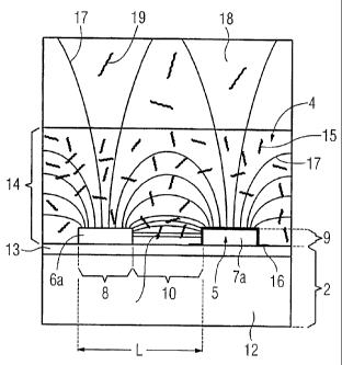
As shown in fig. 1, a biochip 1 comprises a flat carrier 2, on
one side of which a spot array 3 is applied. A
CA 02510719 2005-06-17
PCT/DE2003/004137
2002P06756WOUSWOCA
6 -
spot 4 contains immobilized catcher molecules, for example
oligonucleotides. If an analyte solution with unknown target
molecules is applied to a spot, then the target molecule is
coupled to the catcher molecule in the event of corresponding
matching in the base sequence. The property change brought
about by such a binding event, e.g. changes in the resistivity
or the dielectric constant, is detected impedance-
spectroscopically by means of an electrode arrangement 5.
A 2-pole electrode arrangement is present in the case of the
exemplary embodiment of fig. 2. This arrangement is applied to
the flat carrier 2 for example with the aid of a photolitho-
graphic method. The electrode arrangement 5 comprises two
electrodes 6, 7 designed in the form of an interdigital
structure. That is to say that each electrode comprises a
plurality of strip-type partial electrodes 6a, 7a which run
parallel to one another and in each case extend into the inter-
space between two partial electrodes of the respective other
electrodes. The partial electrodes 6a, 7a are connected to one
another by a likewise strip-type connecting conductor 6b, 7b
extending transversely with respect to the partial electrodes
6a, 7a. An AC voltage e.g. in the megahertz range is applied to
the electrodes 6, 7. The width 8 of the partial electrodes 6a,
7a is approximately 1 gm, their height 9 is approximately 100
to 500 nm. A spacing 10 of likewise approximately 1 4m is
present between the partial electrodes 6a, 7a.
The flat carrier 2 comprises a silicon layer 12 and an
insulating layer 13 e.g. made of silicon dioxide or silicon
nitride that is arranged between said silicon layer and the
electrodes 6, 7. The electrical interconnections and components
required for the impedance-spectroscopic measurement of binding
events are realized in a conventional manner by means of a
corresponding patterning of the silicon layer (not
illustrated). A reaction layer 14 made of a hydrogel is applied
CA 02510719 2005-06-17
PCT/DE2003/004137
2002P06756WOUSWOCA
7 -
on the insulating layer 13, which hydrogel is described in more
detail further below.
Catcher molecules 15 are embedded and homogeneously distributed
in the reaction layer 14 or the hydrogel, said catcher
molecules being illustrated symbolically and in overdimensioned
fashion in fig. 2. A catcher molecule with 300 bases has
approximately a length of 100 nm. Accordingly, a monomolecular
layer of catcher molecules in the case of conventional biochips
has at most approximately a thickness corresponding to the line
16 in fig. 2. It is readily apparent that such a layer can take
up relatively few catcher molecules 15 and, correspondingly,
can influence the electric field only to a small extent in the
case of binding events. By contrast, in the case of a biochip
according to the invention, the reaction region that contains
catcher molecules and is pervaded by field lines is
substantially extended and offers space for a number of target
molecules 15 that is greater by a plurality of powers of ten.
If an analyte solution 18 is applied to a spot array 3
configured in such a way or to a spot 4, then the target
molecules 19 contained in it, which is likewise illustrated
only symbolically and with exaggerated size in fig. 2, find a
substantially larger number of possible binding partners in the
form of the catcher molecules 15. The reaction layer 14 is
preferably dimensioned, or has a thickness, such that the
impedance-spectroscopic detection range is practically fully
utilized, which is achieved in any event given a thickness of
the reaction layer of approximately 2 to 100 m and is the case
in practice already at 2 - 10 m. Consequently, the binding-
specific measuring effect of the biochip can be substantially
increased given a corresponding concentration of catcher
molecules 15 in this region.
CA 02510719 2005-06-17
PCT/DE2003/004137
2002P06756WOUSWOCA
- 7a -
The reaction layer 14 is configured such that it provides an
aqueous reaction medium. Furthermore, it is configured such
that target molecules 19 or else other substances required for
a reaction, for example polymerase, can
CA 02510719 2005-06-17
PCT/DE2003/004137
2002P06756WOUSWOCA
- 8 -
indiffuse into it without its activity being impaired in the
process.
As already mentioned above, according to the invention a
hydrogel is used as the reaction layer 14. A hydrogel
represents an aqueous milieu in a mechanically stable form
whilst at the same time ensuring the substance exchange in a
predominantly aqueous environment. Through the choice of
chemical composition, which relates to the components and the
ratio thereof among one another, the properties of the
hydrogels such as water content, swelling behavior, mechanical
stability etc. can be varied over wide ranges.
A hydrogel that can be produced easily and has a good adhesion
both with respect to the electrode arrangement 5 and with
respect to the insulating layer 13 is an acrylamide-based
radical -cross 1inkable hydrogel containing a comonomer enabling
a covalent coupling of correspondingly modified catcher
molecules via linker groups. The hydrogel comprises, in
addition to the monomer precursor of polyacrylamide, a cross-
linking agent, at least one radical initiator, at least one
comonomer with reactive linker groups and, if appropriate, at
least one plasticizer. After layer production and subsequent
thermal crosslinking or photocrosslinking, a water-swellable
hydrogel is obtained containing reactive linker groups for the
immobilization of catcher molecules. Methylene bisacrylamide
and/or dimethylacrylates, for example tetraethylene glycol
dimethacrylate, are used as crosslinking agents.
The hydrogel mesh size can be set by varying the concentrations
of the crosslinking agent. The comonomer used contains maleic
anhydride and/or glycidyl (meth)acrylate. Mono-, di- and/or
triethylene glycol is suitable as plasticizer. The starting
substances mentioned are mixed with a polar, water-miscible
solvent, preferably with dimethylformamide.
CA 02510719 2005-06-17
PCT/DE2003/004137
2002P06756WOUSWOCA
9 -
The processing viscosity can be set by varying the proportion
of solvent. The adhesion to the flat carrier surface and also
to the electrode arrangement 5 can be reinforced by admixture
of customary adhesion promoters, for example silane-based
adhesion promoters.
Figs. 4 and 5 illustrate an exemplary embodiment with a 4-pole
electrode arrangement 20. The electrode arrangement 20 is
composed of two current electrodes 22, 23 and two voltage or
probe electrodes 24, 25. The current electrodes 22, 23 are
arranged and configured in accordance with the electrode
arrangement 5 of the exemplary embodiment according to fig. 2.
The probe electrodes 24, 25 are likewise strip-type and extend
as a meandering double strand through the interspaces present
between the partial electrodes 22a and 23a. A high-frequency AC
current is applied to the current electrodes 22, 23. A
voltmeter 26 is connected to the probe electrodes 24, 25 and
can be used to detect an alteration in the alternating electric
field on account of binding events.
The measurement can thus be effected independently of the
current electrodes, so that e.g. their polarization that
increases the electrode impedance cannot affect the
measurement. By contrast, in the case of a 2-pole electrode
arrangement, the electrode impedance has to be kept low by
means of a correspondingly high measurement frequency that is
unfavorable in terms of measurement technology, in order to be
able to determine the resistance of the analyte solution or of
the reaction layer, which resistance is crucial for the
measurement.
A 2-pole electrode arrangement in combination with very high
measurement frequencies (> 1 MHz) is advantageous for detecting
changes in capacitance within the reaction layer that are
caused by binding events.