Note: Descriptions are shown in the official language in which they were submitted.
CA 02511097 2005-06-17
WO 2004/080130 PCT/SE2004/000278
1
SCANNING-BASED DETECTION OF IONIZING RADIATION
FIELD OF THE INVENTION
The invention relates generally to apparatuses and methods for
scanning-based detection of radiation.
BACKGROUND OF THE INVENTION AND RELATED ART
Various line detectors for detecting ionizing radiation are
known in the art. While such detectors provide for instantaneous
one-dimensional imaging, two-dimensional imaging can only be
performed by means of scanning the line detector, and optionally
the radiation source, in a direction traverse to the one-
dimensional detector array. A one-dimensional image is typically
recorded each time the line detector, and optionally the
radiation source, has been moved a distance corresponding to the
width of the radiation sensitive area of the line detector.
Such scanning-based detection is time consuming and may be
impractical if large areas should be imaged. Movement of the
object being examined may occur during scanning, which could
severely reduce the image quality obtained. Thus, the scanning
should be made as fast as possible. The exposure, however, has
2o still to be selected such that the images possess high signal-
to-noise ratio and high dynamic range.
Furthermore, the spatial resolution is often an important
parameter. In many examinations it is desirable to obtain a
spatial resolution, which is better than 100 microns, e.g. as
good as 50 microns. This put very high demands on the detector
being used - both in terms of a narrow radiation sensitive area
and in terms of small readout elements or pixels. Alternatively
or additionally, very high requirements are put on the radiation
CA 02511097 2005-06-17
WO 2004/080130 PCT/SE2004/000278
2
source and any collimators employed in order to produce a very
thin planar beam of ionizing radiation. For instance, it is
extremely difficult - if at all possible - to produce a high
quality planar X-ray beam of a thickness of 50 microns and of a
modest intensity.
SZJNIMARY OF THE INVENTION
A main object of the invention is therefore to provide a
scanning-based ionizing radiation detecting apparatus and
method, which provide for measurement of extremely high spatial
resolution, but where the strong requirements on the detector
and the radiation source are relaxed.
In this respect there is a particular object to provide such an
apparatus and such a method, which are uncomplicated and can
produce high-quality two-dimensional images with excellent
signal-to-noise ratio, dynamic range, and image contrast.
A further object of the invention is to provide such an
apparatus and such a method, which enable a fast scanning across
the object to be examined.
A yet further object of the invention is to provide such an
apparatus and such a method, which are reliable, accurate, and
inexpensive.
These objects, among others, are attained by apparatuses and
methods as claimed in the appended claims.
The inventors have found that by providing a one-dimensional
detector unit with an ionizing radiation sensitive thickness,
which is larger than the thickness of a fan-shaped beam of
ionizing radiation which is exposed to the detector unit; and by
controlling the scanning by the one-dimensional detector unit to
CA 02511097 2005-06-17
WO 2004/080130 PCT/SE2004/000278
3
obtain a one-dimensional image of the fan-shaped beam of
ionizing radiation at every n'th length unit of the scanning,
where n is not lower than essentially half the thickness of the
fan-shaped beam in that length unit, but lower than the
thickness of the fan-shaped beam in the same length unit, a
scanning-based detection is achieved with high spatial
resolution in the two-dimensional image recorded without the
provision of extremely thin radiation beams, or extremely
narrow detectors.
The scanning step length n is preferably considerably lower
than the thickness of the fan-shaped beam, and more preferably
essentially half the thickness of the fan-shaped beam.
If the thickness of a fan-shaped beam is larger than the
radiation sensitive thickness of the one-dimensional detector
unit the scanning step length is set to a value smaller than
the radiation sensitive thickness of the one-dimensiona-1
detector unit, but not smaller than essentially half the
radiation sensitive thickness of the one-dimensional detector
unit.
The one-dimensional detector unit is preferably, but not
exclusively, a gaseous based parallel plate detector unit. Other
detector units that may be used include diode arrays,
scintillator based arrays, CCD arrays, TFT- and CMOS-based
detectors, liquid detectors, and solid-state detectors, e.g.
one-dimensional PIN-diode arrays with edge-on, near edge-on or
perpendicular incidence of X-rays.
Further characteristics of the invention, and advantages
thereof, will be evident from the detailed description of
preferred embodiments of the present invention given
30~ hereinafter and the accompanying Figs. 1-4, which are given by
CA 02511097 2005-06-17
WO 2004/080130 PCT/SE2004/000278
4
way of illustration only, and thus are not limitative of the
present invention.
BRIEF DESCRIPTION OF THE DRAWINGS
Fig. 1 illustrates schematically, in a side view, an apparatus
for scanning-based X-ray imaging according to a preferred
embodiment of the present invention.
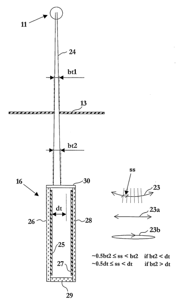
Fig. 2 is a schematic enlarged cross-sectional view of some of
the components of the apparatus of Fig. 1 taken along the line
A-A.
Fig. 3 is a schematic enlarged cross-sectional view of similar
components of a detector apparatus according to another
preferred embodiment of the invention.
Fig. 4 is a schematic enlarged cross-sectional view of similar
components of a detector apparatus according to yet another
preferred embodiment of the invention.
DESCRIPTION OF PREFERRED EMBODIMENTS
From top to bottom the apparatus in Fig. 1 comprises an X-ray
source 11, a filter device 12, a fan beam collimator 13, an
object table or holder 15, and a one-dimensional detector unit
16.
The X-ray source 11 is a conventional X-ray tube having a
cathode, which emits electrons, and an anode emitting X-rays
in response to being struck by the electrons, wherein the tube
has an operating voltage, which is the voltage drop between
the anode and the cathode, a tube current, which is the
current between the anode and the cathode, and a focal spot
size, which is the projected area in the direction of the
emitted X-rays of the anode, on which the electrons impinge
CA 02511097 2005-06-17
WO 2004/080130 PCT/SE2004/000278
(not explicitly illustrated). A typical focal spot dimension
is 0.1 - 1 mm. From such X-ray source it is difficult to
produce a high quality planar radiation beam of a thickness of
about 50 microns.
5 A filter device 12 is located just beneath the X-ray tube 11,
which typically includes thin metallic foils acting as filters
to absorb the lowest (and sometimes also the highest) energy
photons, which do not contribute significantly to the image
quality. The filter device may have variable spectral
transmission characteristics.
The fan beam collimator 13 may be a thin foil of e.g. tungsten
with a narrow radiation transparent slit etched away. The slit
is aligned with a corresponding line-shaped.sensitive area or
entrance slit of the detector unit 16 so that X-rays passing
through the slit of the fan beam collimator 13 will reach the
sensitive area or entrance slit of the detector unit 16. The
width of the slit is indicated by btl in Fig. 2. Since the
fan-shaped beam is divergent its thickness bt2 when reaching
the detector unit 16 is bigger (see Fig. 2 again). For a
distance from the X-ray tube 11 to the fan beam collimator 13
of about 45 cm, a distance from the X-ray tube 11 to the
detector unit 16 of about 65 cm, a focal spot size of 300 um
and a collimator slit width btl of about 70 microns, the beam
thickness bt2 at the detector unit 16 will be about 100
microns. The length of the slit is adapted so that the beam
has a beam width of suitable size, e.g. 30-50 mm, when
reaching the detector unit 16.
The detector unit 16 is illustrated in more detail in Fig. 2
and is oriented so that a planar or fan-shaped X-ray beam 24
can enter sideways between essentially planar cathode and anode
arrangements. Each of the electrode arrangements includes an
CA 02511097 2005-06-17
WO 2004/080130 PCT/SE2004/000278
6
electrically conducting electrode layer 25, 27 supported by a
respective dielectric substrate 26, 28, wherein the
arrangements are oriented such that the conductive cathode 25
and anode 27 layers are facing each other. A radiation
transparent window 30 is provided at the front end of the
detector unit to form an entrance for the fan-shaped beam 24
to the detector unit 16.
Preferably, the dielectric substrates 26, 28 and the window 30
define, together with a back end wall 29 and non-illustrated
sidewalls, a gas-tight confinement capable of being filled
with an ionizable gas or gas mixture. Alternatively, the
electrode arrangements are arranged within an external gas
tight casing (not illustrated). The ionizable gas or gas
mixture may e.g. comprise krypton and carbon dioxide or xenon
and carbon dioxide.
The detector unit 16 comprises further a readout arrangement
including a one-dimensional array of individual readout
elements (not explicitly illustrated) for recording a one-
dimensional image of the fan-shaped beam 2~.. Typically, the
readout arrangement is integrated with the anode arrangement.
The detector unit 16 may also comprise capabilities for
electron avalanche amplification in order to record very low
flux of X-rays, or detect each single X-ray with high
efficiency.
When avalanche amplification is used, the one-dimensional
detector unit 16 has a maximum ionizing radiation sensitive
thickness or height dt, i.e. a maximum thickness of a
radiation beam, which is contributing considerably to the
signals detected by the detector unit 16, which thickness or
height is typically smaller than the distance between the
conductive electrode layers 25, 27 (irrespective of the
CA 02511097 2005-06-17
WO 2004/080130 PCT/SE2004/000278
7
thickness bt2 of the fan-shaped beam when reaching the
detector unit 16). Thus, if the thickness bt2 of the fan-
shaped beam when reaching the detector unit 16 is less than
the thickness dt, the radiation sensitive thickness of the
beam as experienced by the detector unit 16 is bt2, whereas if
the thickness.bt2 of the fan-shaped beam when reaching the
detector unit 16 is larger than the thickness dt, the
radiation sensitive thickness of the beam as experienced by
the detector unit 16 is dt.
In one exemplary embodiment of the detector the distance
between the electrodes is 200-2000 microns, the radiation
sensitive thickness dt is 100-1500 microns, the depth (i.e.
length in the direction of the radiation beam 24) of the
detector is 10-100 mm, and the thickness (i.e. length
perpendicular to the plane of Fig. 2) of the detector is 20-
200 mm.
In an alternative version of the apparatus of Fig. 1, the
detector unit is replaced by a detector arrangement comprising
a plurality of one-dimensional detector units distributed in a
one- or two-dimensional array. The fan beam collimator 13 is
then replaced by a collimator with a plurality of narrow
radiation transparent slits - one for each detector unit. The
dimensions and orientations of the slits are such that each
detector unit is exposed to a respective fan-shaped X-ray
beam. By such version the scanning distance and time can be
considerably shortened.
For further details regarding different kind of gaseous-based
detector units for use in the present invention, reference is
made to the following U.S. Patents by Tom Francke et al. and
assigned to XCounter AB of Sweden, which patents are hereby
CA 02511097 2005-06-17
WO 2004/080130 PCT/SE2004/000278
8
incorporated by reference: Nos. 6,118,125; 6,373,065;
6,337,482; 6,385,282; 6,414,317; 6,476,397; and 6,477,223.
The X-ray tube 11, the fan beam collimator 13 and the detector
unit 16 are attached to a common E-arm 17, which in turn is
rotatably attached to a vertical stand 18 by means of a
spindle 19 approximately at the height of the X-ray tube 11.
In this manner, the X-ray tube 11, the fan beam collimator 13
and the detector unit 16 can be moved in a common pivoting
movement relative to an examination object arranged on the
object table 15 to scan the object and produce a two-
dimensional image thereof. The pivoting movement is
schematically indicated by arrow 23.
The object table 15 is firmly attached to a support 20, which
in turn is firmly attached to the vertical stand 18. For this
purpose the E-arm 17 is provided with a recess or similar in
the E-arm 17 (illustrated by the dashed lines). During
scanning, the object is kept still.
It shall be appreciated that the detector apparatus of Fig. 1
may be modified and arranged for linear movement of the X-ray
tube 11, the fan beam collimator 13 and the detector unit 16
with respect to the object being examined. Such linear
scanning movement is schematically indicated by arrow 23a in
Fig. 2. Yet alternatively, the fan beam collimator 13 and the
detector unit 16 may be rotated 16 in the horizontal plane
with respect to the object being examined as being
schematically indicated by arrow 23b in Fig. 2. Such
rotational-based scanning is disclosed in US Patent Nos.
6,067,342 (cordon) and 5,025,376 (Bona et al.), the contents
of which being hereby incorporated by reference.
CA 02511097 2005-06-17
' WO 2004/080130 PCT/SE2004/000278
9
It shall further be appreciated that the apparatus of Fig. 1
may be modified such that the object is moved during scanning,
while the X-ray tube 11, the fan beam collimator 13 and the
detector unit 16 are kept at rest.
Furthermore, the detector apparatus comprises a microprocessor
or computer 21 provided with suitable software for controlling
the apparatus and readout and post-processing of the signals
from the line detector unit 16 and a power supply 22 for
supplying the detector unit and the microprocessor or computer
21 with power and for driving a step motor or similar housed
in the vertical stand 18 for driving the spindle 19 and thus
the E-arm 17.
In operation, X-rays are emitted from the X-ray tube 11 and
pass through the filter device 12. ~nly X-rays passing through
the slit of the fan beam collimator 13 traverse the object. In
the object, the X-ray photons can be transmitted, absorbed or
scattered. The X-rays that are transmitted leave the object
and enter into the detector unit 16 and are detected. From the
detection a one-dimensional image of the object is formed.
During scanning, the E-arm 17, holding the X-ray source 11,
the fan beam collimator 13 and the detector unit 16, are moved
in a pivoting movement such that the detector unit scans
across the object in a direction, which is essentially
parallel with the object table 15. At regular movement
intervals, i.e. at moved distances ss, the detected signals
are read out and stored in a memory of the microprocessor 21.
When the X-ray source and the scanning are stopped, a number
of one-dimensional images of the object are formed and grouped
together by the microprocessor 21 to create a two-dimensional
image of the object.
CA 02511097 2005-06-17
' WO 2004/080130 PCT/SE2004/000278
In an alternative scanning technique the E-arm 17 is moved
relative the object stepwise, and the one-dimensional detector
unit 16 is detecting, while being still between the stepwise
movements.
5 Each scanning step has the length ss as indicated at the arrow
23 in Fig. 2. In the case as illustrated in Fig. 2 where the
one-dimensional detector unit 16 has an ionizing radiation
sensitive thickness dt, which is larger than the thickness bt2
of the fan-shaped beam 24 of ionizing radiation, the
10 microprocessor 21 is adapted, according to the present
invention, to control the detections by the one-dimensional
detector unit 16 during the scanning to obtain a one-
dimensional image of the fan-shaped beam 24 of ionizing
radiation at every n'th length unit ss of the movement, where
n is not lower than essentially half the thickness bt2 in that
length unit, but lower than the thickness bt2 in the same
length unit. In other words the scanning step ss can be
defined as
~0.5bt2 <_ ss < bt2 ~1>
provided that
bt2 < dt ~2~
Such provisions can assure a high spatial resolution in the
two-dimensional image.
Preferably, the scanning step ss is considerably lower than
the thickness bt2 of the fan-shaped beam 24 of ionizing
radiation in the length unit to improve the spatial resolution
in the two-dimensional image created from the number of one-
dimensional images formed from the scanning. An optimum
spatial resolution is obtained if the scanning step ss is
CA 02511097 2005-06-17
WO 2004/080130 PCT/SE2004/000278
11
essentially half the thickness bt2 of the fan-shaped beam 24
of ionizing radiation.
Given a beam thickness bt2 of about 100 microns, the scanning
step ss shall be lower, preferably considerably lower, than
100 microns, but not lower than about 50 microns. An optimum
spatial resolution is obtained for a scanning step ss of 50
microns.
If, however, the one-dimensional detector unit 16 used has an
ionizing radiation sensitive thickness dt, which is smaller
than the thickness bt2 of the fan-shaped beam 24 of ionizing
radiation (not illustrated), the microprocessor 21 is adapted,
according to the present invention, to control the detections
by the one-dimensional detector unit 16 during the scanning to
obtain a one-dimensional image of the fan-shaped beam 24 of
ionizing radiation at every i~th length unit ss of the
movement, where i is not lower than essentially half the
ionizing radiation sensitive thickness dt of the one-
dimensional detector unit 16 in the length unit, but lower
than the ionizing radiation sensitive thickness dt in the same
length unit. In other words the scanning step ss can be
defined as
-0.5dt 5 ss < dt (3)
provided that
bt2 > dt (4)
The scanning step is preferably considerably lower than the
radiation sensitive thickness dt, and more preferably
essentially about half the radiation sensitive thickness dt.
CA 02511097 2005-06-17
WO 2004/080130 PCT/SE2004/000278
12
In a preferred version of the present invention the scanning
step length ss is between about 0.5 and 0.8 times, preferably
between about 0.5 and 0.7 times, more preferably between about
0.5 and 0.6 times, and most preferably approximately 0.5
times, the thickness bt2 or the thickness/height/width dt,
whichever is smallest.
When the scanning step ss is reduced below the thickness bt2
or the thickness/height/width dt, whichever is smallest, the
spatial resolution is improved gradually (to the cost of
longer scanning times) until the scanning step ss is equal to
half the thickness bt2 or the thickness/height/width dt,
whichever is smallest. If the scanning step is further
reduced, no further improvement of the spatial resolution is
obtained.
It shall further be appreciated that while the detector unit
in the description above has been described as a gaseous-based
ionization detector, wherein the freed electrons are drifted
in a direction essentially perpendicular to the direction of
the incident ionization, the present invention is not limited
to such a detector. In fact, virtually any kind of detector
can be used in the present invention as long as it is a one-
dimensional detector capable of recording one-dimensional
images of ionizing radiation, to which it is exposed. Examples
of such detectors are scintillator-based detectors, PIN-diode
arrays, TFT (thin film transistor) arrays, CCD (charged
coupled device) arrays, CMOS circuits, or any other type of
semiconductor devices.
Fig. 3 is a schematic enlarged cross-sectional view similar to
the Fig. 2 cross-sectional view, but which illustrates a
detector apparatus based on a linear semiconductor array 16'.
The radiation sensitive thickness or width of the semiconductor
CA 02511097 2005-06-17
WO 2004/080130 PCT/SE2004/000278
13
array, i.e. dimension orthogonal to the extension of the
array, is indicated by dt. Note that this Figure illustrates
the case where the thickness bt2 of the planar radiation beam
24 at the entrance of the pin diode array is larger than the
linear semiconductor array width dt.
Fig. 4 is a schematic enlarged cross-sectional view similar to
the Figs. 2-3.cross-sectional views, but which illustrates a
detector apparatus based on a PIN-diode array 16 " . The
detector comprises a plate 31 of doped silicon carrying a
uniform metallic layer 25 " on one surface and a metallic
multiple strip layer 27 " on an opposite surface. The detector
apparatus is tilted with respect to the incident radiation beam
so that the beam impinges onto the uniform metallic Payer 25''
of the detector apparatus at an acute angle. Within the silicon
plate 31 the incident radiation interacts with the matter
whereupon electrons and holes are created. By applying a
suitable voltage over the metallic layers 25 " , 27 " the
electrons and holes are driven towards opposite surfaces of the
silicon plate 31, and either ones of the electrons or holes are
detected spatially resolved at the metallic multiple strip layer
27'°.
Note that Fig. 4 illustrates the case where the thickness bt2
of the planar radiation beam 24 at the entrance of the pin
diode array is smaller than the active PTN-diode array width
dt, which in turn depends on the depth of the PIN-diode array
and the tilting angle.
Optionally, a further collimator is arranged in front of the
detector (i.e. downstream of the object to be imaged), which
may define the ionizing radiation sensitive thickness dt.
CA 02511097 2005-06-17
WO 2004/080130 PCT/SE2004/000278
14
It shall yet further be appreciated that the present invention
is equally applicable for recording two-dimensional images of
radiation as scattered off an object, instead of being
transmitted there through.