Note: Descriptions are shown in the official language in which they were submitted.
CA 02511272 2005-06-30
1
SENSOR ARRAYS BASED ON ELECTRONIC OSCILLATORS
FIELD OF THE INVENTION
[0001] The present invention relates to an oscillator-based sensor
array.
BACKGROUND OF THE INVENTION
[0002] In-flight monitoring of gas turbine engines allows the
elaboration of adaptive maintenance plans. By periodically communicating
engine data to its service center, the aircraft operator benefits from
recommendations from maintenance experts. With additional sensors,
maintenance tasks can focus on specific vulnerable parts, rather than
reacting to the general behavior of the engine. Design engineers can also
anticipate specific problems before they happen, and start working on pre-
emptive design modifications. It is well recognized that development work
spreads over the useful life of an engine, as some unexpected durability
problems, often related to cyclic operation, arise only on aircraft wings.
[0003] For the aircraft operator, performance gains are expected
from better instrumentation associated with feedback control. Indeed, since
engines are currently designed with safety margins, to ensure durability in
all
conditions, some engines are not operated to the full capabilities of their
components. For example, knowing about the severity of the treatment
imposed to the most vulnerable turbine parts, it becomes possible to assess
the actual thrust capability of a particular engine. Throttle pushes, and
hence
increases in operating temperatures, can then be applied to healthier engines
without sacrificing safety. In addition to pure power gains, reductions in
fuel
consumption are also possible in the same way, as increasing operating
temperatures can improve engine cycle efficiency.
CA 02511272 2005-06-30
2
[0004] Furthermore, ground tests are expensive, accounting for
engine manufacturing, assembly and disassembly costs, and test cell
operation costs. Such expenses justify any push toward using as many
sensors as possible at one time. In order to validate analytical models,
engineers need more than post-testing observations of component
deterioration: they need temperature, pressure, and strain real-time
measurements, at every running condition of the tests. This detailed lower
level information allows to find the root flaws of models. Better monitoring
also offers the possibility of shorter tests, avoiding the necessity of
reaching
high deterioration levels to make useful observations. Experimental parts can
therefore be reused for multiple tests.
[0005] In instrumenting low access components such as the high
pressure turbine of an aircraft engine, lead routing represents a considerable
problem, with conventional sensing technology. Each thermocouple,
pressure sensor, or strain gauge generally requires a pair of wires to be
routed out to the data acquisition system, using a dedicated data transfer
slip-ring when installed on a rotating part. This leads to overcrowding of
communication lines in low access locations, and requires a large number of
data transfer slip-rings when monitoring rotating parts.
[0006] The gas turbine engine optimization process requires
considerable ground testing and flight experience, and despite all efforts
still
carries considerable safety margins. In this context, the industry would get
considerable benefits from better instrumenting the most vulnerable engine
components.
SUMMARY OF THE INVENTION
CA 02511272 2005-06-30
3
[0007] The present invention relates to a sensor array for
measuring various parameters in a machine environment. The sensor array
comprises a plurality of oscillators and an output onto which are multiplexed
the signals from each of the oscillators. Each of the oscillators includes a
feedback network having a natural frequency which varies with a parameters
to be measured, an amplifier which works in cooperation with the feedback
network to generate a signal that alternates at the natural frequency of the
feedback network and a limiter so configured as to limit the signal within a
predetermined range. The feedback network, the amplifier and the limiter
being interconnected in a loop.
[0008] The foregoing and other objects, advantages and features
of the present invention will become more apparent upon reading of the
following non restrictive description of an illustrative embodiment thereof,
given by way of example only with reference to the accompanying drawings.
BRIEF DESCRIPTION OF THE DRAWINGS
[0009) In the appended drawings:
[0010] Figure 1 is an illustration of the sensitive wire concept;
[0011] Figure 2 is a graph of a typical multiplexed signal obtained
from a sensor array;
[0012] Figure 3 is a schematic block diagram of the basic scheme
of operation of a single oscillator;
CA 02511272 2005-06-30
4
[0013] Figure 4 is a schematic block diagram of the oscillator
multiplexing principle based on addition of amplifier currents;
[0014] Figure 5 represents the circuit of a phase-shift oscillator;
[0015] Figure 6 represents the circuit of a parallel connection of
two phase-shift oscillators for multiplexing;
[0016] Figure 7 illustrates the circuit of a Wien bridge oscillator;
[0017] Figure 8 represents a graph showing the characteristics of
a diode signal clipper;
[0018] Figure 9 is a graph showing intrinsic carrier concentration;
[0019] Figure 10 represents the layout of a temperature sensitive
integrated circuit phase-shift oscillator generating a 67 kHz signal at room
temperature;
[0020] Figure 11 represents an integrated circuit capacitor top
view;
[0021] Figure 12 represents an integrated circuit capacitor cross
section;
[0022] Figure 13 represents an integrated circuit platinum resistor
top view;
CA 02511272 2005-06-30
[0023] Figure 14 is a graph showing calibration curves of the
sensitive wire of Figure 1 used as a platinum resistance temperature sensor;
[0024] Figure 15 represents the circuit of a parallel connection of
two Wien bridge oscillators for multiplexing;
[0025] Figure 16 is a graph showing the operation of a transistor
Q1 in the macroscopic high temperature Wien bridge oscillator of Figure 7, at
room temperature;
[0026] Figure 17 is a bode plot of a macroscopic high temperature
Wien bridge oscillator prototype, at room temperature, using handmade 600
pF capacitors, and 500 S2 resistors;
[0027] Figure 18 illustrates the waveform of a first macroscopic
high temperature oscillator prototype, measured at room temperature;
[0028] Figure 19 illustrates the waveform of a second macroscopic
high temperature oscillator prototype, measured at room temperature;
[0029] Figure 20 illustrates the waveform of the multiplexed
waveforms of Figures 18 and 19;
[0030] Figure 21 is a graph illustrating a frequency drift of two
multiplexed macroscopic high temperature oscillator prototypes at room
temperature;
CA 02511272 2005-06-30
6
[0031] Figure 22 is an elevational view of an oven setup for high
temperature macroscopic testing;
[0032] Figure 23 is a graph illustrating the behavior of
macroscopic high temperature oscillator prototypes when heated up and
cooled down in an oven, wherein two oscillators were multiplexed by current
addition but only one of the oscillator was heated up in the oven; and
[0033] Figure 24 is a graph showing the behavior of two
multiplexed macroscopic high temperature oscillator prototypes when heated
up in an oven.
DETAILED DESCRIPTION
[0034] The following disclosure presents in detail a sensor array
according to an illustrative embodiment of the present invention. Potential
applications will be presented thereafter, with an emphasis on high
temperature instrumentation for aircraft engines. However, it should be
understood that applications other than high temperature instrumentation for
aircraft engines are possible.
[0035] A new type of sensor array using emerging
microtechnologies is proposed for operation in machine environment. The
proposed sensor array is intended to measure distributions of various
parameters, like temperatures, pressures, strains, airflows, etc., in
transient
as in steady state, to enable ground testing, health monitoring and control of
low access machine components. The concept offers several advantages
over the existing measuring techniques. Specifically, it uses active
semiconductor devices to multiplex the signals of a number of sensors onto
CA 02511272 2005-06-30
7
the same leads. This avoids overcrowding of communication lines in low
access locations, and minimizes the number of required data transfer slip-
rings when monitoring rotating parts.
[0036] Various multiplexing strategies may be employed, e.g.
amplitude modulation (AM), frequency modulation (FM), or digital
multiplexing. For example, FM may be implemented in a sensor array, by
making the sensors generate waveforms by themselves, each within a
dedicated frequency band.
[0037] Using this concept, a common pair of leads may be used to
communicate the readings of a number of sensors using frequency
modulation. Each sensor is by itself an oscillator which generates a quasi-
sinusoidal signal maintained within one of the reserved frequency bands. The
frequency of each signal varies with the local parameter to be measured, but
stays within its reserved band. Advantageously, only one channel may be
used to acquire the multiplexed signal, and frequency analysis may then be
used to isolate the individual readings from one another.
[0038] Since the sensors of the sensor array are intended to be
very small, the resulting sensor array may be seen as a sensitive wire. Figure
1 shows a sensor array 100 having 10 sensors 102 to 1020, interconnected
by leads 122 and 124, with their respective assigned frequencies 112 to
1120. This sensor array 100 may be designed with various sensor spacing,
and various numbers of frequency bands, depending on the application.
Figure 2 shows the frequency domain multiplexed signal 110 resulting from
the combination of each of the individual sensors 102 to 102~o frequencies
112 to 1120.
CA 02511272 2005-06-30
8
[0039] Reserving a frequency band for each sensor limits the
possible number of sensors per sensor array. Another modulation approach
that may be used consists in allowing the frequency bands to overlap each
other, and to use temporal signal evolution to distinguish measurements from
one another. Using this approach, a larger number of sensors may be
integrated within a single array. One skilled in the art will understand that
more complex algorithms are required to treat the multiplexed signal in this
case.
[0040] At each measuring point (individual sensors 102 to 1020)
of the sensor array 100, various means may be employed to generate an
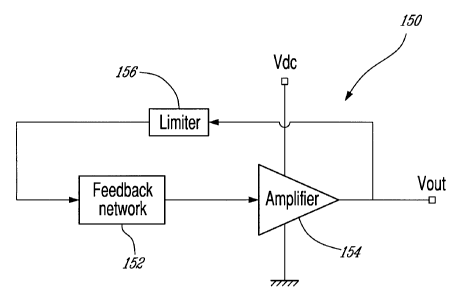
oscillating signal. The basic principle of the oscillator 150 used in the
illustrative embodiment of the present invention is schematized in Figure 3.
Three main components are used: a feedback network 152, an amplifier 154
and a limiter 156 which are all connected together in a loop configuration.
Around this loop, in order to produce an oscillation, the total gain is
greater
than unity, and the total signal phase shift corresponds to a finite number of
cycles. The limiter 156 is used to maintain the oscillator 150 within a
predetermined amplitude range, and hence to protect the looped components
from overloading. Without this limiter 156, the signal would be amplified
until
the amplifier 154 reaches saturation, or until one of the components fails.
[0041] The feedback network 152 may be any physical component
that reacts preferentially to different excitation frequencies, e.g. a
vibrating
beam or a quartz piezoelectric crystal characterized by a natural frequency,
or an electronic circuit. The frequency response of the network varying with
the parameter to be measured.
CA 02511272 2005-06-30
9
[0042] For example, the feedback network 152 may be a structure
whose natural frequency is influenced by temperature. This may be achieved
by using a mismatch in thermal expansion coefficients to make the structure
pre-stress level to vary with temperature. The pre-stress level influences the
frequency response of the structure, and, consequently, the frequency
response of the structure (the feedback network 152) depends on
temperature (the measured parameter). Pressure may be used in the same
way to change the frequency response of membranes, by pre-stressing
them, and the result is in this case a pressure-dependent feedback network.
[0043) The limiter 156 may either be mechanical, in the case of
vibrating devices, or electrical. For example, mechanical stoppers may limit
the displacements of vibrating structures, whereas diode bridges or heating
elements may limit voltages and currents, respectively. The limiter 156 may
operate on any component of the oscillator 150, or along any of its
connection lines. Its location is not limited to the one shown in Figure 3.
[0044] The amplifier 154 may be made of active electronic
components, and it is the power consumed by this amplifier 154 that is used
for multiplexing. Referring to Figure 4, a sensor array 180 including a
plurality
of individual oscillators (three shown) 150, 160 and 170 will be described.
[0045] When they are in operation, each amplifier 154, 164, 174
consumes a current that alternates at the frequency of the corresponding
oscillator 150, 160, 170 around a certain DC value. The currents for all of
the
individual oscillators 150, 160, 170 of the sensor array 180 are supplied
through the same two wires 182 and 184, which carry the frequency content
from each of the oscillators 150, 160, 170. Measuring the current through one
of these two leads 182, 184, and performing a frequency analysis, allows the
CA 02511272 2005-06-30
recuperation of the oscillating frequency of each of the individual
oscillators
150, 160, 170 of the sensor array 180. The current may be read, for example,
by measuring the voltage drop across resistor RM 186.
Detailed illustrative embodiment
[0046] The detailed non-restrictive illustrative embodiment
presented here uses only electronic components, for simplicity of integration.
Many types of electronic oscillators are available, e.g. RC and LC
oscillators,
negative resistance oscillators, multivibrators, etc. In the illustrative
embodiment, the following criteria were considered, in a non limitative
manner, in the selection of one type of electronic oscillator:
- inductors have not yet reached an acceptable level of miniaturization
in integrated circuits, and thus may be discarded from the oscillator
design, though further technological developments may change this
situation;
- in order to do efficient frequency modulation, the generated signal may
be advantageously as close as possible to a sinusoidal waveform;
- only the behavior of passive components of the feedback network 154
influence the oscillating frequency (for example, the temperature
sensitivity of active components, like transistors or diodes, does not
influence the oscillating frequency).
[0047] Based on those criteria, RC oscillators may be considered
as valuable candidates, and in particular phase-shift and Wien bridge
oscillators. Both these oscillators do not require inductors, and may generate
almost sinusoidal waveforms. Their oscillation frequencies are independent
CA 02511272 2005-06-30
11
from transistor or diode behavior and may be adjusted by changing resistor
or capacitor values only.
Phase-shift Oscillator
[0048] A phase-shift oscillator 210 used as an individual oscillator,
is schematized in Figure 5. It is composed of a high-pass feedback network
212, an amplifier 214 and a diode limner 216. Ideally, the amplifier 214
produces a signal phase shift of 180° that is independent of frequency.
The
feedback network 212 contains four high-pass filters 310, 320, 330, 340
connected in series that together provide an additional 180° phase-
shift at
one particular frequency. If the gain of the amplifier 214 is sufficiently
high to
compensate for the losses through the feedback network 212, at this
particular frequency, oscillation occurs. The oscillation frequency simply
corresponds to the frequency for which the feedback network 212 produces a
180° phase-shift, with the result of 360° total phase-shift
around the loop.
[0049] As shown in Figure 6, multiple phase-shift oscillators (only
two shown) 210 and 220 may be connected in parallel, and consequently add
their different current signals together. It is to be understood that the
configuration of Figure 6 with two oscillators is given as an example only and
that the number of oscillators is not limited to two. The currents from the
oscillators 210 and 220 of the sensor array 230 are all supplied through the
same two wires 232 and 234, which carry the frequency content from all the
oscillators 210, 220. Measuring the current through one of these two leads
232, 234 and performing a frequency analysis allows the recuperation of the
oscillating frequency of all of the individual oscillators 210, 220 of the
sensor
array 230. The current may read, for example, by measuring the voltage drop
across resistor RM 236.
CA 02511272 2005-06-30
12
Feedback Network
[0050] Since every elementary high-pass filter may provide a
phase-shift between 0 and 90°, at least three of those filters are used
in the
feedback network 212 in order to reach the required 180° shift. The
phase-
shifts are additive, such that three filters will produce a 0 to 270°
phase-shift,
and four filters, a 0 to 360° phase-shift. The advantage of using four
filters
instead of three is to obtain lower total losses. Using more filters would
lead
to even lower losses, but would become more cumbersome in an integrated
circuit, for a relatively negligible advantage in signal losses reduction.
[0051] Various means may be used to make the high-pass
feedback network 212 components depend on the measured parameters. On
the one hand, resistors 312, 322, 332 and 342 may be made of a
temperature-dependent material, like platinum, for temperature sensing.
They may also react to mechanical stresses, using the piezoresistance
effect, and be embedded in membranes for pressure sensing. On the other
hand, capacitances 314, 324, 334 and 344 are sensitive to the relative
spacing of their electrodes, and hence may be made to vary with
displacements of microstructures under accelerations. Those are only a few
non-limiting examples of how a RC feedback network 212 may be designed
to react to external stimuli.
Amplifier
[0052] Referring back to Figure 5, the amplifier 214 of the phase-
shift oscillator 210 provides a gain of at least 18.4, and a phase-shift of
180°
at the oscillating frequency. Since any amplifier gain gets lower at higher
temperatures, because of the reduction in transistor transconductance,
CA 02511272 2005-06-30
13
excess gain is provided at room temperature. This way, the oscillator 210
may be operable in the harsh environment of a typical machine.
[0053] Either MOSFETs or Bipolar transistors may be used in high
gain amplifiers. CMOS technology is also available with many types of
semiconductors, so that n-channel and p-channel MOSFETs may both be
used in the same integrated circuit. Several types of operational amplifiers
may also be used to provide the required high gains.
[0054] The phase-shift oscillator 210 of Figure 5 uses an amplifier
214 having an NMOS depletion load inverting high gain amplifier stage,
followed by a PMOS non-inverting low gain output stage. This is only one
example of an amplifier that may be used in the current application.
Wien Bridge Oscillator
[0055] A Wien bridge oscillator 410 is schematized in Figure 7. It
is composed of a Wien bridge 412, and two inverting amplifier stages 414a,
414b. At the oscillating frequency fo, the Wien bridge 412 gives a gain of
1/3,
and no phase-shift. Each amplifier stage 414a, 414b provides a 180°
phase-
shift, for a total phase-shift of 360° around the oscillator loop.
[0056] As a feedback network, the Wien bridge 412 has the
advantage that the oscillator 410 needs relatively low gain amplifier stages
414a, 414b considering the low losses through the Wien bridge 412 at the
oscillating frequency. A total gain of 3 needs to be provided by the two
amplifier stages 414a, 414b. Secondly, parasitic oscillation modes that may
appear due to undesired transistor behavior at high frequency are filtered out
by the Wien bridge 412.
CA 02511272 2005-06-30
14
[0057] The Wien bridge oscillator 410 may be used as a back-up
concept for the high gain amplifier 214 of the phase-shift oscillator 210 of
Figure 5. This new oscillator would use two low transconductance NMOS
transistors 421 and 422 only, as shown in Figure 7. The phase-shift oscillator
210 remains an advantageous concept because it provides a better quality of
signal, and consequently ease frequency modulation.
Limiter
(0058] In order to obtain a sinusoidal signal from any oscillator 150
of the general form shown Figure 3, the amplifier 154 gain is set to reach a
loop gain as close as possible to one. In the illustrative embodiment of the
present invention, since the amplifier 154 gain is affected by temperature, it
is
difficult to maintain a loop gain of one in every machine operating condition
unless some adjustments are continuously made to the amplifier 154 gain.
Such adjustments being unpractical, a limiter 156 is used as a control
feature, at the cost of slightly poorer signal quality. In most conditions,
the
amplifier 154 provides higher gain than really necessary, and the limiter 156
maintains the oscillator within stable operation.
[0059] Returning to Figure 7, in the Wien bridge oscillator 410, a
diode clipper 416 is used as a limiter 216 to limit the oscillating voltage
amplitude. The effect of the diode signal clipper 416 on the signal 430 is
shown in Figure 8, the signal 430 being clipped 432. Clipping a signal in this
way adds up harmonic frequency components above the main signal 430.
For effective frequency modulation, those components are filtered out as
much as possible.
CA 02511272 2005-06-30
[0060] Referring back to Figure 5, in the case of the phase-shift
oscillator 210, the feedback network 212 produces considerable losses,
which prevents harmonic components to survive near the main oscillating
frequency. In the case of the Wien bridge oscillator 410 shown in Figure 7,
however, the feedback network 412 (i.e. the Wien bridge), gives only poor
filtering close to the oscillating frequency, and the parasitic harmonic
components are conserved throughout the oscillator loop. Thus, another type
of limiter may be used with the Wien bridge oscillator 410, such as, for
example, a non-linear heating element (or lamp), to limit the signal without
affecting its shape. Such an element may be connected to limit the current
through one of the amplifier lines, as its resistivity increases under heat
generated by larger currents.
[0061] In order to get sinusoidal waveform generation without
using a cumbersome nonlinear heating element, the phase-shift oscillator
210 is preferred. Nevertheless, the Wien bridge oscillator 410 using a diode
clipper 416 as a limiter may be used to generate relatively clear sinusoidal
waveforms. As mentioned previously, the Wien bridge oscillator 410 is a
good back-up concept in situations where major problems are faced with the
phase-shift oscillator 410.
Wide Band Gap Semiconductors
[0062] Since the oscillator 150 shown in Figure 3 is designed to be
installed inside a machine, any electronic component present in the feedback
network 152, the amplifier 154 or the limiter 156 will be required to
withstand
the operating conditions of this machine. Amongst wide band gap
semiconductors that are available for operation at high temperature, silicon
carbide (SiC) and diamond represent good candidates.
CA 02511272 2005-06-30
16
Specific example: Integrated Circuit Development
[0063] In order to obtain the full advantages of the sensitive wire
100 shown in Figure 1, the feedback network 152, amplifier 154 and limiter
156 components of Figure 3 need to be miniaturized into an integrated circuit
such as, for example, the temperature sensitive integrated circuit phase-shift
oscillator 510 shown in Figure 10. It is to be noted that the oscillator 510
is
an illustrative example only.
Feedback Network
[0064] As discussed previously, many types of feedback networks
may be designed to be sensitive to many different machine parameters, such
as, for example, temperature, pressure, strain, vibrations, airflows, etc.
Referring to Figure 10, The temperature sensitive integrated circuit phase-
shift oscillator 510 will be described. The oscillator 510 includes a
temperature sensitive feedback network 512 using platinum resistors 522,
5222, 5223, 5224. It is the feedback network 212 of a phase-shift oscillator
210, as shown in Figure 5, and it constitutes the basis of a temperature
sensor array 230, shown in Figure 4, that may be installed in an engine.
[0065] In such an integrated temperature sensitive feedback
network 512, the platinum resistors 522, 5222, 5223, 5224 and capacitors
524, 5242, 5243, 5244 occupy a major portion of the substrate area 518 of
the temperature sensitive integrated circuit phase-shift oscillator 510. As
the
frequency to be generated by the oscillator 510 is reduced, the size of the
temperature sensitive feedback network 512 components increases. After
doing trade-offs to minimize the size of the lowest frequency temperature
sensitive feedback network 512, and fixing a limit to 1 mm2, 60 kHz was
CA 02511272 2005-06-30
17
found to be the lowest oscillating frequency at room temperature, with the
phase-shift oscillator 210 concept. Resistors 522, 5222, 5223, 5224 and
capacitors 524, 5242, 5243, 5244 of 200 pF and 10 kS2, respectively, may be
used in the temperature sensitive feedback network 512 to produce this
frequency. Microfabrication limitations of the clean rooms are used to
determine the smallest possible resistor cross section. Better resolution, and
hence lower frequency, may be achieved in the future, using high resolution
equipment. Lower oscillating frequency may also be achieved using the Wien
bridge oscillator 410 concept.
Capacitors
[0066] The capacitors 524, 5242, 5243, 5244 are composed of a
stack of layers 530, 5302, 5303 of conducting and dielectric materials, a top
view of which is shown in Figure 11 and a cross sectional view in Figure 12.
Si02 is used as the dielectric, whereas doped substrate SiC and polysilicon
act as electrodes. Conventional flat plate capacitors do not offer a
sufficiently
high capacitance to substrate area ratio. In order to reach 200 pF with
reasonable size capacitors, multiple layers of lateral flux capacitor
geometries are microfabricated. A combination of lateral and transversal
electric fields is used, in a configuration that may resemble the one
illustrated
in Figures 11 and 12. For the intent of the current implementation, a
capacitance increase factor of five is targeted over the flat plate capacitor
value. Hence,
C - ~o~'A ~ Equation 1
~d~er
Where
CA 02511272 2005-06-30
18
r~ is the multiplying factor taken as equal to five;
~ is the permittivity of free space;
s~, is the dielectric constant of Si02 (3.85);
A, is the covered substrate area; and
tde,, is the dielectric thickness between conducting
layers.
[0067] With r~ = 5 and tde; = 50 nm, a 200 pF square capacitor
uses up 242x242 pm of substrate area. A slightly different aspect ratio is
used in the layout of Figure 10, with the same area. It is to be understood
that the above described capacitor is given as an example only and that
other equivalent capacitors may be used as well.
Platinum Resistors
[0068] Considering the high electrical conductivity of platinum,
each resistor 522, 5222, 5223, 5224 of the temperature sensitive feedback
network 512 takes the shape of a long serpentine wire 540 with a small cross
section, as shown in Figure 13. The resistance of this serpentine wire 540 is
given by:
R = ~''L Equation 2
Acs
Where
pPt is the resistivity of pure platinum taken as 1.035 x
10-~ S2-m at 20 °C;
CA 02511272 2005-06-30
19
L, the total length of all serpentine wire 540 segments;
and
ASS, the cross section area of the serpentine wire 540.
[0069] The deposition thickness is taken as 100 nm, and the
lithography resolution, 2 ,um. Both the width 542 of the serpentine wire 540
segments and the spacing 544 between them are chosen to be 2 ,um, as
shown in Figure 13. For a square resistor of 10 kS2, 278 x 278 ,um of
substrate area is used. To minimize the parasitic inductance of this stack of
conducting serpentine wire 540 segments, the aspect ratio of the resistor is
properly chosen. An aspect ratio of four was arbitrarily used in the layout of
Figure 10, i.e. resistors 522, 5222, 5223, 5224.
[0070] In terms of microfabrication of the serpentine wire 540,
platinum may be deposited using physical vapor deposition (PVD), over a
Si02 insulating layer. Direct deposition over a SiC substrate could result in
film degradation at temperatures above 500 °C, due to formation of
platinum
silicides.
[0071] The power dissipated by each platinum resistor 522, 5222,
5223, 5224 causes self-heating. The first resistor 522 of the temperature
sensitive feedback network 512 is the one that dissipates the most power.
This resistor 522 may reach power peaks of less than 100 ~NV. In the event
that this resistor 512 suffers from overheating, it may need to be made of
wider platinum segments than the other resistors 5222, 5223, 5224. Any
configuration using multiple resistance values for the tour resistors 522,
5222, 5223, 5224 may also be investigated in terms of heat transfer.
Amplifier and Limiter
CA 02511272 2005-06-30
[0072] Referring back to Figure 10, the integrated circuit version of
the amplifier 214 and limiter 216 of Figure 3, amplifier 514 and limiter 516
respectively, use common technologies available in clean rooms, for example
ion implantation, oxide growth, and deposition. Various materials may need
to be used as MOSFET gate materials, to set threshold voltages to
acceptable levels. Amplifier 514 and limiter 516 resistors may be doped
directly into the semiconductor substrate 518, using ion implantation.
[0073] For the temperature sensitive integrated circuit phase-shift
oscillator 510 of Figure 10, the amplifier 514 and the limiter 516 are buried
underneath the platinum resistors 522, 5222, 5223, 5224, to save on
substrate 518 space. This may be done readily by depositing and polishing
an oxide layer onto the semiconductor components, before depositing the
platinum resistors 522, 5222, 5223, 5224.
Contacts
[0074] Electrical connections are made on a separate deposition
layer, over an oxide layer. Electronic components are reached through via
holes, using conventional etching technology. Ohmic contacts 526, 528 may
be made using materials recommended in the published literature.
Integration and Packaging
[0075) As illustrated in Figure 1, the resulting temperature
sensitive integrated circuit phase-shift oscillator array resembles a
sensitive
wire 100, with sensors 102 to 1020. Along the same two leads 122 and 124,
10 temperature sensitive integrated circuit phase-shift oscillators 510
(sensors 102 to 1020) are connected through their Ohmic contacts 526,
CA 02511272 2005-06-30
21
528. The leads 122 and 124, and the sensor 102 to 102~o circuits may all be
protected using an insulating material, like flexible ceramic or polymer
sheath, or rigid cement, depending on the application. The resulting sensor
array 100 is bonded to any substrate material using common sensor bonding
methods.
Array Design
[0076] Referring back again to Figure 10, by understanding the
behavior of the temperature sensitive feedback network 512, it is possible to
determine the calibration curve (frequency vs measured parameter) of the
temperature sensitive integrated circuit phase-shift oscillator 510, and hence
to appreciate its performance. In order to ease frequency modulation, the
designer of a sensor array 100 may want to make sure that every oscillator
510 keeps its signal within a dedicated frequency band, in all operating
conditions.
[0077] The example of a platinum resistor temperature sensor is
used again here to explain how to organize the multiple frequency bands of a
complete sensor array 100, using this approach of isolated frequency bands.
From experiments, in the range of 0 to 850 °C, the resistance of a
platinum
resistor is given by:
R = Ro ~1 + AT + BT Z ~ Equation 3
Where
A = 3.9083 x 10⁻³ °C-~; and
B = -5.775 x 10'' °C-2 [11 ].
CA 02511272 2005-06-30
22
[0078] Ro is the resistance at a reference temperature To of 0 °C.
This relation may be approximated by:
R ~ Ro ~1 + a~T -To ~~ Equation 4
Where
a is the average temperature coefficient, which
depends on reference To and on the temperature range
to be covered.
[0079] Each electronic oscillator of a sensing an-ay covers a
dedicated frequency range, for example the sensor array 100 shown in
Figure 1 covers the frequency range 110 starting at frequency 112 and
ending at frequency 1120, as illustrated in Figure 2. Within this range, each
sensor 102 to 102~o has a design frequency fd, at a design temperature Td.
Referring back to Figure 5, in the phase-shift oscillator 210 concept selected
here, the oscillating frequency is inversely proportional to R. Hence, for
each
sensor 102 to 1020:
f _ Rd ~ Ro ~1 + a~Td - To ~~
f~ R ~ Ro ~1 + a(T -To ~~ Equation 5
leading to:
1 + a~Td -To
f = fd Equation 6
1+a~T -To~
[0080] One way of spacing the sensors 102 to 10210 in the
frequency domain is to make consecutive sensors, for example sensors 102
and 1022, to have coincident oscillating frequencies when reaching
CA 02511272 2005-06-30
23
corresponding opposite temperature limits. Mathematically, if every sensor
102 to 102~o has the same design temperature Td, and the same operating
range dT,.ange~ this may be expressed by:
f T~ + OT2nge - f;-' Td _ OTZnge Equation 7
Using Equation 6, it follows that the ratio of two consecutive design
frequencies may be chosen from:
1+a Td + ~T2°ge -TO
fdi - Y _ Equation 8
fdi-1 1+a T -~Trange -T
0
[0081] The design frequencies then obey a geometric series of
ratio r, such that:
fd, = fd, - r~ ' Equation 9
(0082] As a consequence, if fd max is the maximum possible
frequency that may be generated, the number n of measuring points that may
be integrated to a sensor array 100 satisfies the following relation:
In 'f'' "~X
n < fd ' + 1 Equation 10
In r
[0083] The sensor array 100 of Figure 1 may be designed using
this methodology, with Td = 700 °C, dTlange = 300 °C, fd ~ = 30
kHz, fd maX =
CA 02511272 2005-06-30
24
600 kHz, and a = 3:85 x 10-3 °C. The resulting theoretical response
curves
are graphed in Figure 14. Once again, within the range of operation of the
sensor array 100, each oscillator 210 maintains itself within its dedicated
frequency band.
[0084] As mentioned previously, another valuable approach would
be to allow frequency bands to overlap each other, and to use temporal
signal evolution, or any other suitable methods, to distinguish measurements
from one another. More numerous sensors could be integrated in a single
array by using this second approach.
[0085] To appreciate the sensitivity of the sensor array 100,
Equation 6 needs to be differentiated with respect to T:
df ~ Equation 11
dT 1+a~T-To~
[0086] The ratio of the relative frequency variation to the
temperature variation is then given by:
a Equation 12
fOT 1+a~T-Tp
[0087] This ratio depends only on the measured temperature, and
is identical for every sensor 102 to 1020 of the sensor array 100. As
examples, at 400 and 800 °C, it is equal to -0.1 and -0.15 %/°C,
respectively.
[0088] The resolution of the sensor array 100 is in part limited by
the resolution of the frequency measuring system. Fundamentally, to improve
CA 02511272 2005-06-30
this resolution, the acquisition time is increased. The widths of the peaks,
in
the frequency domain, get narrower as the frequency analysis is performed
over a longer time interval. Tests conducted regarding the effect of signal
duration over frequency peak have suggested that if the FFT is conducted
over 200 periods, a frequency resolution better than 1 % may be expected.
For a sensor array 100 operating at 800 °C, this would mean a
temperature
resolution of less than 6.67 °C. This would satisfy the basic
requirements of a
gas turbine temperature sensor.
EXAMPLE
[0089] Referring to Figure 15, as a practical example of a sensor
array 630 according to the illustrative embodiment of the present invention,
in
which two high temperature macroscopic oscillators 610 and 620 are
connected so as to provide a multiplexed signal. The oscillators 610, 620
were built and operated in a high temperature environment, and as such high
temperature discrete components were assembled on two separate ceramic
substrates. The circuits were made to be sensitive to temperature, using
platinum resistors in the feedback networks 612, 622.
[0090] RF high power SiC MESFETs from Cree Inc. were used for
amplifying. Those transistors providing relatively low transconductance at low
power, the Wien bridge configuration 410, presented in Figure 7, was
selected for the oscillators 610, 620, because it allows for low gain
amplifier
stages. For oscillator 610, the Wien bridge feedback network 612 uses
1500 S2 resistors 712 (actually a 1000 S2 and a 500 S2 connected in series)
and 600pF capacitances 714, giving the oscillator an oscillating frequency of
215kHz. As for the oscillator 620, the Wien bridge feedback network 622
uses 1000SZ resistors 722 and 600pF capacitances 724, giving the oscillator
CA 02511272 2005-06-30
26
an oscillating frequency of 258kHz. It is to be understood that the stated
oscillation frequencies are at room temperature. The discrete components
were chosen or designed based on their resistance to high temperature, and
are listed in Table 1, using the identification symbols of Figure 7.
Component Symbol Supplier Part number or Value
description
Wien bridge R Omega A2132 50052
components A2142 1 OOOS2
C Handmade, 20mm 600pF
x 20mm stacking
of
5 0.004" thick
Pyrex ~ sheets
with 6 .062" thick
copper sheets
Transistors Q1, Q2 Cree CRF-22010-101 -
or
CRF-24010-101
MESFET
Amplifier resistorsRL Vishay DaleCL-4125DA 80052
RS Vishay DaleCL-4125DA 15052
Coupling filter CF - Same as Wien 600pF
components bridge capacitor
RF Huntington ALSR-5 25kSZ
Electric
Limiter resistorsRC Huntington ALSR-1 2pS~
Electric
Diodes - Cree CSD01060A -
Wire - - Steel AWG 21 -
Wire sheathing - Omega XC4-116 (Nextel -
440)
Connections - - Steel fasteners, -
aluminum terminals
Substrate - McMaster- 8489K54 (Macor) -
Carr
CA 02511272 2005-06-30
27
Power supply Vdc - - 80V
Table 1: List of oscillator discrete components
[0091] The basic amplifier stage 614a, 624a used in both circuits
610, 620, respectively, was numerically designed using the I-V
characteristics of the SiC transistor. In order to minimize the operating
voltages, the dissipated power, and hence heating of the components, the
Cree transistor was used in the triode region, very close to the threshold
voltage. Figure 16 shows the operating point of transistor Q1 over the
corresponding I-V curves. A standard curve tracer was used to measure the
transistor characteristics at room temperature. Parametric analysis was
performed by varying the values of amplifier resistors RS and RL, in order to
find an acceptable amplifier design.
[0092] The handmade 600 pF Pyrex-copper capacitors 714, 724
demonstrated sufficiently good behavior to keep bridge losses to an
acceptable level at the operating frequencies. Figure 17 shows the Bode plot
of a Wien bridge using those capacitors with 500 S2 resistors. Experimental
points illustrate that the resulting losses compare well with theoretical
calculations.
[0093] The room temperature signals of the two individual
oscillators 610 and 620, as well as their multiplexed signal, are plotted in
Figures 18, 19 and 20, respectively. A resistor RM 636 of 20 SZ was used to
measure the current going through the leads 632 and 634 carrying the total
current from the oscillators 610, 620, while the individual oscillator 610,
620
currents were obtained by feeding one oscillator at a time. The resistor RM
CA 02511272 2005-06-30
28
636 was connected in the 80 V power supply line 638, to limit its influence on
the behavior of the oscillators 610, 620.
[0094] The shapes and amplitudes of the two individual signals
may be understood by looking closely at the operation of the amplifiers 614a,
614b, 624a, 624b. For each oscillator 610, 620, two inverting amplifier stages
614a, 624a and 614b, 624b are fed with the same current carrying line. The
behavior of those two amplifier stages are quite different, in terms of
alternating signal. The alternating currents withdrawn by each of them are
different in magnitude and phase, and add up together to compose the
measured signal. The fact that the signal shows unsymmetrical waves (about
the y-axis) suggests that the two currents do not have a phase difference of
exactly 180°, as expected from theory. Furthermore, the current going
through the second amplifier stage 614a, 624a strongly depends on the Wien
bridge input impedance, which explains why the two oscillators 610, 620
show different output waveforms. Oscillator 610 uses a higher impedance
bridge, which causes the gain of the second stage to be higher. Hence, the
alternating current withdrawn by the second stage is more prominent in the
case of oscillator 610. This also explains why oscillator 610 produces a
higher amplitude signal than oscillator 620, even if the two oscillators 610,
620 use identical diode limiters 616, 626.
[0095] In the present concept, the sensor array 630 may be fed
with DC voltage only intermittently, depending on the desired temperature
measurement frequency. This minimizes power consumption and
overheating due to electric power dissipation. At every reading, real-time
frequency analysis is performed, using a fast fourier transform (FFT)
algorithm, and frequency peaks are detected and recorded. Data acquisition
is done over 200 periods of the lowest frequency signal of the sensor array
CA 02511272 2005-06-30
29
630, to ensure acceptable sensor sensitivity. The acquisition sampling
frequency corresponds to twice the frequency of the highest frequency
signal, to satisfy the Nyquist theorem. Using a dedicated FFT and peak
detection processor, a 1 Hz temperature measurement frequency may be
achievable.
[0096] The measuring sequence is described in Table 2, for a
measurement frequency of one measurement per 15 s.
Time (s) Operation
0 Power on
0.1 Data acquisition over Ot~,a
0.1 + ~t~aPower off
Frequency analysis
Peak detection
Data display and storage
15 Power on
Beginning of another sequence
Table 2 - Measuring sequence
[0097] The following results were obtained using the measuring
sequence just presented. Figure 21 shows how the frequencies of the two
multiplexed oscillators 610, 620 drift in time before stabilizing after about
ten
minutes. On the one hand, the drift of oscillator 610 may readily be explained
by the thermal inertia of the platinum resistors 712, 722. Those resistors
712,
722 are self-heating before reaching an equilibrium average temperature and
hence an average equilibrium resistance. This causes the frequency to
decrease asymptotically. On the other hand, the drift of oscillator 620 may be
CA 02511272 2005-06-30
due to progressive accumulation of charges in parasitic capacitances, for
example. In both cases, this initial frequency drift stays within 0.8% of the
stabilized frequency.
[0098] Referring to Figure 22, the two oscillators 610, 620 were
operated in an oven 800 up to a temperature of 180 °C. Temperature was
monitored inside the oven 800 using a standard thermocouple 810 located
under the oscillators 610, 620. In order to avoid direct radiation from the
resistive heating elements 820 onto the circuit components of the oscillators
610, 620, a steel case 830 was used as a shield. The thermocouple 810 and
the oscillators 610, 620 were all placed inside the steel shield 830, and are
assumed to have been kept within the same ambient temperature. Fiberglass
840 was used for electrical insulation only. Temperature was increased and
decreased at a maximum rate of 2 °C/min, which is believed to be slow
enough to ensure a good synchronization between oscillator 610, 620
temperature evolution and thermocouple 810 reading. Quasi-static conditions
were maintained throughout all operations.
[0099] Figure 23 shows the temperature response of oscillator 620
when it was operated for the first time. During this first operation, the
signals
of the two oscillators 610, 620 were multiplexed, but only oscillator 620 was
placed in the oven 800 and heated up. The results demonstrate that oscillator
610 was not influenced by the frequency variations of oscillator 620. The two
frequency signals were independent, as expected.
(00100] Hysteresis was observed when oscillator 610 was cooled
down back to room temperature. This is not believed to be due to thermal
inertia of the oscillator 610 circuit, considering the quasistatic character
of the
operation, but rather to some permanent modifications of electrical
CA 02511272 2005-06-30
31
properties. Oscillator 610 did not recover its exact original oscillating
frequency, even after 12 hours of rest at room temperature. It drifted from
256.1 kHz at the beginning of the operation to 250.5 kHz at the end of the
operation, for a 2% reduction in frequency.
[00101] Figure 24 shows the results of another operation where the
two oscillators 610, 620 were both placed in the oven 800 and heated up.
Oscillator 610 demonstrated a behavior that is closer to the theoretical curve
than oscillator 620. During this second operation, oscillator 620 experienced
a negligible permanent change in room temperature frequency, from 250.5
kHz at the beginning of the operation to 250.4 kHz at the end of the
operation. This suggests that, after a first stabilization anneal of an
oscillator,
hysteresis is reduced, and results may be repeatable.
[00102] During this second operation, above 170 °C, oscillator 620
stopped oscillating, whereas oscillator 610 oscillated up to about 184
°C.
Above those limits, transistor transconductance is too low, and the total loop
gain is smaller than unity, preventing oscillation. When the two oscillators
610, 620 were cooled down, oscillating signals came back.
Other Applications
[00103] Although high temperature applications have been
discussed, low temperature applications are not excluded. The conventional
silicon semiconductor technology may readily be used to build a low
temperature sensor array along the principle of the present invention, for
applications in biotechnological machines, for instance.
CA 02511272 2005-06-30
32
[00104] Fundamentally, any low access component operating in the
high temperature environment of a machine, and necessitating monitoring of
distributions of various parameters, like material temperature, fluid
temperature, fluid pressure and flow, or material strain, represents one
possible application of the present invention. Such applications may be found
in commercial or experimental products as well as in experimental
equipment.
[00105] Although the present invention has been described by way
of particular embodiments and examples thereof, it should be noted that it
will
be apparent to persons skilled in the art that modifications may be applied to
the present particular embodiment without departing from the scope of the
present invention.