Note: Descriptions are shown in the official language in which they were submitted.
CA 02511674 2012-04-19
130666
INTEGRATED MICRO OPTICAL BENCH WITH FLEXIBLE
DIELECTRIC SUBSTRATE
BACKGROUND OF THE INVENTION
This invention relates to integrated optics and, more specifically to an
integrated
micro optical bench for supporting an optoelectronic assembly.
Schemes incorporating a high number of discrete and integrated optical and
electronic
components are required to create optical systems in applications such as
server
backplanes, medical optical sensor arrays and general communications systems.
These systems create electrical and optical signals that require a high number
of
components and an even higher number of interconnections required for
generating
and controlling the signals and signal integrity desired in such products.
Traditional optical and electronic assembly use physical isolation in
individual
packages that add significant cost, materials, size and weight to the systems
they
serve. These isolated packages include hermetic metal and ceramic enclosures
that
prevent interaction with the environment or one another. Connectors and
interconnections between components add to reliability concerns. Separate heat
sinks
allow thermal isolation but create long physical paths that cause crosstalk
and EMI.
Optical interconnections require alignment and lens to account for more
physical
distance and additional amplification is required to account for losses due to
physical
distance and connectors. Complex hybrids created on silicon called silicon
optical
benches (SOB) attempt to solve this problem but are very limited in material
type,
matching characteristics, thickness and dielectric compatibility to microwave
and
optical requirements. Typically, such SOBs are used to pigtail rather than
integrate
many thousands of connections.
Thus, there is a continuing need in the prior art to achieve high signal
quality in both
electrical and optical interconnections in optoelectronic devices without
power
penalties by integrating their unique characteristics onto an integrated micro
optical
bench.
1
CA 02511674 2005-06-23
WO 2004/061506 PCT/US2003/038688
BRIEF DESCRIPTION OF THE INVENTION
A micro optical system as an integrated micro optical bench for supporting an
optoelectronic assembly comprises a rigid substrate and a thermal substrate
positioned
in a spaced relation from the rigid substrate. An optoelectronic integrated
circuit is
positioned on the rigid substrate generating an optical signal. A power
monitoring
unit is positioned on the rigid substrate and is in signal communication with
the
optoelectronic integrated circuit for monitoring at least a part of the
optical signal. A
thermistor is positioned on the rigid substrate for monitoring the temperature
of the
optical substrate. An electronic driver is positioned on the thermal substrate
for
driving the optoelectronic circuit and a control unit is also positioned
thereon. The
control unit is in signal communication with the power monitoring unit and the
thermistor for controlling the driver. At least one polymer substrate is
positioned so
as to overlay the electronic driver, the control unit, the power monitoring
unit, the
optoelectronic circuit and the thermistor. A plurality of patterned
metallization layers
are positioned on the at least one polymer substrate and electrically
interconnect the
electronic driver, the control unit, the power monitoring unit, the
optoelectronic
circuit and the thermistor.
This novel micro optical bench forms an integration platform that can be
applied to
many optoelectronically based systems such as charge coupled device (CCD)
sensor
array or photonic antenna for beamforming applications. The ability to co-
locate and
integrate high speed digital, mixed signal, analog, control and optoelectronic
circuits
made of optimal semiconductors is solved with the jointly integrated optical
and
electrical conductors, waveguides, and unguided wave interconnections of this
invention. Optical attenuation is reduced by ultra-close proximity integration
that
further avoids lenses as the capture angle, reduces angular misalignment,
reduces
extrinsic losses from imperfect joining.
The novel micro optical bench is described as a platform technology for
electrical and
optical interconnections, thermal, mechanical assembly and integration of
electronic,
optoelectronic, passive and active components is provided. This platform
provides
optical coupling and chip-to-chip interconnection by microwave electrical,
optical
2
CA 02511674 2005-06-23
WO 2004/061506 PCT/US2003/038688
guided and unguided waves, and power or bias electrical contacts or interfaces
by a
novel chip in flexible circuit, rigid or inflexible embodiments. The process
forms an
optically compliant wafer carrier, provides a method of assembly and
processing for
interconnection to electrical contacts and optical interfaces using unmounted
or
submounted bare components.
Provisions are made for close proximity coupling by free space, matching index
coupling material or guided means (fiber, waveguide) provided at the point of
light
emission or reception at the bare optical or optoelectronic component level,
using
deposition, integration, assembly or build-up to obtain co-planar, adjacent,
or directly
coupled mode propagation of light using the unique insulating electronic
material
dielectic.
Provision for copackaged and cojoined electrical control, feedback,
amplificaiton or
driving and bias circuits requiring electrical conductive interconnections are
provided
as integrated co-planar, microwave or bias tracks that employ the optical
material
media or insulation as a dielectric to the electrical conductor. A uniform
thermal
interface, management and isolation mechanism allows adjacent components to
independently operate in complete seclusion by dielectric insulation,
thermoelectric
cooler separation and segregation of micro-pipe circulation. The invention
illustrates
integration of Faraday isolation of unwanted electromagnetic inteference (EMI)
signals and optical interconnections between stages of typical circuit
architectures to
achieve high fidelity.
This invention specifically addresses achieving high signal quality in both
electrical
and optical interconnections without power penalties by integrating their
unique
characteristics required for high fidelity using a heterogeneous structure
within a
single platform. To achieve the desired bit error rate (BER) at low power
would
enable higher sensitivity and better integration with complimentary metal
oxide
semiconductor (CMOS).
BRIEF DESCRIPTION OF THE DRAWINGS
3
CA 02511674 2005-06-23
WO 2004/061506 PCT/US2003/038688
Figure 1 is a three dimensional view of an integrated micro optical bench for
supporting an optoelectronic circuit;
Figure 2 is a three dimensional view of individual elements of the integrated
micro
optical bench of Figure 1 as a transmitter;
Figure 3 is a top view of the integrated micro optical bench of Figure 1;
Figure 4 is a sectional view of the integrated micro optical bench of Figure
1;
Figure 5 is a sectional view of the integrated micro optical bench of Figure
1;
Figure '6 is a partial sectional view of integrated micro optical bench of
Figure 1;
Figure 7 is a sectional view of the integrated micro optical bench of Figure,
1;
Figure 8 is a view of a vertical. cavity surface emitting laser having an
annular
photodetector at the exit aperture of the laser;
Figure 9 is a partial view of the vertical cavity surface emitting laser with
annular
photodetector coupling light to a waveguide wherein the photodetector receives
light
from the waveguide;
Figure 10 is an end view of a vertical cavity surface emitting laser;
Figure 11 is a sectional view of the vertical cavity surface emitting laser of
Figure 9;
Figure 12 is a partial view of the integrated micro optical bench of Figure 1
including
a ball grid array and optical ball grid array in flip chip configuration;
Figure 13 is a partial view of the optical bench of Figure 1 including a ball
grid array
in flip chip configuration;
Figure 14 is a view of an optical ball grid array as a corner cube reflector;
Figure 15A is a view of an optical ball grid array as a flat mirror.
Figure 15B is a view of an optical ball grid array as a curved mirror;
4
CA 02511674 2005-06-23
WO 2004/061506 PCT/US2003/038688
Figure 16 is a schematic diagram of an integrated optoelectronic circuit for
modulating an optical signal;
Figure 17 is a cross sectional view of via holes in flexible dielectric
substrates;
Figure 18 is a cross sectional view of a vertical cavity surface emitting
laser with a
photo detector array and an abutting optical waveguide; and
Figure 19 is a cross sectional view of a vertical cavity surface emitting
laser with a
photo detector array and an abutting optical waveguide in a flip chip
configuration.
DETAILED DESCRIPTION OF THE INVENTION
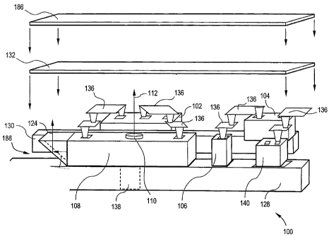
Referring to Figures 1, 2 and 3 a micro optical system as an integrated micro
optical
bench for supporting an optoelectronic assembly or circuit is shown generally
at 100.
The integrated micro optical bench 100 comprises a rigid substrate 128
comprising for
example an alumina ceramic or silicon substrate. A thermal substrate 130 is
positioned in a spaced relation from the rigid substrate 128. The rigid and
thermal
substrates 128, 130 are spaced apart at 188 by approximately 25 microns. The
space
designated by the reference numeral 188 may be left as a void space or may be
filled
with a flexible, thermally nonconducting filler material. An optoelectronic
integrated
circuit (OEIC) 108 is positioned on the rigid substrate 128 and may comprise
for
example a continuous wave or pulsed laser 114 providing an output optical
signal
124. The continuous wave (CW) or pulsed laser 114 includes for example a
distributed feedback (DFB) laser, a Fabry-Perot (FP) laser, a surface emitting
laser
such as a vertical cavity surface emitting (VCSEL) laser, an edge emitting
laser or
other suitable laser diode. It is contemplated that such laser includes front,
rear, side,
top and angled facet emission therefrom. The OEIC 108 may also include an
electroabsorptive modulator (EAM) 118 for modulating the output optical signal
124
of the laser 114. A power monitoring unit 106 (e.g. PIN photodiode, avalanche
photodiode - APD) is positioned on the rigid substrate 128. The power
monitoring
unit 106 is in signal communication at 116 with the optoelectronic integrated
circuit
108 by measuring the power of a segment of the output optical signal 116
radiated
from the rear facet of the laser 114 thus, monitoring the output performance
of the
CA 02511674 2005-06-23
WO 2004/061506 PCT/US2003/038688
optoelectronic circuit 108. A thermistor 140 is positioned on the rigid
substrate 128
for monitoring the temperature thereof.
As seen in Figure 3, the optoelectronic integrated circuit (OEIC) 108 provides
as out
put a pulsed or continuous wave optical signal 124 which may be directed to a
waveguide such as an optical fiber 184 (Fig. 5) or other optical devices. Also
in
Figure 3, it is seen that an electronic driver 102 provides as output three
drive signals,
122, 126, 252. Drive signal 122 is a DC bias signal for causing the laser 114
to
generate a continuous wave optical output signal 124. Alternatively drive
signal 122
(injection current) can be a direct modulation signal causing the OEIC 108 to
modulate between a light emitting diode (LED) state and a laser diode (LD)
state.
Drive signal 126 is a electrical signal to drive the electroabsorptive
modulator (EAM)
118. Drive signal 252 is an RF modulating signal to modulate an optical signal
in an
electro-optic modulator, (described below).
Continuing in Figures 1, 2 and 3, a microchip 180, including the electronic
driver 102,
such as a monolithic integrated circuit (MMIC) is positioned on the thermal
substrate
130. The electronic driver 102. provides drive signals 122, 126, 252 to the
optoelectronic circuit 108. A control unit 104, positioned on the thermal
substrate
130 and in signal communication at 194 with the power monitoring unit 106 and
at
192 with the thermistor 140, thereby controls the electronic driver 102. As
seen in
Figure 1, a plurality, of patterned metallization layers, or traces 136
electrically
interconnect the electronic driver 102 and the optoelectronic integrated
circuit 108.
The patterned metallization layers 136 also electrically interconnect the
power
monitoring unit 106 and the thermistor 140 and the control unit 104 and other
elements of the micro optical system 100. Still further, as seen in Figure 1
(and Figs.
4, 5, 6 7), a first flexible polymer substrate 132 is positioned so as to
overlay and
imbed therein the assembly of the electronic driver 102, the controller 104,
the power
monitoring unit 106, the optoelectronic integrated circuit 108, the thermistor
140, the
rigid and thermal substrates 128, 130 and the metallization layers 136 from
above, or
to underlay (e.g., to undergird) said assembly from below. Also as seen in
Figure 1
(and Figs. 4, 5, 6, 7), a second flexible polymer substrate 186 may be
provided.
6
CA 02511674 2005-06-23
WO 2004/061506 PCT/US2003/038688
Examples of suitable organic materials in the flexible polymer substrates 132,
186 and
the electro-optic modulator 146, 148 include poly(acrylates); poly(alkyl
methacrylates), for example poly(methyl methacrylate) (PMMA);
poly(tetrafluoroethylene) (PTFE); silicones; and mixtures comprising at least
one of
the foregoing organic materials, wherein the alkyl groups have from one to
about
twelve carbon atoms. The flexible polymer substrates 132, 186 may also
comprise for
example a polymer such as a polyimide polymer such as KAPTON . Coupled with
the fact that the rigid substrate 128 and the thermal substrate 130 are
separate
components displaced from one another, or joined by the flexible, thermally
nonconducting filler material, and the flexible nature of dielectric polymer
substrates
132, 186, the integrated micro optical bench 100 is capable of complete
flexure
between the rigid and thermal substrates 128, 130 and the components
positioned
thereon. This is seen in Figure 4.
As best understood from the description of the integrated micro optical bench
100, the
rigid substrate 128 provides a rigid platform for the precise alignment of
optical
components in the optoelectronic integrated circuit 108. The thermal substrate
130
provides a platform in the nature of a heat exchanger by and through which
heat,
generated by the control unit 104 and the electronic driver 102, may be
dissipated
from the integrated micro optical bench 100. To that end, thermal isolation
between
high heat energy generated by the electronic driver 102 and the stable
optoelectronics
is provided by the boundary 188 between the two physically adjacent substrates
128,
130. The electronic driver 102 and the OEIC 108 have separate thermal paths
enabled
by conduction such as by micropipes that change the direction of these
opposite
thermal paths.
Referring to Figure 4, the integrated micro optical bench 100 further
comprises a
polymer electro-optic device such as a waveguide 146, 148 positioned on or
imbedded within one of the flexible dielectric substrates 132, 186 and
receptive of the
optical signal 124 from the optoelectronic integrated circuit 108. The polymer
electro-optic waveguide 146, 148 may be for example, in the nature of a Mach-
Zehnder interferometer (MZI) as is shown in greater detail in Figure 16.
Therein, a
ground electrode 198 is positioned along one branch 212 of the MZI 146 and a
signal
7
CA 02511674 2005-06-23
WO 2004/061506 PCT/US2003/038688
electrode 142 is positioned along branch 212 opposite the ground electrode
198. The
signal electrode 142 is receptive of a modulating signal 252 from the
electronic driver
102 for modulating the optical signal 124 in the MZI 146. In Figure 16, the
MZI 146
comprises an input channel 208 receptive of the optical signal 124 from the
OEIC
108. A beam splitter 214 splits the optical signal 124 into two beams 254, 256
and
directs them separately along a first branch 210 and a second branch 212. In
the
embodiment of Figure 16, electrodes 142, 198 are positioned diametrically
opposed to
one another across one of the branches of the MZI 146. Alternatively, a
plurality of
ground electrodes 198 may be separately positioned along the first branch 210
and
second branch 212 with electrode 142 positioned between and along the first
branch
210 and the second branch 212.
Referring to Figures 3, 4, 5 and 7, the integrated micro optical bench 100
further
comprises an optical system 176 including at least one of a polarizer 134, for
polarizing the output optical signal 124, a collimator 150 for collimating the
output
optical signal 124, and a beam reflector 144 such as a prism or a mirror. The
optical
system 176 is receptive of the optical signal 124 from the optoelectronic
integrated
circuit 108 and operative thereby to condition or shape and direct the optical
signal
124 to the electro-optic waveguide 146, 148. The optical system 176 provides
corrective functions such as mode conversion, providing the correct reflective
angle
for coupling the output optical signal 124 to the MZI 146, 148 or to the
waveguide
184. As seen in Figures 5 and 6, the integrated micro optical bench 100 may
also
include an index matching polymer or glass 152 when the optical signal 124 is
coupled from the OEIC 108 (or the optical system 176) to waveguide 184 such as
an
optical fiber 184. Alternatively, no such index matching material may be
employed
and instead there may be a free space optical path between the OEIC 108 (or
the
optical systeml76) to the waveguide 184.
In Figures 8 - 14 and 18 and 19, the OEIC 108 includes a surface emitting
laser, such
as a vertical cavity surface emitting laser (VCSEL) 110. An annular
photodetector
154 is positioned around the exit aperture 168 of the VCSEL 110. In Figure 9,
the
VCSEL 110 provides as output an optical signal 112 directed to a waveguide 184
such as an optical fiber. In a test condition, for example, the photodetector
154 may
8
CA 02511674 2005-06-23
WO 2004/061506 PCT/US2003/038688
receive from the waveguide 184 a reflected return test signal 158 that
monitors the
operation of the VCSEL 110. Alternatively signal 158 may be a signal received
directly from the waveguide 184. In either case the micro optical system 100
is
operative thereby to act in a bi-directional manner (e.g., to transmit and to
receive).
In Figure 9, the first and second flexible dielectric substrates 132, 186
include via
holes 156, 178. Via hole 178 includes metallization layer 170 connected to
metallization layer 136. As seen in Figure 17, the micro optical system
includes the
plurality of via holes 156, 178. The first via hole. 156 is in the first
flexible dielectric
substrate 132 and the second via hole 178 is in the second flexible dielectric
substrate
186 aligned with the first via hole 156 along an axis 402. The first and
second via
holes 156, 178 are in the nature of a truncated cone subtending an angle of
theta
measured with respect to the axis 402. Typical values of theta lie in the
range of
approximately 25 degrees to 35 degrees. The first via hole 156 includes a
metallized
band (or layer) 408 on a surface thereof. The metallized band 408 includes a
plurality
of metallized bands on the surface 410 of the first via hole 156. The
plurality of
metallized bands 408, 410 include a nonmetallized band 406 positioned between
the
plurality of metallized bands 408, 410, thus making an alternating set of
metallized
and nonmetallized bands 406, 408, 410 wherein light 112 emanating from the
VCSEL
110 is prevented from leaking into the first dielectric substrate 132 while
light 174,
196 emanating from a waveguide or other device may pass through the
nonmetallized
band 406. Metallization is the deposition of thin film patterns of conductive
material
onto the dielectric substrates 132, 186, or the surfaces thereof, to provide
electrical
interconnections of electronic components of the .micro optical system. It
will be
understood that the metallized bands 408, 410 in the first via hole 156 do not
have an
electrical function.
In Figures 12, 13 and 19, the integrated micro optical bench 100 further
comprises a
ball grid array (BGA) 172 in a flip chip configuration for making direct
electrical and
mechanical connection between the rigid substrate 128 and the first and second
flexible dielectric polymer substrates 132, 186. In the flip chip
configuration the
OEIC 108 has all of its terminations on one side in the form of bump contacts
or bead
9
CA 02511674 2005-06-23
WO 2004/061506 PCT/US2003/038688
type pads to permit flip or face down mounting of the OEIC 108 by contact of
leads to
the required circuit interconnectors.
In addition, the integrated micro optical bench 100 further comprises an
optical ball
grid array (OBGA) 164 for coupling optical signals such as the output optical
signal
112 of the VCSEL 110, to other devices in the micro optical bench 100 or to
external
devices such as optical fiber 184. An Optical Ball Grid Array (OBGA) is a
structure
for coupling optoelectronic input/output (I/O) between optoelectronic devices
using
surface mount technology (SMT). In Figures 12, 13 and 19 an OBGA 164 comprises
an encapsulated volume which may encompass for example, free space, a
waveguide
(e.g., a polymer or Silica on silicon) or an optical media suitable for
carrying,
directing or guiding an optical ray (or signal). The OBGA 164 couples,
reflects, or
otherwise directs the output optical signal 112 from the VCSEL 110 to other
optical
or electronic devices in the micro optical bench 100. The OBGA 164 may be
shaped
as a ball or an ellipse, with top/bottom mounts or electrical bias pins to
power internal
microelectromechanical structures (MEMS), such as programmable deflection
surfaces (e.g., deformable mirrors under electronic control). The OBGA 164
forms an
interconnection protected from contamination and/or environmental effects
which is
also compliant so as to allow for the proper alignment of optical and
optoelectronic
devices of the micro optical bench 100. The OBGA 164 structure may involve a
portion of the optical rays impinging upon a reflective surface such as a flat
mirror
322 (Fig. 15A) or parabolic mirror 324 (Fig. 15B), or an intentionally
misaligned
micromachined corner cube retroreflector (CCR) 306 (Fig. 14) with an aperture
316
therein.
The deformable CCR embodiment (Fig. 14) of the OBGA 164 employs three
mutually orthogonal reflective surfaces or mirrors 310, 312, 314, forming a
concave
corner cube 306, to insure light 112 entering the OBGA 164 is at least
partially
reflected. An aperture 316 is optimized to permit a first portion of light 320
to pass
therethrough, with a second proportion of light 318 reflected by intentionally
deforming, or tilting, the CCR 306 by an electrostatic actuator. The first
facet 310 of
the CCR 306 may be at an angle of approximately60 to 75 degrees from
horizontal
and the second facet 312 at an angle of approximately 45 degrees. Other angles
CA 02511674 2005-06-23
WO 2004/061506 PCT/US2003/038688
provide reflections as required by the coupling surface exterior to the OBGA
164.
The aperture 316 permits reflection to be optimally selected for a
proportional energy
reflector having high efficiency and high energy pass-through effect. Photons
emanating from the facet, or impinging on the face, of an optoelectronic
device are
guided or directed by the OBGA 164 so as to enable low crosstalk and low
signal
attenuation along with highly accurate optical alignment.
In Figure 14 the OBGA is shown generally at 300. The OBGA 300 comprises an
adjustable (e.g. tiltable) CCR 306 encompassed within an index matched gel,
adhesive
or epoxy 308. The CCR 306 includes a set of mutually orthogonal facets 310,
312,
314. One facet includes an aperture 316. The CCR 306 is receptive of the light
112
emanating from the VCSEL 110. A first segment of the light output 320 passes
through the aperture 316 while.a second segment thereof 318 is reflected by
the facets
310, 312 to the photodetector 154. By tilting the CCR 306 at an angle of beta
the first
segment of light 320 can be passed through the aperture 316 while the
remaining
portion of the light signal 318 can be reflected to the detector 154. The
intended
operation of the OBGA 164 is to monitor optical signals or detect modulation
in
conjunction with separate or joint VCSEL/PIN devices 154, or with those
devices
otherwise co joined in a single device or in close proximity.
Deformable thermoplasticity or other deformable thermal effects, or deformable
mirror surfaces may comprise the CCR 306. Traditional ball grid array (BGA)
may
be micro-sized, forming chip-scale and wafer scale embodiments that merely
represent the microminiturization allowed under expected further improvements
in
lithography. Defonnability in MEMS structures, or other materials, involves
the
active bias or thermal activation of a material to induce an alteration in the
surface
profile. In this disclosure, by intentionally misaligning one or more of the
CCR
surfaces 310, 312; 314, one can provide a monitoring function of a proportion
of the
optical output signal 112 without the need to monitor 100% of the available
signal
strength. Static (set once) and dynamic adjustment of the OBGA 164 allows for
optical tuning over the lifecycle stresses induced by the environment or by
aging of
the micro optical bench 100.
11
CA 02511674 2005-06-23
WO 2004/061506 PCT/US2003/038688
Thus, based upon the foregoing description, a novel micro optical bench has
been
disclosed. Components thereof include an optical communications transceiver
function including laser diode based transmitter and photodiode receiver
placed upon
a novel platform optimized for high coupling ratio and low loss by aligning
the
mechanical optical axis and mode coupling with minimal material dispersion.
Modal
noise is suppressed by matching the mode field diameter and mode distribution
coupling in the applied media. Matching the electromagnetic waves reaching
devices
from optical or electrical connection is provided by a managed and colocated
dielectric and propagation media (optical core or conductor) to reduce mode
selective
loss effects. Proximity parameters impacting loss budget from devices and
structures
such as numerical aperture are also addressed by capturing the angular spread
of light
within the adjacent connection before it exceeds the core or detector
aperture.
Thermal isolation between high electrical driver heat energy and stable
optoelectronics is provided by a miniaturized boundary between two physically
adjacent substrates that have separate thermal paths enabled by conduction,
such as
micropipes that change the direction of these opposite thermal fronts. High
quality
electrical path matching is by overlay of controlled impedance paths. Low
connector
degradation is provided by coplanar direct metallization and minimized optical
return
loss by a polymer, air or other dielectric system encapsulating, radiating,
illuminating
or bridging these such interconnections with devices. Light emission from
devices or
structures that is orthogonal, perpendicular or at an odd angle to the device
or
coupling surface is coupled at minimal or zero dimension and loss by such
interconnection.
Any reference to first, second, etc., or front or back, right or left, top or
bottom, upper
or lower, horizontal or vertical, or any other phrase indicating the relative
position of
one object, quantity or variable with respect to another is, unless noted
otherwise,
intended for the convenience of description, and does not limit the present
invention
or its components to any one positional, spatial or temporal orientation. All
dimensions of the components in the attached Figures can vary with a potential
design
and the intended use of an embodiment without departing from the scope of the
invention.
12
CA 02511674 2005-06-23
WO 2004/061506 PCT/US2003/038688
While the invention has been described with reference to several embodiments
thereof, it will be understood by those skilled in the art that various
changes may be
made and equivalents maybe substituted for elements thereof without departing
from
the scope of the invention. In addition, many modifications may be made to
adapt a
particular situation or material to the teachings of the invention without
departing
from the essential scope thereof. Therefore, it is intended that the invention
not be
limited to the particular embodiments disclosed as the best mode contemplated
for
carrying out this invention, but that the invention will include all
embodiments falling
within the scope of the appended claims.
13