Note: Descriptions are shown in the official language in which they were submitted.
CA 02512165 2005-06-29
WO 2004/060676 PCT/US2003/041245
HEATER CHIP WITH DOPED DIAMOND-LIKE CARBON LAYER AND
OVERLYING CAVITATION LAYER
Field of the Invention
The present invention relates to inkjet printheads. In particular; it relates
to a
heater chip thereof having a doped diamond-like carbon layer above a resistor
layer.
More particularly, the doped diamond-like carbon layer includes silicon,
nitrogen,
titanium, tantalum or other and a cavitation layer of undoped diamond-like
carbon,
tantalum or titanium overlies the doped diamond-like carbon layer.
Bays-ound of the Invention
The art of printing images with inkjet technology is relatively well known. In
general, an image is produced by emitting ink drops from an inkjet printhead
at precise
moments such that they impact a print medium at a desired location. The
printhead is
supported by a movable print carriage within a device, such as an inkjet
printer, and is
caused to reciprocate relative to an advancing print medium. It emits ink
drops at times
pursuant to commands of a microprocessor or other controller. The timing of
the ink
drop emissions corresponds to a pattern of pixels of the image being printed.
Other than
printers, familiar devices incorporating inkjet technology include fax
machines, all-in-
ones, photo printers, and graphics plotters, to name a few.
Conventionally, a thermal inkjet printhead includes access to a local or
remote
supply of color or mono ink, a heater chip, a nozzle or orifice plate attached
to the heater
chip, and an input/output connector, such as a tape automated bond (TAB)
circuit, for
electrically connecting the heater chip to the printer during use. The heater
chip, in turn,
typically includes a plurality of thin film resistors or heaters fabricated by
deposition,
patterning and etching techniques on a substrate such as silicon. One or more
ink vias
cut or etched through a thickness of the silicon serve to fluidly connect the
supply of ink
to the individual heaters.
To print or emit a single drop of ink, an individual resistive heater is
uniquely
addressed with a small amount of current to rapidly heat a small volume of
ink. This
causes the ink to vaporize in a local ink chamber (between the heater and
nozzle plate)
and be ejected through and projected by the nozzle plate towards the print
medium.
1
CA 02512165 2005-06-29
WO 2004/060676 PCT/US2003/041245
Heretofore, conventional heater chip thin films on a silicon substrate
comprise
silicon nitride (SiN) and silicon carbide (SiC) overlying a resistor layer for
reasons
relating to passivation. Thereafter, a cavitation layer overlies the two
passivation layers
to protect the heater from corrosive ink and bubble collapse occurring in the
ink
chamber. In terms of thickness, the SiN is often 2000 to 3000 angstroms, the
SiC is
1000 to 1500 and the cavitation layer is 2000 to 4000 angstroms. Thus, at a
minimum,
the three combined layers above the resistor layer constitute a thickness of
several
thousand angstroms. Moreover, since all three layers have different chemical
compositions, no less than three processing steps are required.
Accordingly, the inkjet printhead arts desire optimum heater chip
configurations
requiring minimum processing steps without suffering a corresponding sacrifice
in
printhead function or performance.
Summary of the Invention
The above-mentioned and other problems become solved by applying the
principles and teachings associated with the hereinafter described inkjet
printhead heater
chip having a doped diamond-like carbon thin film layer and overlying
cavitation layer.
In one embodiment, a heater chip has a silicon substrate with a heater stack
formed of a plurality of thin film layers thereon for ejecting an ink drop
during use. The
thin film layers include: a thermal barrier layer on the silicon substrate; a
resistor layer
on the thermal barrier layer; a doped diamond-like carbon layer on the
resistor layer;
and a cavitation layer on the doped diamond-like carbon layer. Together, the
two doped
diamond-like carbon and cavitation layers serve the tri-functions of enhanced
adhesion,
passivation and protection from cavitation. The doped diamond-like carbon
layer
preferably includes silicon but may also include nitrogen, titanium, tantalum
or other.
When it includes silicon, a preferred silicon concentration is about 20 to 25
atomic
percent. More preferably, it is about 23 atomic percent. A preferred
cavitation layer
includes an undoped diamond-like carbon, tantalum or titanium layer. The doped
diamond-like carbon layer ranges in thickness from 500 to 3000 angstroms. The
cavitation layer ranges from 500 to 6000 angstroms. Thus, the combined
thicknesses
can range from as few as 1000 angstroms to 9000 angstroms.
In another aspect of the invention, the doped diamond-like carbon layer
becomes
formed on a substrate in a conventional PECVD chamber with a 200 to 1000 volt
bias
2
CA 02512165 2005-06-29
WO 2004/060676 PCT/US2003/041245
between the substrate and gas plasma. Preferably, the gas plasma includes
methane and
tetramethylsilane gasses.
In still another aspect, printheads containing the heater chip and printers
containing the printhead are disclosed.
These and other embodiments, aspects, advantages, and features of the present
invention will be set forth in the description which follows, and in part will
become
apparent to those of ordinary skill in the art by reference to the following
description of
the invention and referenced drawings or by practice of the invention. The
aspects,
advantages, and features of the invention are realized and attained by means
of the
instrumentalities, procedures, and combinations particularly pointed out in
the appended
claims.
Brief Description of the Drawings
Figure 1 is a perspective view in accordance with the teachings of the present
invention of an inkjet printhead having a heater chip with a doped diamond-
like carbon
and overlying cavitation layer;
Figure 2 is a perspective view in accordance with the teachings of the present
invention of an inkj et printer for containing the inkj et printhead;
Figure 3A is a perspective view in accordance with the teachings of the
present
invention of a heater stack of a heater chip having a doped diamond-like
carbon and
overlying cavitation layer; and
Figure 3B is a planar view in accordance with the teachings of the present
invention of a heater stack of a heater chip having a doped diamond-like
carbon and
overlying cavitation layer.
Detailed Description of the Preferred Embodiments
In the following detailed description of the preferred embodiments, reference
is
made to the accompanying drawings that form a part hereof, and in which is
shown by
way of illustration, specific embodiments in which the inventions may be
practiced.
These embodiments are described in sufficient detail to enable those skilled
in the art to
practice the invention, and it is to be understood that other embodiments may
be utilized
and that process, electrical or mechanical changes may be made without
departing from
the scope of the present invention. The term wafer or substrate used in this
specification
3
CA 02512165 2005-06-29
WO 2004/060676 PCT/US2003/041245
includes any base semiconductor structure such as silicon-on-sapphire (SOS)
technology, silicon-on-insulator (SOI) technology, thin film transistor (TFT)
technology, doped and undoped semiconductors, epitaxial layers of silicon
supported by
a base semiconductor structure, as well as other semiconductor structures well
known to
one skilled in the art. The following detailed description is, therefore, not
to be taken in
a limiting sense, and the scope of the present invention is defined only by
the appended
claims and their equivalents. In accordance with the present invention, we
hereinafter
describe an inkjet printhead heater chip having a doped diamond-like carbon
thin film
layer and an overlying cavitation layer.
With reference to Figure l, an inkjet printhead of the present invention is
shown
generally as 10. The printhead 10 has a housing 12 formed of any suitable
material for
holding ink. Its shape can vary and often depends upon the external device
that carries
or contains the printhead. The housing has at least one compartment 16
internal thereto
for holding an initial or refillable supply of ink. In one embodiment, the
compartment
has a single chamber and holds a supply of black ink, photo ink, cyan ink,
magenta ink
or yellow ink. In other embodiments, the compartment has multiple chambers and
contains three supplies of ink. Preferably, it includes cyan, magenta and
yellow ink. In
still other embodiments, the compartment contains plurals of black, photo,
cyan,
magenta or yellow ink. It will be appreciated, however, that while the
compartment 16
is shown as locally integrated within a housing 12 of the printhead, it may
alternatively
connect to a remote source of ink and receive supply from a tube, for example.
Adhered to one surface 18 of the housing 12 is a portion 19 of a flexible
circuit,
especially a tape automated bond (TAB) circuit 20. The other portion 21 of the
TAB
circuit 20 is adhered to another surface 22 of the housing. In this
embodiment, the two
surfaces 18, 22 are perpendicularly arranged to one another about an edge 23
of the
housing.
The TAB circuit 20 supports a plurality of input/output (I/O) connectors 24
thereon for electrically connecting a heater chip 25 to an external device,
such as a
printer, fax machine, copier, photo-printer, plotter, all-in-one, etc., during
use.
Pluralities of electrical conductors 26 exist on the TAB circuit 20 to
electrically connect
and short the I/O connectors 24 to the input terminals (bond pads 28) of the
heater chip
25 and those skilled in the art know various techniques for facilitating such
connections.
In a preferred embodiment, the TAB circuit is a polyimide material and the
electrical
4
CA 02512165 2005-06-29
WO 2004/060676 PCT/US2003/041245
conductors and connectors comprise copper. For simplicity, Figure 1 only shows
eight
I/O connectors 24, eight electrical conductors 26 and eight bond pads 28 but
present day
printheads have much larger quantities and any number is equally embraced
herein.
Still further, those skilled in the art should appreciate that while such
number of
connectors, conductors and bond pads equal one another, actual printheads may
have
unequal numbers.
The heater chip 25 contains at least one ink via 32 that fluidly connects to a
supply of ink internal to the housing. During printhead manufacturing, the
heater chip
25 preferably connects or attaches to the housing with any of a variety of
adhesives,
epoxies, etc. well known in the art. To form the vias, many processes are
known that
cut or etch the via through a thickness of the heater chip. Some of the more
preferred
processes include grit blasting or etching, such as wet, dry, reactive-ion-
etching, deep
reactive-ion-etching, or other. As shown, the heater chip contains four
columns (column
A- column D) of fluid firing elements or heaters. For simplicity in this
crowded figure,
four columns of six dots depict the heaters but in practice the heaters may
number
several hundred or thousand. Vertically adjacent ones of the fluid firing
elements may
or may not have a lateral spacing gap or stagger there between. In general,
however, the
fluid firing elements have vertical pitch spacing comparable to the dots-per-
inch
resolution of an attendant printer. Some examples include spacing of 1/300th,
1/600tn ,
1/1200x' , 1/2400 or other of an inch along the longitudinal extent of the
via. As
described below in greater detail, it will be appreciated that the individual
heaters of the
heater chip preferably become formed as a series of thin film layers made via
growth,
deposition, masking, patterning, photolithography and/or etching or other
processing
steps. A nozzle plate with pluralities of nozzle holes, not shown, adheres or
is
fabricated as another thin film layer such that the nozzle holes align with
and above the
heaters. During use, the nozzle holes project the ink towards a print medium.
With reference to Figure 2, an external device in the form of an inkjet
printer
contains the printhead 10 during use and is shown generally as 40. The printer
40
includes a carriage 42 having a plurality of slots 44 for containing one or
more
printheads 10. The carriage 42 reciprocates (in accordance with an output 59
of a
controller 57) along a shaft 48 above a print zone 46 by a motive force
supplied to a
drive belt 50 as is well known in the art. The reciprocation of the carriage
42 occurs
5
CA 02512165 2005-06-29
WO 2004/060676 PCT/US2003/041245
relative to a print medium, such as a sheet of paper 52 that advances in the
printer 40
along a paper path from an input tray 54, through the print zone 46, to an
output tray 56.
While in the print zone, the carriage 42 reciprocates in the 'Reciprocating
Direction generally perpendicularly to the paper 52 being advanced in the
Advance
Direction as shown by the arrows. Ink drops from compartment 16 (Figure 1) are
caused to be eject from the heater chip 25 at such times pursuant to commands
of a
printer microprocessor or other controller 57. The timing of the ink drop
emissions
corresponds to a pattern of pixels of the image being printed. Often times,
such patterns
become generated in devices electrically connected to the controller 57 (via
Ext. input)
that reside externally to the printer and include, but are not limited to, a
computer, a
scanner, a camera, a visual display unit, a personal data assistant, or other.
To print or emit a single drop of ink, the fluid firing elements (the dots in
columns A-D, Figure 1 ) are uniquely addressed with a small amount of current
to
rapidly heat a small volume of ink. This causes the ink to vaporize in a local
ink
chamber between the heater and the nozzle plate and eject through, and become
projected by, the nozzle plate towards the print medium. The fire pulse
required to emit
such ink drop may embody a single or a split firing pulse and is received at
the heater
chip on an input terminal (e.g., bond pad 28) from connections between the
bond pad
28, the electrical conductors 26, the I/O connectors 24 and controller 57.
Internal heater
chip wiring conveys the fire pulse from the input terminal to one or many of
the fluid
firing elements.
A control panel 58, having user selection interface 60, also accompanies many
printers as an input 62 to the controller 57 to provide additional printer
capabilities and
robustness.
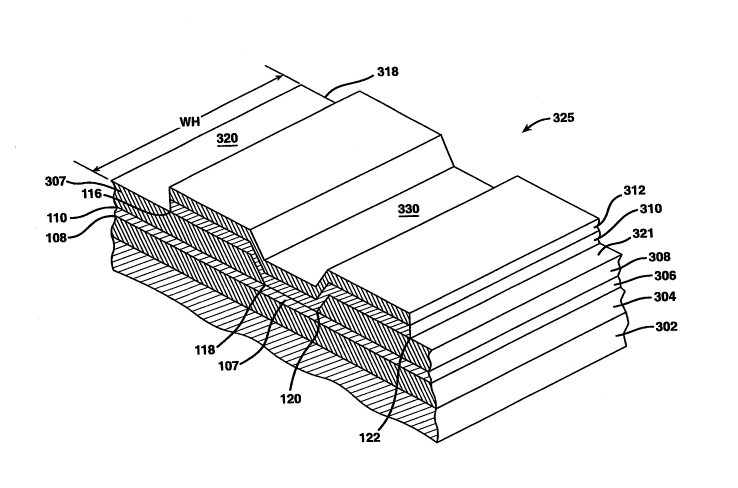
With reference to Figures 3A and 3B, appreciating the heater chip of the
present
invention is a substrate having been processed through a series of growth
layers,
deposition, masking, patterning, photolithography, andlor etching or other
processing
steps, a resulting heater chip 325 shown as a single heater stack 318 has a
multiplicity of
thin film layers stacked upon one another. Specifically, the thin film layers
include, but
are not limited to: a thermal barrier layer 304 on a substrate 302; a resistor
layer 306 on
the thermal barrier layer; a conductor layer (bifurcated into positive and
negative
electrode sections, i.e., anode 307, cathode 308) on the resistor layer to
heat the resistor
6
CA 02512165 2005-06-29
WO 2004/060676 PCT/US2003/041245
layer through thermal conductivity during use; a doped diamond-like carbon
layer 310
on the resistor layer; and a cavitation layer 312 on the doped diamond-like
carbon layer.
In various embodiments, the thin film layers become deposited by any variety
of
chemical vapor depositions (CVD), physical vapor depositions (PVD), epitaxy,
ion
beam deposition, evaporation, sputtering or other similarly known techniques.
Preferred
CVD techniques include low pressure (LP), atmospheric pressure (AP), plasma
enhanced (PE), high density plasma (HDP) or other. Preferred etching
techniques
include, but are not limited to, any variety of wet or dry etches, reactive
ion etches, deep
reactive ion etches, etc. Preferred photolithography steps include, but are
not limited to,
exposure to ultraviolet or x-ray light sources, or other, and photomasking
includes
photomasking islands and/or photomasking holes. The particular embodiment,
island or
hole, depends upon whether the configuration of the mask is a clear-field or
dark-field
mask as those terms as well understood in the art.
As is apparent from Figures 3A and 3B, the substrate 302 provides the base
layer
upon which all other layers are formed. In one embodiment, it comprises a
silicon wafer
of p-type, 100 orientation, having a resistivity of 5-20 ohm/cm. Its beginning
thickness
is preferably, but not necessarily required, any one of 525 +/- 20 microns,
625 +/- 20
microns, or 625 +/- 15 microns with respective wafer diameters of 100 +/- 0.50
mm, 125
+/- 0.50 mm, and 150 +/- 0.50 mm.
The next layer is a thermal barrier layer 304. Some embodiments of the layer
include a silicon oxide layer mixed with a glass such as BPSG, PSG or PSOG
with an
exemplary thickness of about 1 to about 3 microns, especially 1.82 +/- 0.15
microns.
This layer can be a grown layer as well as a deposited one.
Subsequent to the thermal barrier layer and disposed on a surface thereof is
the
heater or resistor layer 306. Preferably, the resistor layer is about a 50-50%
tantalum-
aluminum composition layer of about 1000 angstroms thick. In other
embodiments, the
resistor layer includes essentially pure or composition layers of any of the
following:
hafnium, Hf, tantalum, Ta, titanium, Ti, tungsten, W, hafnium-diboride, HfB2,
Tantalum-nitride, Ta2N, TaAI(N,O), TaAlSi, TaSiC, TalTaAI layered resistor,
Ti(N,O)
and WSi(O).
A conductor layer overlies a portion of the resistor layer 306 (e.g., that
portion of
the resistor layer excluding the portion between points 118 and 120) and
includes an
anode 307 and cathode 308. In one embodiment, the conductor layer is about a
99.5 -
7
CA 02512165 2005-06-29
WO 2004/060676 PCT/US2003/041245
0.5% aluminum-copper composition of about 5000 +/- 10% angstroms thick. In
other
embodiments, the conductor layer includes pure or compositions of aluminum
with 2%
copper and aluminum with 4% copper.
On a surface of the resistor layer 306 between the anode and cathode (as
between points 118 and 120) is a distance that defines a heater length LH. In
an area
107 generally beneath the heater length, the resistor layer 306 has a
thickness ranging
from a surface 108 to a surface 110 that defines a resistor thickness. A width
of the
resistor layer 306 also defines a heater width, WH, as shown. As taught in co-
pending
Lexmark application Serial No.lO/146,578, having a filing date of May 14,
2002, titled
"Heater Chip Configuration for an Inkjet Printhead and Printer" and expressly
incorporated herein by reference, the energy required to stably j et ink from
an individual
heater 318 is a function of heater area (heater width, WH, multiplied by
heater length,
LH) and thickness TH or heater volume. While the heater shape is generally
depicted as
having a square or rectangular shape, it is understood that other, more
complex shapes
may be used that are not described simply by a width WH and a length LH.
However
complex the heater shapes may be, they still have an area AH. The heater area
AH is
formed by the portion of the resistor layer 306 that is bounded between the
anode 307
and the cathode 308. As a representative example, the invention contemplates
jetting
ink from a single heater with an energy/volume of about 3 to about 4 GJ/m3.
More
particularly, it is about 2.94 to about 3.97 GJ/m3. In turn, the power/volume
is greater
than about 1.5 watts/m3. To produce 2 ng ink drops, the invention contemplates
a heater
area of about 300 micronsa while 30 ng ink drops correspond to a heater area
of about
1000 microns2.
On a surface portion of the resistor layer 306, as between points 118 and 120,
and along upper surface portions 320, 321 of the conductor layer, as between
points 116
and 118 and between points 120 and 122, is a doped diamond-like carbon layer
310. In
one embodiment, the doped diamond-like carbon layer ranges essentially
uniformly in
thickness from about 500 to about 3000 angstroms +/- about 10%. In another
embodiment, the thickness is as large as about 8000 angstroms.
The dopant of the doped diamond-like carbon layer preferably includes silicon
but may also include nitrogen, titanium, tantalum, a dielectric or other. When
it
includes silicon, a preferred silicon concentration is about 20 to 25 atomic
percent.
More preferably, it is about 23 atomic percent.
8
CA 02512165 2005-06-29
WO 2004/060676 PCT/US2003/041245
Among other things, it has been discovered that a single doped diamond-like
carbon layer above the heater layer provides excellent passivation properties
as
compared to conventional heater chips with two passivation layers. Use of a
single
layer simplifies the manufacturing processing by eliminating a deposition step
from the
process flow and also improves process capability. It also exhibits enhanced
adhesion
to the underlying layer as compared to essentially pure diamond-like carbon. A
description of a pure diamond-like carbon layer on a resistor layer can be
found in
Lexmark-assigned, co-pending application, Serial No. 10/165,534, filed June 7,
2002,
titled "Energy Efficient Heater Stack Using DLC Island" which disclosure is
incorporated herein by reference.
Unfortunately, a single layer of doped diamond-like carbon does not
sufficiently
withstand the corrosive effects of ink or the long-term bubble collapse
effects in the area
330 generally above the heater. Thus, to improve longevity, a cavitation layer
312 is
disposed on an upper surface of the doped diamond-like carbon layer. Together
the two
doped diamond-like carbon and cavitation layers serve the tri-functions of
enhanced
adhesion, passivation and cavitation.
In a preferred embodiment, the cavitation layer includes an undoped diamond-
like carbon, pure or doped tantalum, pure or doped titanium or other layer. In
another
embodiment, the cavitation layer ranges essentially uniformly in thickness
from about
500 to about 6000 angstroms. In turn, the combined thicknesses of the doped
diamond-
like carbon layer and the cavitation layer ranges from as few as 1000
angstroms to 9000
angstroms. Actual thicknesses, however, depends upon application.
A nozzle plate, not shown, is eventually attached to the foregoing described
heater stack to direct and project ink drops, formed as bubbles in the ink
chamber area
330 generally above the heater, onto a print medium during use.
In another aspect of the invention, the doped diamond-like carbon layer
becomes
formed on the substrate 302 in a conventional PECVD chamber with about a 200
to
about 1000 volt bias between the substrate and gas plasma. Preferably, the gas
plasma
includes methane and tetramethylsilane gasses. Thereafter, in the event the
cavitation
layer is an undoped diamond-like carbon layer, the flow of tetramethylsilane
gas to the
chamber can be shut off thereby allowing pure diamond-like carbon to plate or
build up.
This saves processing steps.
9
CA 02512165 2005-06-29
WO 2004/060676 PCT/US2003/041245
In other embodiments, the diamond-like carbon layer is deposited at a pressure
of about 30 mtorr using a power density of about 30 to 35 KW/m2 with a
deposition rate
of about 1000 to 2000 angstroms/minute.
Finally, the foregoing description is presented for purposes of illustration
and
description of the various aspects of the invention. The descriptions are not
intended,
however, to be exhaustive or to limit the invention to the precise form
disclosed.
Accordingly, the embodiments described above were chosen to provide the best
illustration of the principles of the invention and its practical application
to thereby
enable one of ordinary skill in the art to utilize the invention in various
embodiments
and with various modifications as are suited to the particular use
contemplated. All such
modifications and variations axe within the scope of the invention as
determined by the
appended claims when interpreted in accordance with the breadth to which they
are
fairly, legally and equitably entitled.