Note: Descriptions are shown in the official language in which they were submitted.
CA 02512449 2005-07-19
BALLAST WITH FILAMENT HEATING CONTROL CIRCUIT
Statement of Related Annlications
The present application claims priority to U.S. provisional patent
application Serial No. 60/639,422 (titled "Generating filament voltage during
dimming with filament cut-off feature during full light level for electronic
ballast," filed on December 27, 2004), the disclosure of which is incorporated
herein by reference.
The subject matter of the present application is related to that of U.S.
patent application Serial No. 11/010,845 (titled "Two Light Level Ballast,"
filed
on December 13, 2004, and assigned to the same assignee as the present
invention), the disclosure of which is incorporated herein by reference.
Field of the Invention
The present invention relates to the general subject of circuits for
powering discharge lamps. More particularly, the present invention relates to
a
ballast that includes a filament heating control circuit.
Background of the Invention
Ballasts for gas discharge lamps are often classified into two groups
according to how the lamps are ignited - preheat and instant start. In preheat
ballasts, the lamp filaments are preheated at a relatively high level (e.g., 7
volts
peak) for a limited period of time (e.g., one second or less) before a
moderately
high voltage (e.g., 500 volts peak) is applied across the lamp in order to
ignite
the lamp. In instant start ballasts, the lamp filaments are not preheated, so
a
higher starting voltage (e.g., 1000 volts peak) is required in order to ignite
the
lamp. It is generally acknowledged that instant start operation offers certain
advantages, such as the ability to ignite the lamp at a lower ambient
temperatures and greater energy efficiency (i.e., light output per watt) due
to no
expenditure of power on filament heating during normal operation of the lamp.
On the other hand, instant start operation usually results in considerably
lower
lamp life than preheat operation.
CA 02512449 2005-07-19
2
Because a substantial amount of power is unnecessarily expended on
heating the lamp filaments during normal operation of the lamp, it is
desirable to
have preheat-type ballasts in which filament power is minimized or eliminated
once the lamp has ignited. Ballasts that provide filament preheating prior to
lamp ignition, but that cease to provide filament heating after the lamp
ignites,
are commonly referred to as programmed start ballasts.
When a lamp is operated at a current level that approaches the rated
normal operating current of the lamp (e.g., about 180 milliamperes rms for a
T8
lamp), the absence of filament heating has little negative impact upon the
useful
operating life of the lamp. Thus, ordinary programmed start ballasts work well
with lamps that are driven at a normal (i.e., full-light) level. Conversely,
when a
lamp is operated at a current level that is substantially less than the rated
normal
operating current of the lamp (i.e., such as what occurs when the lamp is
operated in a dimmed mode), the absence of filament heating has been observed
to have a considerable negative impact upon the useful operating life of the
lamp. Thus, ordinary programmed start ballasts are not well suited for driving
lamps at substantially reduced light levels.
Therefore, a need exists for a ballast that primarily operates in a
programmed start manner (i.e., that provides filament heating prior to lamp
ignition, and then no filament heating during full-light operation of the
lamp),
but that has an added feature of providing filament heating during dimmed
operation of the lamp. Such a ballast would represent a significant advance
over
the prior art.
Brief Description of the Drawings
FIG. 1 is a block diagram schematic of an electronic ballast with a
filament heating control circuit, in accordance with a preferred embodiment of
the present invention.
FIG. 2 is a detailed electrical schematic of an electronic ballast with a
filament heating control circuit, in accordance with a preferred embodiment of
the present invention.
CA 02512449 2005-07-19
3
Detailed Description of the Preferred Embodiments
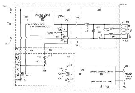
Fig. 1 describes an electronic ballast 10 for powering at least one gas
discharge lamp 20 having first and second lamp filaments 22.24 is described in
FIG. 1. Ballast 10 comprises an inverter 200, an output circuit 300, a
filament
heating control circuit 400, and a dimming control circuit 500.
Inverter 200 has first and second input terminals 202,204, and first and
second output terminals 206,208. Input terminals 202,204 are adapted to
receive
a source of substantially direct current (DC) voltage, V~~~, such as that
which is
commonly provided by a combination of a full-wave rectifier and boost
converter that receive a conventional source of alternating current (AC)
voltage
(not shown), such as 120 volts rms at 60 hertz. During operation, inverter 200
preferably provides an alternating voltage between output terminals 206,208;
preferably, the alternating voltage has a high fi-eduency (i.e., 20,000 hertz
or
greater).
Output circuit 300 is coupled to inverter output terminals 206,208, and
includes first, second, third, and fourth output connections 302,304,306,308
adapted for connection to lamp 20. More specifically, first and second output
connections 302,304 are adapted for connection to l7rst lamp filament 22,
while
third and fourth output connections 306,308 are adapted for connection to
second lamp filament 24.
Dimming control circuit 500 includes a pair of input connections
502,504 adapted to receive a dimming control input. The dimming control input
may be provided either by circuitry that is external to ballast 10 or by
auxiliary
circuitry that is internal to ballast 10. In one embodiment, the dimming
control
input signal is bi-modal, meaning that the signal has either a first value or
a
second value, with the first value indicating that lamp 20 should be operated
in a
non-dimmed mode with a full light output, and with the second value indicating
that lamp 20 should be operating in a dimmed mode with a correspondingly
reduced light output. An example of a dimming control circuit that is suitable
for use in conjunction with ballast 10 is described in U.S. patent application
Serial No. 11/010,845 (titled "Two Light Level Ballast," filed on December 13,
CA 02512449 2005-07-19
4
2004, and assigned to the same assignee as the present invention), the
disclosure
of which is incorporated herein by reference.
Filament heating control circuit 400 is coupled to dimming control
circuit 500 and at least one of inverter 200 and output circuit 300; in the
preferred embodiment described in FIG. 2, filament heating control circuit 400
is
electrically coupled to inverter 200, and magnetically coupled to output
circuit
300. During operation, filament heating control circuit 400 controls inverter
200
and output circuit 300 such that heating of lamp filaments 22,24 is provided
during a preheat mode and a dimming mode, but not during a full-light mode.
The preheat mode occurs prior to ignition of lamp 20. During the preheat mode,
lamp filaments 22,24 are heated at a first level (e.g., about 9 volts rms).
The
full-light mode occurs after ignition of lamp 20, and includes operating lamp
20
at a current level that is substantially equal to the rated normal operating
current
of lamp 20 (e.g., if lamp 20 is a T8 lamp, the rated normal operating current
is
about 180 milliamperes rms). During the full-light mode, lamp filaments 22,24
are not heated. The dimming mode occurs (if such a mode is desired) after
ignition of lamp 20, and includes operating lamp 20 at a current level that is
substantially less (e.g., 80 milliamperes rms) than the rated normal operating
current of lamp 20. During the dimming mode, lamp filaments 22,23 are heated
at a second level (e.g., about 6 volts rms).
Thus, ballast 10 conserves energy by not providing any heating of lamp
filaments 22,24 when lamp 20 is operated in the full-light mode. Additionally,
ballast 10 preserves the operating life of lamp 20 by providing heating of
lamp
filaments 22,24 when lamp 20 is operated in the dimming mode.
Turning now to FIG. 2, in a preferred embodiment of ballast 10, filament
heating control circuit 400 comprises first and second electronic switches
420,430. During operation, first electronic switch 420 turns on and controls
heating of lamp filaments 22,24 during the preheat mode. Second electronic
switch 430 is operably coupled in parallel with f rst electronic switch 420.
During operation, second electronic switch 430 turns on and controls heating
of
the filaments 22,24 during the dimming mode.
CA 02512449 2005-07-19
As described in FIG. 2, inverter 200 is preferably implemented as a
driven half bridge type inverter that includes a first inverter transistor
240, a
second inverter transistor 280, and an inverter driver circuit 220. First
inverter
transistor 240 is coupled between first input terminal 202 and first output
5 terminal 206. Second inverter transistor 260 is coupled between first output
terminal 206 and second output terminal 208. Second input terminal 204 and
second output terminal 208 are each coupled to a circuit ground 50. Inverter
driver circuit 220 is coupled to first and second inverter transistors 220.
During
operation, inverter driver circuit 220 provides substantially complementary
commutation of first and second inverter transistors 240,260; that is,
inverter
driver circuit 220 turns first and second inverter transistors 240,260 on and
off in
such a way that, when first inverter transistor 240 is on, second inverter
transistor 260 is off, and vice versa. Inverter driver circuit 220 may be
implemented using any of a number of suitable half bridge driver arrangements
that are well known to those skilled in the art. Preferably, inverter driver
circuit
220 may be realized using a L6570G half bridge driver integrated circuit
(manufactured by ?), along with associated peripheral circuitry.
As described in FIG. 2, inverter driver circuit 220 includes a preheat
control output 222. During operation, inverter driver circuit 220 provides a
small positive voltage (e.g., +5 volts) at preheat control output 222 for a
predetermined preheating period (having a duration of, e.g., 1 second) that
commences following initial activation of inverter driver circuit 220 (which
occurs within a short period of time after power is applied to ballast 10).
Upon
completion of the preheating period, the voltage at preheat control output 222
goes to a low level (e.g., 0 volts) and then remains at that low level until
at least
such time as power is removed and then reapplied to ballast 10.
As described in FIG. 2, inverter 200 preferably further includes a current-
sensing resistor 280 that is interposed between second inverter transistor 260
and
circuit ground 50. Correspondingly, inverter driver circuit 220 preferably
further includes a current-sensing input 224 (labeled "Isense" in FIG. 2) that
is
coupled to current-sensing resistor 280. The function of current-sensing
resistor
280 is to allow inverter driver circuit 220 to monitor the peak current that
flows
CA 02512449 2005-07-19
6
through inverter transistors 240,260; if the peak current attempts to exceed a
predetermined limit (such as what may occur during a lamp fault condition),
inverter driver circuit 220 modifies its operation (e.g., by shutting down or
shifting to a higher operating frequency) in order protect inverter
transistors
240,260, as well as other components within ballast 10, from being damaged due
to excessively high currents.
As described in FIG. 2, output circuit 300 is preferably implemented as a
series-resonant output circuit that includes a resonant inductor 310, a
resonant
capacitor 320, a direct current (DC) blocking capacitor 3 30, a first filament
heating winding (312), and a second filament heating winding (314). Resonant
inductor 310 is coupled between first output terminal 206 of inverter 200 and
first output connection 302. Resonant capacitor 320 is coupled between first
output connection 302 and second output terminal 208 of inverter 200. DC
blocking capacitor 330 is coupled between fourth output connection 308 and
second output terminal 208 of inverter 200. First filament heating winding 312
is coupled between first and second output connections 302,304. Second
filament heating winding 314 is coupled between third and fourth output
connections 306,308. As will be explained in further detail below in
connection
with a preferred structure for filament heating control circuit 400, first and
second filament heating windings 312,314 provide voltages for heating first
and
second lamp filaments 22,24. Those voltages are controlled by filament heating
control circuit 400.
Referring again to FIG. 2, a detailed preferred structure for filament
heating control circuit 400 is described as follows. 1n a preferred embodiment
of
ballast 10, filament heating control circuit 400 comprises a first terminal
402, a
second terminal 404, a third terminal 406, a first capacitor 410, a filament
heating control winding 316, a second capacitor 416, a first electronic switch
420, and a second electronic switch 430. First terminal 402 is coupled to
first
output terminal 206 of inverter 200. Second terminal 404 is coupled to preheat
control output 222 of inverter driver circuit 220. Third terminal 406 is
coupled
to dimming control circuit 500. First capacitor 410 is coupled between first
terminal 402 and a first node 412. Filament heating control winding 316 is
CA 02512449 2005-07-19
7
coupled between first node 412 and a second node 414, and is magnetically
coupled to first and second filament heating windings 312,314 of output
circuit
300. First electronic switch 420 is preferably realized by a N-channel field
effect
transistor (FET) having a drain 424 coupled to second node 414, a gate 422
coupled to second terminal 404, and a source 426 coupled to circuit ground 50.
Second electronic switch 430 is preferably realized by a N-channel FET having
a
drain, a gate coupled to third terminal 406, and a source 436 coupled to
circuit
ground. Finally, second capacitor 416 is coupled between second node 414 and
drain 434 of second electronic switch 430.
Preferably, filament heating control circuit 400 further includes a fourth
terminal 408 and a diode 440. Fourth terminal 408 is coupled to first input
terminal 202 of inverter 200. Diode 440 has an anode 442 coupled to second
node 414 and a cathode 444 coupled to fourth terminal 408. During operation,
diode 440 protects first electronic switch 420 from any damage due to
excessive
voltage (e.g., caused by transients that may occur across filament heating
control
winding 316) by ensuring that the voltage at the drain 424 of first electronic
switch 420 is prevented from substantially exceeding the value of the DC
supply
voltage (V~~) that is provided to inverter 200.
As described herein, filament heating control circuit 400 is especially
well-suited for implementation within a so-called two light level ballast,
such as
that which is described in U.S. patent application Serial No. 11/010,845
(titled
"Two Light Level Ballast," filed on December 13, 2004, and assigned to the
same assignee as the present invention), the disclosure of which is
incorporated
herein by reference.
Preferred components for implementing filament heating control circuit
400 and relevant portions of output circuit 300 are described as follows:
Filament heating windings 312,314: 6 wire turns
Filament heating control winding 316: 155 wire turns, 40 millihenries
Capacitor 410: 2200 picofarads
Capacitor 416: 330 picofarads
FETs 420,430: ST1N60S5 (N-channel MOSFET)
Diode 440: FR124
CA 02512449 2005-07-19
The detailed operation of ballast 10 and filament heating control circuit
400 is now explained with reference to FIG. 2 as follows.
Shortly after power is initially applied to ballast 10, inverter driver
circuit
220 turns on (at t = 0) and begins to provide complementary commutation of
inverter transistors 240,260 at a predetermined first drive frequency (e.g.,
75
kilohertz) that is substantially higher than the natural resonant frequency of
the
series resonant circuit that comprises resonant inductor 310 and resonant
capacitor 320. Correspondingly, the voltage applied across lamp 20 via output
connections 302,304,306,308 will be insufficient to ignite lamp 20.
During the period 0 < t < ti, ballast 10 will operate in what is hereinafter
referred to as the preheat mode. During the preheat mode, inverter driver
circuit
220 provides a small positive DC voltage (e.g., +5 volts) at preheat control
output 222. The small positive DC voltage at preheat control output 222 is
coupled, via terminal 404, to gate 422 of FET 420 and causes FET 420 to turn
on and to remain on for the duration of the preheat mode. With FET 420 tL~rned
on, current flows from first inverter output terminal 206 to circuit ground 50
via
the circuit path that includes terminal 402, capacitor 410, filament heating
control winding 316, and FET 420. This current flow induces a voltage across
filament heating control winding 316 that is magnetically coupled to first and
second filament heating windings 312,314 in output circuit 300, thereby
providing voltages across windings 312,314 for heating lamp filaments 22,24.
Preferably, ballast 10 is designed to provide, during the preheat mode, a
filament heating voltage on the order of about 9 volts rms. The exact
magnitude
of the voltage provided across filament heating windings 312,314 during the
preheat mode is determined by a number of parameters, including the DC input
voltage (V«~) supplied to inverter 200, the operating frequency of inverter
200
(as provided by inverter driver circuit 220), the capacitance of capacitor
410, and
the number of wire turns of filament heating control winding 316 relative to
the
number of wire turns of filament heating windings 312,314
Upon completion of the preheat mode at t = ti, and in the absence of a
dimming command at input connections 502,504 of dimming control circuit 500,
inverter driver circuit 220 causes the voltage at preheat control output 222
to go
CA 02512449 2005-07-19
to a reduced level (i.e., about zero). Correspondingly, FrT 420 turns off and
remains off for about as long as the voltage at preheat control output 222
remains at the reduced level. With the preheat mode completed, inverter driver
circuit 220 reduces its drive frequency to a second predetermined value (e.g.,
45
kilohertz) that is close enough to the natural resonant frequency (of the
series
resonant circuit) such that sufficiently high voltage (e.g., 350 volts rms) is
generated for igniting lamp 20. Subsequently, lamp 20 ignites and begins to
operate in a normal full-light manner. During the period t, < t < t~, ballast
10
operated in what is hereinafter referred to as the full-light mode. During the
full-
light mode, FETs 420,430 are both turned off. With FETs 420,430 both turned
off, no current flows through filament heating control winding 316.
Consequently, no voltage is coupled to filament heating windings 312,314 from
filament heating control winding 3l 6. Thus, during the full-light mode, lamp
20
operates without ballast 10 supplying energy for heating filaments 22,24.
If, at some later time (i.e., t = t2), an appropriate dimming command is
applied to input connections 502,504 of dimming control circuit 500, dinvning
control circuit 500 will respond by providing a low level DC voltage (e.g., +
8
volts) at terminal 406 of filament heating control circuit 400. Consequently,
FET 430 will turn on and remain on for about as long the dimming command is
applied to dimming control circuit 500. At about the same time, although not
explicitly described in FIGs. 1 and 2, dimming control circuit 500 interacts
directly with inverter driver circuit 220 such that, when an appropriate
dimming
command is provided at input connections 502,504, dimming control circuit 500
sends an appropriate signal to inverter driver circuit 220 to effect dimming
of
lamp 20 (e.g., by increasing the inverter operating frequency to a suitable
value,
such as 53 kilohertz, which has the effect of reducing the current provided to
lamp 20). Thus, during the period t > t2, ballast 10 will operate in what is
hereinafter referred to as the dimming mode, wherein lamp 20 is operated at a
current level (e.g., 80 millamperes rms) that is substantially less than its
rated
normal operating current (e.g., 180 milliamperes rms).
During the dimming mode, with FET 430 turned on, current flows from
first inverter output terminal 206 to circuit ground 50 via the circuit path
that
CA 02512449 2005-07-19
includes terminal 402, capacitor 410, filament heating control winding 316,
capacitor 416, and FET 430. The current flow causes a voltage across winding
316 that is magnetically coupled to first and second filament heating windings
312,314 in output circuit 300, thereby providing voltages across windings
5 312,314 for heating lamp filaments 22,24.
Preferably, ballast 10 is designed to provide, during the dimming mode, a
filament heating voltage on the order of about 6 volts rms. The magnitude of
the
voltage that is provided across filament heating windings 312,314 during the
dimming mode is determined by a number of parameters, including the DC input
10 voltage (Vp~) supplied to inverter 200, the operating frequency of inverter
200
(as provided by inverter driver circuit 220), the capacitances of capacitors
410,416, and the number of wire turns of filament heating control winding 316
relative to the number of wire turns of filament heating windings 312,314.
Significantly, during the dimming mode, capacitors 410,416 are effectively
connected in series (thus providing a increased effective series impedance, in
comparison with what occurs during the preheat mode) that causes the filament
heating voltage to be reduced in comparison with its value during the preheat
mode.
In this way, ballast 10 provides an enhanced type of programmed start
operation that accommodates dimming and that substantially preserves the
useful operating life of lamp 20.
Although the present invention has been described with reference to
certain preferred embodiments, numerous modifications and variations can be
made by those skilled in the art without departing from the novel spirit and
scope of this invention.
What is claimed is: