Note: Descriptions are shown in the official language in which they were submitted.
CA 02513026 2005-07-22
Internal reference: IRDM.146 NON-EP / IDC-040023U2
ELECTRICAL CHARACTERIZATION OF INTERFEROMETRIC MODULATORS
Background
Field of the Invention
The field of the invention relates to microelectromechanical systems (MEMS).
Description of the Related TechnoloQy
Microelectromechanical systems (MEMS) include micro mechanical elements,
actuators,
and electronics. Micromechanical elements may be created using deposition,
etching, and or
other micromachining processes that etch away parts of substrates and/or
deposited material
layers or that add layers to form electrical and electromechanical devices.
One type of MEMS
device is called an interferometric modulator. An interferometric modulator
may comprise a pair
of conductive plates, one or both of which may be transparent and/or
reflective in whole or part
and capable of relative motion upon application of an appropriate electrical
signal. One plate
may comprise a stationary layer deposited on a substrate, the other plate may
comprise a metallic
membrane separated from the stationary layer by an air gap. Such devices have
a wide range of
applications, and it would be beneficial in the art to utilize and/or modify
the characteristics of
these types of devices so that their features can be exploited in improving
existing products and
creating new products that have not yet been developed. In order to ensure
high quality, accurate
and convenient methods for testing the operation of such MEMS devices may be
employed in the
manufacturing process. Further development of such methods is needed.
Summary of Certain Embodiments
The system, method, and devices of the invention each have several aspects, no
single
one of which is solely respansible for its desirable attributes. Without
limiting the scope of this
invention, its more prominent features will now be discussed briefly. After
considering this
discussion, and particularly after reading the section entitled "Detailed
Description of Certain
Embodiments" one will understand how the features of this invention provide
advantages over
other display devices.
One embodiment includes a method of measuring resistance between conductive
leads in
a display, comprising applying a controlled voltage across at least two
conductive leads in the
display, wherein the conductive leads are used for driving display elements
within the display and
measuring current through the leads in response to the applied voltage.
Another embodiment includes a method of testing an interferometric modulator
display,
comprising applying a controlled voltage across at least two conductive leads
in the display,
CA 02513026 2005-07-22
wherein the conductive leads are used for driving interferometric modulators
within the display;
measuring current through the leads in response to the voltage; and
identifying the display as
having electrical characteristics desirable for use as a display based on the
measuring.
Another embodiment includes a method of conditioning an interferometric
modulator
display, comprising applying, prior to use of the display, a voltage waveform
to the display,
wherein the voltage waveform has an amplitude high enough to actuate at least
one
interferometric modulator in the display, wherein the voltage waveform is such
that it supplies a
net zero charge to the interferometric modulators in the display.
Another embodiment includes a method of repairing a short in a display,
comprising
applying a voltage across at least two conductive leads through which a short
has been measured,
the voltage sufficient to actuate at least one display element through which
the conductive leads
pass.
Brief Description of the Drawings
Figure 1 is an isometric view depicting a portion of one embodiment of an
interferometric modulator display in which a movable reflective layer of a
first interferometric
modulator is in a released position and a movable reflective layer of a second
interferometric
modulator is in an actuated position.
Figure 2 is a system block diagram illustrating one embodiment of an
electronic device
incorporating a 3x3 interferometric modulator display.
Figure 3 is a diagram of movable mirror position versus applied voltage for
one
exemplary embodiment of an interferometric modulator of Figure 1.
Figure 4 is an illustration of a set of row and column voltages that may be
used to drive
an interferometric modulator display.
Figures SA and SB illustrate one exemplary timing diagram for row and column
signals
that may be used to write a frame of display data to the 3x3 interferometric
modulator display of
Figure 2.
Figure 6A is a cross section of the device of Figure 1.
Figure 6B is a cross section of an alternative embodiment of an
interferometric
modulator.
Figure 6C is a cross section of another alternative embodiment of an
interferometric
modulator.
Figure 7 is a flowchart illustrating a method of measuring the electrical
characteristics of
a display such as an interferometric modulator display.
Figure 8 is an illustration of an interferometric modulator array with buss
bars, test pads,
and shorting bars.
-2-
CA 02513026 2005-07-22
Figure 9 is another illustration of an interferometric modulator array with
buss bars, test
pads, and shorting bars.
Figure 10A is a graph illustrating an alternating square voltage waveform for
conditioning an interferometric modulator array.
Figure lOB is a graph illustrating a triangular voltage waveform for
conditioning an
interferometric modulator array.
Detailed Description of Certain Embodiments
The following detailed description is directed to certain specific embodiments
of the
invention. However, the invention can be embodied in a multitude of different
ways. In this
description, reference is made to the drawings wherein like parts are
designated with like
numerals throughout. As will be apparent from the following description, the
invention may be
implemented in any device that is configured to display an image, whether in
motion (e.g., video)
or stationary (e.g., still image), and whether textual or pictorial. More
particularly, it is
contemplated that the invention may be implemented in or associated with a
variety of electronic
devices such as, but not limited to, mobile telephones, wireless devices,
personal data assistants
(PDAs), hand-held or portable computers, GPS receivers/navigators, cameras,
MP3 players,
camcorders, game consoles, wrist watches, clocks, calculators, television
monitors, flat panel
displays, computer monitors, auto displays (e.g., odometer display, etc.),
cockpit controls and/or
displays, display of camera views (e.g., display of a rear view camera in a
vehicle), electronic
photographs, electronic billboards or signs, projectors, architectural
structures, packaging, and
aesthetic structures (e.g., display of images on a piece of jewelry). MEMS
devices of similar
structure to those described herein can also be used in non-display
applications such as in
electronic switching devices.
After manufacture of an interferometric modulator display, it may be desirable
to test the
display for certain operational characteristics to determine whether the
display is suitable for use
or to diagnose any inherent manufacturing defects. Characteristics desirable
to test include
electrical characteristics, such as the resistance of the conductive leads
within the display.
Measurement of opens through conductive leads indicates a fault with that
lead. Measurement of
shorts between adjacent conductive leads indicates that the leads are
contacting each other or that
conductive debris is present between the leads. Thus, disclosed herein are
methods and systems
for testing the electrical characteristics of interferometric modulator
displays.
One interferometric modulator display embodiment comprising an interferometric
MEMS display element is illustrated in Figure 1. In these devices, the pixels
are in either a
bright or dark state. In the bright ("on" or "open") state, the display
element reflects a large
portion of incident visible light to a user. When in the dark ("ofP' or
"closed") state, the display
-3-
CA 02513026 2005-07-22
element reflects little incident visible light to the user. Depending on the
embodiment, the light
reflectance properties of the "on" and "off' states may be reversed. MEMS
pixels can be
configured to reflect predominantly at selected colors, allowing for a color
display in addition to
black and white.
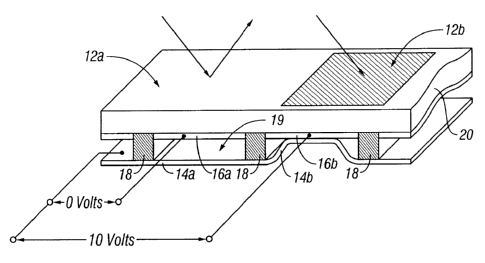
S Figure 1 is an isometric view depicting two adjacent pixels in a series of
pixels of a
visual display, wherein each pixel comprises a MEMS interferometric modulator.
In some
embodiments, an interferometric modulator display comprises a row/column array
of these
interferometric modulators. Each interferometric modulator includes a pair of
reflective layers
positioned at a variable and controllable distance from each other to form a
resonant optical
cavity with at least one variable dimension. In one embodiment, one of the
reflective layers may
be moved between two positions. In the first position, referred to herein as
the released state, the
movable layer is positioned at a relatively large distance from a fixed
partially reflective layer. In
the second position, the movable layer is positioned more closely adjacent to
the partially
reflective layer. Incident light that reflects from the two layers interferes
constructively or
destructively depending on the position of the movable reflective layer,
producing either an
overall reflective or non-reflective state for each pixel.
The depicted portion of the pixel array in Figure 1 includes two adjacent
interferometric
modulators 12a and 12b. In the interferometric modulator 12a on the left, a
movable and highly
reflective layer 14a is illustrated in a released position at a predetermined
distance from a fixed
partially reflective layer 16a. In the interferometric modulator 12b on the
right, the movable
highly reflective layer 14b is illustrated in an actuated position adjacent to
the fixed partially
reflective layer 16b.
The fixed layers 16a, 16b are electrically conductive, partially transparent
and partially
reflective, and may be fabricated, for example, by depositing one or more
layers each of
chromium and indium-tin-oxide onto a transparent substrate 20. The layers are
patterned into
parallel strips, and may form row electrodes in a display device as described
further below. The
movable layers 14a, 14b may be formed as a series of parallel strips of a
deposited metal layer or
layers (orthogonal to the row electrodes 16a, 16b) deposited on top of posts
18 and an intervening
sacrificial material deposited between the posts 18. When the sacrificial
material is etched away,
the deformable metal layers are separated from the fixed metal layers by a
defined air gap 19. A
highly conductive and reflective material such as aluminum may be used for the
deformable
layers, and these strips may form column electrodes in a display device.
With no applied voltage, the cavity 19 remains between the layers 14a, 16a and
the
deformable layer is in a mechanically relaxed state as illustrated by the
pixel 12a in Figure 1.
However, when a potential difference is applied to a selected row and column,
the capacitor
formed at the intersection of the row and column electrodes at the
corresponding pixel becomes
-4-
CA 02513026 2005-07-22
charged, and electrostatic forces pull the electrodes together. If the voltage
is high enough, the
movable layer is deformed and is forced against the fixed layer (a dielectric
material which is not
illustrated in this Figure may be deposited on the fixed layer to prevent
shorting and control the
separation distance) as illustrated by the pixel 12b on the right in Figure 1.
The behavior is the
same regardless of the polarity of the applied potential difference. In this
way, row/column
actuation that can control the reflective vs. non-reflective pixel states is
analogous in many ways
to that used in conventional LCD and other display technologies.
Figures 2 through 5 illustrate one exemplary process and system for using an
array of
interferometric modulators in a display application. Figure 2 is a system
block diagram
illustrating one embodiment of an electronic device that may incorporate
aspects of the invention.
In the exemplary embodiment, the electronic device includes a processor 21
which may be any
general purpose single- or multi-chip microprocessor such as an ARM, Pentium~,
Pentium H'~,
Pentium III°, Pentium IVY, Pentium Pro, an 8051, a MIPS~, a Power PC~,
an ALPHA~, or any
special purpose microprocessor such as a digital signal processor,
microcontroller, or a
1 S programmable gate array. As is conventional in the art, the processor 21
may be configured to
execute one or more software modules. In addition to executing an operating
system, the
processor may be configured to execute one or more software applications,
including a web
browser, a telephone application, an email program, or any other software
application.
In one embodiment, the processor 21 is also configured to communicate with an
array
controller 22. In one embodiment, the array controller 22 includes a row
driver circuit 24 and a
colunm driver circuit 26 that provide signals to a pixel array 30. The cross
section of the array
illustrated in Figure 1 is shown by the lines 1-1 in Figure 2. For MEMS
interferometric
modulators, the row/column actuation protocol may take advantage of a
hysteresis property of
these devices illustrated in Figure 3. It may require, for example, a 10 volt
potential difference to
cause a movable layer to deform from the released state to the actuated state.
However, when the
voltage is reduced from that value, the movable layer maintains its state as
the voltage drops back
below 10 volts. In the exemplary embodiment of Figure 3, the movable layer
does not release
completely until the voltage drops below 2 volts. There is thus a range of
voltage, about 3 to 7 V
in the example illustrated in Figure 3, where there exists a window of applied
voltage within
which the device is stable in either the released or actuated state. This is
referred to herein as the
"hysteresis window" or "stability window." For a display array having the
hysteresis
characteristics of Figure 3, the row/column actuation protocol can be designed
such that during
row strobing, pixels in the strobed row that are to be actuated are exposed to
a voltage difference
of about 10 volts, and pixels that are to be released are exposed to a voltage
difference of close to
zero volts. After the strobe, the pixels are exposed to a steady state voltage
difference of about 5
volts such that they remain in whatever state the row strobe put them in.
After being written,
-5-
CA 02513026 2005-07-22
each pixel sees a potential difference within the "stability window" of 3-7
volts in this example.
This feature makes the pixel design illustrated in Figure 1 stable under the
same applied voltage
conditions in either an actuated or released pre-existing state. Since each
pixel of the
interferometric modulator, whether in the actuated or released state, is
essentially a capacitor
S formed by the fixed and moving reflective layers, this stable state can be
held at a voltage within
the hysteresis window with almost no power dissipation. Essentially no current
flows into the
pixel if the applied potential is fixed.
In typical applications, a display frame may be created by asserting the set
of column
electrodes in accordance with the desired set of actuated pixels in the first
row. A row pulse is
then applied to the row 1 electrode, actuating the pixels corresponding to the
asserted column
lines. The asserted set of column electrodes is then changed to correspond to
the desired set of
actuated pixels in the second row. A pulse is then applied to the row 2
electrode, actuating the
appropriate pixels in row 2 in accordance with the asserted column electrodes.
The row 1 pixels
are unaffected by the row 2 pulse, and remain in the state they were set to
during the row 1 pulse.
This may be repeated for the entire series of rows in a sequential fashion to
produce the frame.
Generally, the frames are refreshed and/or updated with new display data by
continually
repeating this process at some desired number of frames per second. A wide
variety of protocols
for driving row and column electrodes of pixel arrays to produce display
frames are also well
known and may be used in conjunction with the present invention.
Figures 4 and 5 illustrate one possible actuation protocol for creating a
display frame on
the 3x3 array of Figure 2. Figure 4 illustrates a possible set of column and
row voltage levels that
may be used for pixels exhibiting the hysteresis curves of Figure 3. In the
Figure 4 embodiment,
actuating a pixel involves setting the appropriate column to -Vb;as, and the
appropriate row to
+4V, which may correspond to -5 volts and +5 volts respectively Releasing the
pixel is
accomplished by setting the appropriate column t0 +Vb;as, and the appropriate
row to the same
+0V, producing a zero volt potential difference across the pixel. In those
rows where the row
voltage is held at zero volts, the pixels are stable in whatever state they
were originally in,
regardless of whether the column is at +Vb;as, or -Vb;as~ As is also
illustrated in Figure 4, it will be
appreciated that voltages of opposite polarity than those described above can
be used, e.g.,
actuating a pixel can involve setting the appropriate column t0 +Vb;am and the
appropriate row to
-OV. In this embodiment, releasing the pixel is accomplished by setting the
appropriate column
to -Vb;as, and the appropriate row to the same -OV, producing a zero volt
potential difference
across the pixel.
Figure SB is a timing diagram showing a series of row and column signals
applied to the
3x3 array of Figure 2 which will result in the display arrangement illustrated
in Figure SA, where
actuated pixels are non-reflective. Prior to writing the frame illustrated in
Figure SA, the pixels
CA 02513026 2005-07-22
can be in any state, and in this example, all the rows are at 0 volts, and all
the columns are at +$
volts. With these applied voltages, all pixels are stable in their existing
actuated or released
states.
In the Figure SA frame, pixels (1,l), (1,2), (2,2), (3,2) and (3,3) are
actuated. To
$ accomplish this, during a "line time" for row 1, columns 1 and 2 are set to -
5 volts, and column 3
is set to +$ volts. This does not change the state of any pixels, because all
the pixels remain in
the 3-7 volt stability window. Row 1 is then strobed with a pulse that goes
from 0, up to 5 volts,
and back to zero. This actuates the (1,1) and (1,2) pixels and releases the
(1,3) pixel. No other
pixels in the array are affected. To set row 2 as desired, column 2 is set to -
5 volts, and columns
1 and 3 are set to +$ volts. The same strobe applied to row 2 will then
actuate pixel (2,2) and
release pixels (2,1) and (2,3). Again, no other pixels of the array are
affected. Row 3 is similarly
set by setting columns 2 and 3 to -5 volts, and column 1 to +$ volts. The row
3 strobe sets the
row 3 pixels as shown in Figure SA. After writing the frame, the row
potentials are zero, and the
column potentials can remain at either +$ or -5 volts, and the display is then
stable in the
arrangement of Figure $A. It will be appreciated that the same procedure can
be employed for
arrays of dozens or hundreds of rows and columns. It will also be appreciated
that the timing,
sequence, and levels of voltages used to perform row and column actuation can
be varied widely
within the general principles outlined above, and the above example is
exemplary only, and any
actuation voltage method can be used with the present invention.
The details of the structure of interferometric modulators that operate in
accordance with
the principles set forth above may vary widely. For example, Figures 6A-6C
illustrate three
different embodiments of the moving mirror structure. Figure 6A is a cross
section of the
embodiment of Figure l, where a strip of metal material 14 is deposited on
orthogonally
extending supports 18. In Figure 6B, the moveable reflective material 14 is
attached to supports
at the corners only, on tethers 32. In Figure 6C, the moveable reflective
material 14 is suspended
from a deformable layer 34. This embodiment has benefits because the
structural design and
materials used for the reflective material 14 can be optimized with respect to
the optical
properties, and the structural design and materials used for the deformable
layer 34 can be
optimized with respect to desired mechanical properties. The production of
various types of
interferometric devices is described in a variety of published documents,
including, for example,
U.S. Published Application 2004/0051929. A wide variety of well known
techniques may be
used to produce the above described structures involving a series of material
deposition,
patterning, and etching steps.
Electrical Characterization
In some embodiments, methods are provided for testing the electrical
characteristics of
an interferometric modulator display. In some cases, the resistance across
conductive leads in the
_7_
CA 02513026 2005-07-22
display is measured. Resistance measurements can indicate whether the
conductive leads were
properly formed during the manufacturing process and whether any debris within
the display is
altering the electrical characteristics. For example, it is desirable that the
resistance through each
individual conductive lead (e.g., each row and column conductive lead) be low.
A high
resistance through an individual conductive lead may be indicative of an open
within the lead. It
is also desirable that the resistance between adjacent conductive leads be
high. For example, a
low resistance between a column and a row conductive lead may indicate that a
short exists in the
interferometric modulator element that is formed at the intersection of the
column and row.
Similarly, a low resistance between adjacent column or row conductive leads
may be indicative
of a short between those leads. Shorts may be caused by an error in
manufacturing that causes
the conductive material to be fused together or by conductive debris between
the leads.
Measuring resistance in conductive leads in an interferometric modulator
display
includes determining the resistance in view of the fact that the electrical
characteristics of the
display can vary depending on whether the interferometric modulator elements
are actuated or
not. In typical resistance meters, such as those typically used to test liquid
crystal displays, the
voltage applied to make the measurement may vary. Accordingly, the voltage may
rise to levels
sufficient to actuate interferometric modulators within the display, which may
result in different
measurements from those obtained when the interferometric modulators do not
actuate. Thus, in
one embodiment, resistance is measured by applying a controlled voltage across
the leads and
then measuring the resulting current, known as a force voltage/measure current
(FVMI)
technique, when the interferometric modulators are in a non-actuated state. By
applying a
controlled voltage, actuation of the interferometric modulators can be
controlled. In one
embodiment, such resistance measurements may be made using a Keithly 6517 high
resistance
meter.
Figure 7 is a flowchart illustrating a method of measuring resistance between
conductive
leads in a display such as an interferometric modulator display. Depending on
the particular
embodiment, steps may be added to those depicted in Figure 7 or some steps may
be removed. In
addition, the order of steps may be rearranged depending on the application.
At step 200, a
controlled voltage is applied across at least two conductive leads of the
display. In one
embodiment, multiple leads are interfaced to external electronics and the
leads to which the
controlled voltage is applied is determined by the external electronics. For
example, all leads in
the display could be coupled to external electronics containing relays, which
could be used for
selectively applying a controlled voltage to less than all leads in the
display. In some
embodiments, the external electronics can be used to short one or more leads
together. In one
embodiment when an interferometric modulator is being tested, the applied
controlled voltage is
kept low enough such that no interferometric modulators actuate. For example,
the voltage may
_g_
CA 02513026 2005-07-22
be kept within +/- 1 V. Next, at step 202, the resulting current is measured
through the
conductive leads, after which resistance may be determined. In one embodiment,
resistance is
measured through one or more conductive leads, such as through a row or
column, by applying a
voltage to opposite ends of the rows or columns. Such a measurement allows
determination of
S whether an open exists in the rows or columns. In another embodiment,
resistance is measured
between a row and a column. Such a measurement allows determination of whether
a short exists
between the row and column in the interferometric modulator element at the
intersection of the
row or column. In one embodiment, a resistance of less than 100 MS2 indicates
that unacceptable
conduction exists between a row and column. In another embodiment, a
resistance of less than
50 MS2 indicates that unacceptable conduction exists between a row and column.
In another
embodiment, resistance is measured between adjacent rows and/or columns. Such
a
measurement allows determination of whether a short exists between the
adjacent rows or
columns. In one embodiment, a resistance of less than 10 MS2 indicates that
unacceptable
conduction exists between adjacent rows or columns. In another embodiment, a
resistance of less
than 1 MS2 indicates an unacceptable conduction between adjacent rows or
columns.
In some embodiments, resistance measurements may be made on multiple
conductive
leads simultaneously. For example, resistance may be measured between all
adjacent rows
simultaneously. If the per lead resistance measured in this way is less than a
predefined
threshold, then subsequent testing may optionally be used to identify which
row-row leads
contain a short. Similarly, the resistance of all adjacent column leads may be
measured
simultaneously or the row-to-column resistance through pixel elements may be
measured
simultaneously. In some embodiments, the display being tested is a color
display. In such cases,
the resistance between adjacent leads may include measuring resistance between
leads for driving
different color subpixels, such as between a lead for red subpixels and a lead
for green and/or
blue subpixels. Accordingly, in some embodiments, measuring resistance between
adjacent
column leads may involve three separate measurements-the red-blue leads, blue-
green leads,
and red-green leads.
In some embodiments, the controlled voltage is a time-varying voltage
waveform. For
example, in some embodiments, an AC waveform is applied. A time-varying
voltage waveform
that is symmetric about some constant value may be used to ensure that a net
zero charge is
supplied to display elements. For example, when applying the voltage to a row
and column to
measure for shorts through a display element at the row-column intersection, a
voltage waveform
symmetric about 0 V or an offset voltage (e.g., the voltage required for zero
charge in a display
element) may be applied to ensure no build up of charge in the display element
during testing.
In one embodiment, resistance is measured separately for each polarity. The
comparison
of resistances measured for opposite polarities may provide a check of quality
of the display. For
-9-
CA 02513026 2005-07-22
example, in an interferometric modulator display, the driving schemes may
involve applying
voltages of both polarities as described above. Accordingly, it may be
desirable for the electrical
characteristics of the display to be similar for both polarities. Furthermore,
measuring resistance
in both polarities may provide a check to determine whether detected values
are due to noise or
due to actual resistance. For example, if the resistance is very high, only
noise may be measured.
If the polarity of the measured current does not change sign upon reversal of
the polarity of the
applied voltage, there may be indication that only noise is being detected.
The resistance measurement may optionally be used to identify the display as
having the
electrical characteristics desirable for use as a display. Thus, for example,
proceeding to step 204
in Figure 7, the resistance measurements or number of shorts and/or opens are
compared to
predefined thresholds. If the measurements or numbers are within the
thresholds, then the
display may be used as a display by proceeding to step 206. If the
measurements or numbers are
not within the thresholds, then the display may be deemed defective and
discarded at step 208.
Such testing may be used for quality control purposes during manufacture of
the displays. In
some embodiments, a sampling of displays produced during manufacturing is
tested to represent
the quality of one or more lots of displays.
In other embodiments, resistance measurements may be used to identify errors
in
manufacturing. For example, resistance measurements may be used to pinpoint
locations of
manufacturing error. If a pinpointed location of error, such as a short
through a single pixel, is
repeatedly measured at the same location in different displays, there may be
an indication of a
manufacturing error. This information may be used to correct defects in
equipment or procedure.
In some embodiments, resistance measurements may be used to monitor the
results of
certain manufacturing processes. For example, resistance measurements may be
used to monitor
variation in film parameters (e.g., thickness and width dimensions).
In some embodiments, the precise location of a short or open may be determined
through
a decision tree approach. For example, all leads may be measured at a first
level of the decision
tree. If the measured resistance indicates that a short exists somewhere in
the display, half of the
row or column leads may then be tested followed by the other half if the short
or open was not
detected in the first half. In this way, the location of the fault is narrowed
down to half of the
display. This process may continue in a similar fashion to narrow down the
location of the fault
until it is precisely identified through a single row and/or column. In other
embodiments, each
row and/or column combination may be separately measured to determine the
location of faults.
In still other embodiments, bypass structures may be incorporated within a
display that
enables one or more pixels to be bypassed. Thus, for example, if a resistance
measurement
indicates a short at one pixel site, that pixel may be bypassed by activating
a bypass structure that
shunts the conductive row and column leads at the pixel around the pixel site,
thus electrically
-10-
CA 02513026 2005-07-22
isolating the bad pixel. Accordingly, in one embodiment, resistance
measurement procedures
such as described herein are used to provide an indication of which pixels or
regions of a display
to bypass with an appropriate bypass structure.
Electrical Measurement Structures
In some embodiments, appropriate conductive structures are interfaced to an
interferometric modulator array during manufacturing in order to facilitate
electrical and electro-
optical characterization and testing of the array. In one embodiment, depicted
in Figure 8, row
and column leads 400 may be connected to one or more buss bars 410, which are
then connected
to one or more test pads 420. Row and column leads 400 may correspond, for
example, to the
row and column strips depicted in Figure SA. The buss bars 410 electrically
connect all the leads
connected to the bar and thus facilitate the voltage control of all those
leads simultaneously. It
may also be desirable that all leads are shorted together during processing by
using a shorting bar
430. The shorting bar 430 may be removed prior to electrical and/or electro-
optical testing. In
one embodiment, alternating row and column leads 400 are connected to the same
buss bars 410
(i.e., interdigitated), as depicted in Figure 8, to allow for measurement of
adjacent row-row or
column-column resistances as described above. As used herein, a "row" refers
to the conducting
lines adjacent to the substrate (e.g., lines of transparent conductor). As
used herein, a "column"
refers to the conducting lines associated with the movable mirrors. In other
embodiments,
alternative arrangements of shorting bars and test pads may be used. For
example, the
arrangement in Figure 9 provides test pads 510 on opposite ends of the same
row and column
(e.g., test pads L1-L2, L3-L4, L7-L8, and LS-L6). Arrangements of buss bars
520 and test pads
530 may also be used to test different regions of the display separately. When
an interferometric
modulator display is a color display, buss bars and test pads may be
constructed so that the
different color subpixels (i.e., interferometric modulators designed to
reflect a certain color) can
be driven separately. After testing, the buss bars and test pads may be
removed so that the active
area (interferometric modulator array) can be incorporated into the desired
user package. In an
alternative embodiment, probes are contacted to each lead separately rather
than through test
pads. In this embodiment, external electronics may be used to short multiple
leads together in
order to simultaneously measure resistance through multiple leads. Those of
skill in the art will
recognize many suitable structures and techniques that can be used to
interface an interferometric
modulator array to a resistance measuring device.
In one embodiment, structures such as described in Figure 8 and 9 are used to
measure
resistance across single row and/or column lines (e.g., across L1-L2, L3-L4,
L7-L8, and L5-L6)
individually. A resistance that is too large may indicate a break in the row
or column line and
thus that at least a portion of the row or column cannot be matrix addressed.
In one embodiment,
structures such as described in Figure 8 and 9 are used to measure row-to-row
and/or column-to-
-11-
CA 02513026 2005-07-22
column resistance. If the rows and/or columns are interdigitated, then
resistance measurement
between adjacent rows and/or columns will provide a measurement of current
leakage (e.g.,
measured across R1-R2 or Cl-C2 in Figure 8). In some embodiments, if total row-
row or
column-column resistance is too low, individual sets of adjacent row-row or
column-column
resistance may be measured. In one embodiment, row-to-column resistance is
measured. This
measurement may be made by measuring resistance between all rows shorted and
all columns
shorted (e.g., between R1 and R2 shorted and C1 and C2 shorted in Figure 8).
Resistance that is
too low may indicate a short between a row and a column.
Interferometric Modulator Conditioning
In one embodiment, performance of an interferometric modulator display after
manufacture may be improved by preconditioning the display. The
preconditioning may be
accomplished by applying a voltage to the display sufficient to actuate
interferometric modulator
elements in the display. Immediately after manufacture, the voltages at which
interferometric
modulators actuate may vary until a steady state behavior is reached. Thus,
preconditioning may
stress the movable interferometric modulator elements so that a stable or near
stable response is
achieved upon actuation. Furthermore, such preconditioning may remove
transitory shorts
between conductive leads by vaporizing conductive debris. In some embodiments,
preconditioning may reveal defects not observed prior to preconditioning.
Thus, for example,
resistance measurements such as described above may be conducted both before
and after
preconditioning.
In one embodiment, the preconditioning voltage waveform is applied to
substantially all
elements in the interferometric modulator display simultaneously. In such a
manner, each
element may be stressed and conditioned identically so that the display
response of each element
is similar, reducing the observance of ghosting effects.
In one embodiment, a voltage waveform is applied to the display having an
amplitude
sufficient to actuate the interferometric modulators. The voltage may be
applied to all
interferometric modulators simultaneously (e.g., by applying the voltage
between Rl and R2
shorted to ground and C1 and C2 shorted to a waveform generator in Figure 8)
or to a subset of
the interferometric modulators. In one embodiment, a voltage waveform that is
symmetric about
some constant value may be used to ensure that a net zero charge is supplied
to the display
elements. For example, a voltage waveform symmetric about 0 V or an offset
voltage (e.g., the
voltage required for zero charge in a display element) may be applied to
ensure no build up of
charge in the display elements.
In one embodiment, the voltage waveform includes pulsing of an alternating
square
waveform. Figure IOA illustrates one such possible voltage waveform. A series
of square waves
having amplitudes 600 sufficient to actuate the interferometric modulators may
be applied. Thus,
-12-
CA 02513026 2005-07-22
when the voltage is at the positive 600 or negative 602 amplitude values, the
interferometric
modulators are actuated. When the voltage is at the offset potential 604, the
interferometric
modulators are in a non-actuated state. Each square waveform may have width
606 (e.g., 5 ms)
before the polarity of the applied voltage is reversed. A series of such
alternating square
waveforms may have width 608 (e.g., 0.5 s). After applying this sequence, the
voltage may be
held at the offset potential 604 for time 610 (e.g., 0.5 s). Thus, the result
of the waveform in
Figure 10A is that interferometric modulators will cycle through the sequence
of an actuated state
for time 608 followed by a non-actuated state for time 610. By making the
waveform symmetric
about the offset voltage 604 and quickly varying the amplitude between
positive and negative
polarities when driving the interferometric modulators in an actuated state,
no net charge is
accumulated in the interferometric modulators. Those of skill in the art will
recognize many
variations of this waveform. For example, time periods 606, 608, and 610 may
be varied to
obtain different frequency of actuation pulsing (e.g., by varying times 608
and/or 610) and
polarity pulsing (e.g., by varying time 606). In various embodiments, the
actuation frequency
may be at least about 0.1 Hz., 0.5 Hz, 1 Hz, 10 Hz, 50 Hz, 100 Hz, 500 Hz, or
1 kHz. In various
embodiments, the polarity change frequency may be at least about 100 Hz, 1
kHz, 5 kHz, 10 kHz,
50 kHz, 100 kHz, 500 kHz, and 1 MHz. Furthermore, in some embodiments, a
single actuation
waveform having alternating polarity is applied (e.g., only period 608). .
In another embodiment, the voltage waveform includes a triangular waveform.
Figure
lOB illustrates one such possible waveform. The amplitudes 650 of the
triangular waveform are
high enough such that the interferometric modulators actuate before the
amplitudes are reached.
In one embodiment, amplitudes that are about 10% higher than the required
actuation voltage are
used. The interferometric modulators will de-actuate before the voltage
reaches the offset
voltage 652 about which the interferometric modulators are centered. In
various embodiments,
the frequency of the triangle waveform may be at least about 0.1 Hz., 0.5 Hz,
1 Hz, 10 Hz, SO Hz,
100 Hz, 500 Hz, or 1 kHz.
Those of skill in the art will recognize many possible actuation voltage
waveforms that
may be used to precondition interferometric modulators. Thus, the disclosure
is not limited to
only square and triangular waveforms having the characteristics described
above.
In some embodiments, different waveforms are combined in series to create a
more
complex waveform string. For example, the triangle and square waveforms
described above may
be combined in series. In one embodiment, the triangle waveform is applied for
a first time
period (e.g., about 1 minute) followed by multiple sequences of square
waveforms (e.g., each
about 1 minute with increasing amplitudes) followed by a second triangle
waveform. This
sequence may be repeated any number of times or varied to produce any number
of waveform
combinations. Those of skill in the art will recognize many other voltage
waveforms and
-13-
CA 02513026 2005-07-22
combinations of waveforms that may be applied to result in conditioning of the
interferometric
modulator elements in a display.
In various embodiments, variations in preconditioning voltage waveforms
include
varying the length of time a particular waveform is applied, varying the
frequency of the
S waveform, and varying the amplitude of the waveform.
In some embodiments, if electrical characterization such as described above
indicates that
an interferometric modulator display is unsatisfactory, conditioning may be
employed to improve
the characteristics. For example, conditioning may remove shorts measured
during electrical
characterization. Thus, in one embodiment, electrical characterization is
conducted both before
and after conditioning to determine if any faulty characteristics have been
corrected by
conditioning.
Although the invention has been described with reference to embodiments and
examples,
it should be understood that numerous and various modifications can be made
without departing
from the spirit of the invention. Accordingly, the invention is limited only
by the following
claims.
-14-