Note: Descriptions are shown in the official language in which they were submitted.
CA 02513030 2005-07-22
Interncl Reference: IRDM.020 NON-EP / IDC-0035
METHOD AND SYSTEM FOR PACKAGING A MEMS DEVICE
Field
The field of the invention relates to microelectromechanical systems (MEMS).
Embodiments of the invention relate to micro-electro-mechanical systems (MEMS)
and methods
for packaging such systems. More specifically, the invention relates to
packaging an
interferometric modulator using a backplate that also holds electronic
circuitry connected to the
modulator.
Background
Consumers generally desire that electronic products be as small and
lightweight as
possible. As flat panel displays grow in capability and widespread
application, it is not unusual
for the size of a product to be driven by the size of the display, with great
pressure to make the
rest of the product fit within a minimal volume. Two dimensions of that volume
are frequently
defined by the 2D footprint of the flat panel display. With the increasing
desirability of product
"thinness," it becomes increasingly desirable to make thinner layers, to
combine layers, and/or to
eliminate layers from the product. Examples of product layers include, but are
not limited to,
clear windows to protect the display, airgaps between the protective window
and the display,
frontlights in front of the display, touch screens, plastic films with optical
functionalities, the
display front glass, the active layers of the display, the display back glass,
backlights behind the
display, PC boards, plastic films carrying interconnections, and plastic and
metal layers
comprising the physical enclosure of the product.
The predominant display used in manufacturing handheld portable electronic
devices is
currently the Liquid Crystal Display (LCD). The principal layers of the LCD
include a front
glass, a back glass, and several plastic optical films. Due to the nature of
an LCD, both the front
plate and the back plate of the LCD serve as active or functional components
of the LCD, placing
limitations on the degree to which layers can be combined, eliminated, and/or
replaced with a
thinner layer in order to decrease the thickness of the overall display. In
addition, the active
nature of both plates of an LCD places limitations on the materials which can
be used in those
plates, and therefore the strength and durability of the plates. If additional
strength and/or
protection is required beyond what can be provided using materials suitable
for the LCD plates,
other layers of material may be required in addition to the LCD plates,
potentially adding to the
thickness, weight, and cost of the device.
CA 02513030 2005-07-22
Microelectromechanical systems (MEMS) include micro mechanical elements,
actuators,
and electronics. Micromechanical elements may be created using deposition,
etching, and or
other micromachining processes that etch away parts of substrates and/or
deposited material
layers or that add layers to form electrical and electromechanical devices.
One type of MEMS
device is called an interferometric modulator. An interferometric modulator
may comprise a pair
of conductive plates, one or both of which may be transparent and/or
reflective in whole or part
and capable of relative motion upon application of an appropriate electrical
signal. One plate
may comprise a stationary layer deposited on a substrate, the other plate may
comprise a metallic
membrane separated from the stationary layer by an air gap. Such devices have
a wide range of
applications, and it would be beneficial in the art to utilize and/or modify
the characteristics of
these types of devices so that their features can be exploited in improving
existing products and
creating new products that have not yet been developed.
Summary
The system, method, and devices of the invention each have several aspects, no
single
one of which is solely responsible for its desirable attributes. Without
limiting the scope of this
invention, its more prominent features will now be discussed briefly. After
considering this
discussion, and particularly after reading the section entitled "Detailed
Description of Certain
Embodiments" one will understand how the features of this invention provide
advantages over
other display devices.
In one embodiment, for example, a display is provided, including a transparent
substrate,
an array of interferometric modulators configured to reflect light through
said transparent
substrate, a backplate sealed to the transparent substrate and providing a
cavity for said
interferometric modulators, and electronic circuitry located on the backplate
and in electrical
connection with the array of interferometric modulators.
In another embodiment, a device having a display is provided, including a
transparent
substrate, an array of interferometric modulators configured to reflect light
through the
transparent substrate, and a backplate sealed to the transparent substrate and
providing a cavity
for the interferometric modulators, wherein the backplate comprises electronic
circuitry
configured to control the interferometric modulators. In further embodiments,
the backplane
serves as a primary structural component of the display, and provides physical
support for
additional electronic circuitry configured to control the display.
In another embodiment, a method of manufacturing a display device is provided,
including providing a transparent substrate comprising an array of
interferometric modulators,
providing a backplate comprising electronic circuitry configured to control
the array of
interferometric modulators, sealing the transparent substrate to the backplate
so that a cavity is
-2-
CA 02513030 2005-07-22
formed above the array of interferometric modulators, and wherein the
electronic circuitry is
placed in electrical communication with the array of interferometric
modulators. In another
embodiment, a device is provided, the device being produced by the above
method.
In another embodiment, a display is provided, including means for modulating
light and
reflecting it towards a viewer, a first means for supporting the modulating
means, means for
controlling the state of the modulation means, a second means for supporting
the controlling
means and providing a cavity for the modulating means.
In another embodiment, a display for an electronic device is provided,
including a first
transparent substrate, a first array of interferometric modulators configured
to reflect light
through the first transparent substrate and in a first direction, a backplate
sealed to the first
transparent substrate and providing a cavity for the first array of
interferometric modulators,
wherein the backplate comprises electronic circuitry configured to control the
first array of
interferometric modulators, and a second transparent substrate sealed to the
backplate, wherein
the second transparent substrate comprises a second array of interferometric
modulators
configured to reflect light in a second direction, and wherein the first
direction and the second
direction are opposite directions.
In another embodiment, a display for an electronic device is provided,
including a first
transparent substrate, a first array of interferometric modulators configured
to reflect light
through the first transparent substrate and in a first direction, a backplate
sealed to the first
transparent substrate and providing a cavity for the first array of
interferometric modulators,
wherein the backplate comprises electronic circuitry configured to control the
first array of
interferometric modulators, and a second transparent substrate sealed to the
first backplane,
wherein the second transparent substrate comprises a second array of
interferometric modulators
configured to reflect light in a second direction, and wherein the first
direction and the second
direction are opposite directions.
In another embodiment, a device having a display is provided, including a
first
transparent substrate, a first array of interferometric modulators configured
to reflect light
through said first transparent substrate, a second transparent substrate
opposed to the first
transparent substrate, and a second array of interferometric modulators
configured to reflect light
through the second transparent substrate.
In another embodiment, a method of manufacturing a display is provided,
including
providing a first transparent substrate comprising a first array of
interferometric modulators,
providing a second transparent substrate comprising a first array of
interferometric modulators,
providing a backplate comprising electronic circuitry configured to control
the state of the first
and second arrays of interferometric modulators, sealing the first transparent
substrate to the
backplate, sealing the second transparent substrate to the backplate, and
placing the electronic
-3-
CA 02513030 2005-07-22
circuitry in electrical connection with the first and second arrays of
interferometric modulators.
In another embodiment, a display is provided, the device being manufactured by
the above
method.
In another embodiment, a display is provided, the display including a first
means for
modulating light and reflecting it towards a viewer; a first means for
supporting the first
modulating means; a second means for modulating light and reflecting it
towards a viewer; a
second means for supporting the second modulating means, means for controlling
the state of
said first and second modulation means, and a third means for supporting said
controlling means.
Brief Description of the Drawing-s
Figure 1 is an isometric view depicting a portion of one embodiment of an
interferometric modulator display in which a movable reflective layer of a
first interferometric
modulator is in a released position and a movable reflective layer of a second
interferometric
modulator is in an actuated position.
Figure 2 is a system block diagram illustrating one embodiment of an
electronic device
incorporating a 3x3 interferometric modulator display.
Figure 3 is a diagram of movable mirror position versus applied voltage for
one
exemplary embodiment of an interferometric modulator of Figure 1.
Figure 4 is an illustration of a set of row and column voltages that may be
used to drive
an interferometric modulator display.
Figures SA and SB illustrate one exemplary timing diagram for row and column
signals
that may be used to write a frame of display data to the 3x3 interferometric
modulator display of
Figure 3.
Figure 6A is a cross section of the device of Figure 1.
Figure 6B is a cross section of an alternative embodiment of an
interferometric
modulator.
Figure 6C is a cross section of another alternative embodiment of an
interferometric
modulator.
Figure 7 is an exploded view of an embodiment of a display in which a printed
circuit
carrier is bonded to a backplate.
Figure 8A is an assembled view of an embodiment of a display in which an
interferometric modulator carrier serves as the backplate and is connected to
an array of
interferometric modulators on a substrate.
Figure 8B is an assembled view of the embodiment of Figure 8A.
-4-
CA 02513030 2005-07-22
Figure 9A is a top view of the lower component of an embodiment of a display
in which
an interferometric modulator carrier serves as the backplate and is connected
to an array of
interferometric modulators on a substrate.
Figure 9B is a top view of the upper component of an embodiment of a display
in which
an interferometric modulator carrier serves as the backplate and is connected
to an array of
interferometric modulators on a substrate.
Figure 10A is an assembled view of an embodiment of a display in which an
interferometric modulator carrier serves as the backplate and is internally
connected to an array
of interferometric modulators on a substrate.
Figure lOB is an exploded view of the embodiment of Figure 10A.
Figure 11 is an exploded view of an embodiment of a display in which an
interferometric
modulator carrier serves as a backplate, and electronic components are located
on the same
surface of the substrate as the array of interferometric modulators.
Figure 12 is a cross-sectional view of one embodiment of a dual-screen display
in which
an interferometric modulator carrier is disposed between two substrates.
Figure 13 is a cross-sectional view of a dual-screen display in which a
substrate can
perform some of the same functions as an interferometric modulator carrier.
Figure 14 is a cross-sectional view of a dual-screen display having an annular
interferometric modulator carrier.
Figure 15 is a cross-sectional view of a dual-screen display without an
interferometric
modulator carrier.
Figure 16 is a cross-sectional view of a device in which the interferometric
modulator
carrier of a display can serve as the primary structural support for the
device.
Figure 17A is a perspective view of an embodiment of a display in which a
contoured
interferometric modulator carrier serves as a backplate.
Figure 17B is a cross-sectional view of the embodiment of Figure 17A.
Figures 18A and 18B are system block diagrams illustrating an embodiment of a
visual
display device comprising a plurality of interferometric modulators.
Detailed Description of Preferred Embodiments
One embodiment of the invention is an interferometric modulator-based display,
as
discussed in greater detail below, wherein the backplate includes active
components. Typically
in an interferometric modulator, the backplate serves a purely mechanical
function. Thus, fewer
constraints are placed on the materials which can be used in the backplate,
and there is greater
freedom for layers to be combined, eliminated, and/or replaced with alternate
or thinner layers.
In particular, in this embodiment the backplate may be employed to hold
electronic circuitry
-5-
CA 02513030 2005-07-22
which controls the state of the interferometric modulator. For example,
integrated circuits, such
as display driver chips, may be mounted directly onto the backplate and then
electrically
connected to the interferometric modulator. The backplate can also be used to
provide structural
support for a device enclosing the display. The use of a backplate for
multiple purposes
S advantageously permits the construction of an interferometric modulator-
based display which
may be thinner, stronger, easier to fabricate and/or less expensive than
displays based on other
technologies.
Another embodiment of the invention is an interferometric modulator-based
display that
has two opposed screens. The backplate of one display is used to form an
interferometric
modulator that faces in the opposite direction. This can be used, for example,
in a cellular
telephone that includes displays on opposite sides of the telephone. The use
of the backplate to
perform these functions advantageously permits the creation of dual-screen
displays which are
thinner, more rugged, and/or have a smaller footprint than other dual-screen
displays.
The following detailed description is directed to certain specific embodiments
of the
invention. However, the invention can be embodied in a multitude of different
ways. In this
description, reference is made to the drawings wherein like parts are
designated with like
numerals throughout. As will be apparent from the following description, the
invention may be
implemented in any device that is configured to display an image, whether in
motion (e.g., video)
or stationary (e.g., still image), and whether textual or pictorial. More
particularly, it is
contemplated that the invention may be implemented in or associated with a
variety of electronic
devices such as, but not limited to, mobile telephones, wireless devices,
personal data assistants
(PDAs), hand-held or portable computers, GPS receivers/navigators, cameras,
MP3 players,
camcorders, game consoles, wrist watches, clocks, calculators, television
monitors, flat panel
displays, computer monitors, auto displays (e.g., odometer display, etc.),
cockpit controls and/or
displays, display of camera views (e.g., display of a rear view camera in a
vehicle), electronic
photographs, electronic billboards or signs, projectors, architectural
structures, packaging, and
aesthetic structures (e.g., display of images on a piece of jewelry). MEMS
devices of similar
structure to those described herein can also be used in non-display
applications such as in
electronic switching devices.
One interferometric modulator display embodiment comprising an interferometric
MEMS display element is illustrated in Figure 1. In these devices, the pixels
are in either a
bright or dark state. In the bright ("on" or "open") state, the display
element reflects a large
portion of incident visible light to a user. When in the dark ("off' or
"closed") state, the display
element reflects little incident visible light to the user. Depending on the
embodiment, the light
reflectance properties of the "on" and "off' states may be reversed. MEMS
pixels can be
-6-
CA 02513030 2005-07-22
configured to reflect predominantly at selected colors, allowing for a color
display in addition to
black and white.
Figure 1 is an isometric view depicting two adjacent pixels in a series of
pixels of a
visual display, wherein each pixel comprises a MEMS interferometric modulator.
In some
embodiments, an interferometric modulator display comprises a row/column array
of these
interferometric modulators. Each interferometric modulator includes a pair of
reflective layers
positioned at a variable and controllable distance from each other to form a
resonant optical
cavity with at least one variable dimension. In one embodiment, one of the
reflective layers may
be moved between two positions. In the first position, referred to herein as
the released state, the
movable layer is positioned at a relatively large distance from a fixed
partially reflective layer. In
the second position, the movable layer is positioned more closely adjacent to
the partially
reflective layer. Incident light that reflects from the two layers interferes
constructively or
destructively depending on the position of the movable reflective layer,
producing either an
overall reflective or non-reflective state for each pixel.
The depicted portion of the pixel array in Figure 1 includes two adjacent
interferometric
modulators 12a and 12b. In the interferometric modulator 12a on the left, a
movable and highly
reflective layer 14a is illustrated in a released position at a predetermined
distance from a fixed
partially reflective layer 16a. In the interferometric modulator 12b on the
right, the movable
highly reflective layer 14b is illustrated in an actuated position adjacent to
the fixed partially
reflective layer 16b.
The fixed layers 16a, 16b are electrically conductive, partially transparent
and partially
reflective, and may be fabricated, for example, by depositing one or more
layers each of
chromium and indium-tin-oxide onto a transparent substrate 20. The layers are
patterned into
parallel strips, and may form row electrodes in a display device as described
further below. The
movable layers 14a, 14b may be formed as a series of parallel strips of a
deposited metal layer or
layers orthogonal to the row electrodes 16a, 16b) deposited on top of posts 1
g and an
intervening sacrificial material deposited between the posts 18. When the
sacrificial material is
etched away, the deformable metal layers are separated from the fixed metal
layers by a defined
air gap 19. A highly conductive and reflective material such as aluminum may
be used for the
deformable layers, and these strips may form column electrodes in a display
device.
With no applied voltage, the cavity 19 remains between the layers 14a, 16a and
the
deformable layer is in a mechanically relaxed state as illustrated by the
pixel 12a in Figure 1.
However, when a potential difference is applied to a selected row and column,
the capacitor
formed at the intersection of the row and column electrodes at the
corresponding pixel becomes
charged, and electrostatic forces pull the electrodes together. If the voltage
is high enough, the
movable layer is deformed and is forced against the fixed layer (a dielectric
material which is not
CA 02513030 2005-07-22
illustrated in this Figure may be deposited on the fixed layer to prevent
shorting and control the
separation distance) as illustrated by the pixel 12b on the right in Figure 1.
The behavior is the
same regardless of the polarity of the applied potential difference. In this
way, row/column
actuation that can control the reflective vs. non-reflective pixel states is
analogous in many ways
to that used in conventional LCD and other display technologies.
Figures 2 through 5 illustrate one exemplary process and system for using an
array of
interferometric modulators in a display application. Figure 2 is a system
block diagram
illustrating one embodiment of an electronic device that may incorporate
aspects of the invention.
In the exemplary embodiment, the electronic device includes a processor 21
which may be any
general purpose single- or mufti-chip microprocessor such as an ARM, Pentium ,
Pentium 1I~,
Pentium III~, Pentium IV~, Pentium Pro, an 8051, a MIPS~, a Power PC~, an
ALPHA~, or any
special purpose microprocessor such as a digital signal processor,
microcontroller, or a
programmable gate array. As is conventional in the art, the processor 21 may
be configured to
execute one or more software modules. In addition to executing an operating
system, the
processor may be configured to execute one or more software applications,
including a web
browser, a telephone application, an email program, or any other software
application.
In one embodiment, the processor 21 is also configured to communicate with an
array
controller 22. In one embodiment, the array controller 22 includes a row
driver circuit 24 and a
column driver circuit 26 that provide signals to a pixel array 30. The cross
section of the array
illustrated in Figure 1 is shown by the lines 1-1 in Figure 2. For MEMS
interferometric
modulators, the row/column actuation protocol may take advantage of a
hysteresis property of
these devices illustrated in Figure 3. It may require, for example, a 10 volt
potential difference to
cause a movable layer to deform from the released state to the actuated state.
However, when the
voltage is reduced from that value, the movable layer maintains its state as
the voltage drops back
below 10 volts. In the exemplary embodiment of Figure 3, the movable layer
does not release
completely until the voltage drops below 2 volts. There is thus a range of
voltage, about 3 to 7 V
in the example illustrated in Figure 3, where there exists a window of applied
voltage within
which the device is stable in either the released or actuated state. This is
referred to herein as the
"hysteresis window" or "stability window." For a display array having the
hysteresis
characteristics of Figure 3, the row/column actuation protocol can be designed
such that during
row strobing, pixels in the strobed row that are to be actuated are exposed to
a voltage difference
of about 10 volts, and pixels that are to be released are exposed to a voltage
difference of close to
zero volts. After the strobe, the pixels are exposed to a steady state voltage
difference of about 5
volts such that they remain in whatever state the row strobe put them in.
After being written,
each pixel sees a potential difference within the "stability window" of 3-7
volts in this example.
This feature makes the pixel design illustrated in Figure 1 stable under the
same applied voltage
-g-
CA 02513030 2005-07-22
conditions in either an actuated or released pre-existing state. Since each
pixel of the
interferometric modulator, whether in the actuated or released state, is
essentially a capacitor
formed by the fixed and moving reflective layers, this stable state can be
held at a voltage within
the hysteresis window with almost no power dissipation. Essentially no current
flows into the
pixel if the applied potential is fixed.
In typical applications, a display frame may be created by asserting the set
of column
electrodes in accordance with the desired set of actuated pixels in the first
row. A row pulse is
then applied to the row 1 electrode, actuating the pixels corresponding to the
asserted column
lines. The asserted set of column electrodes is then changed to correspond to
the desired set of
actuated pixels in the second row. A pulse is then applied to the row 2
electrode, actuating the
appropriate pixels in row 2 in accordance with the asserted column electrodes.
The row 1 pixels
are unaffected by the row 2 pulse, and remain in the state they were set to
during the row 1 pulse.
This may be repeated for the entire series of rows in a sequential fashion to
produce the frame.
Generally, the frames are refreshed and/or updated with new display data by
continually
repeating this process at some desired number of frames per second. A wide
variety of protocols
for driving row and column electrodes of pixel arrays to produce display
frames are also well
lrnown and may be used in conjunction with the present invention.
Figures 4 and 5 illustrate one possible actuation protocol for creating a
display frame on
the 3x3 array of Figure 2. Figure 4 illustrates a possible set of column and
row voltage levels that
may be used for pixels exhibiting the hysteresis curves of Figure 3. In the
Figure 4 embodiment,
actuating a pixel involves setting the appropriate column to -Vb;as, and the
appropriate row to
+0V, which may correspond to -S volts and +S volts respectively Releasing the
pixel is
accomplished by setting the appropriate column t0 +Vb;as, and the appropriate
row to the same
+0V, producing a zero volt potential difference across the pixel. In those
rows where the row
voltage is held at zero volts, the pixels are stable in whatever state they
were originally in,
regardless of whether the column is at +Vh;as, or -VS;a~.
Figure SB is a timing diagram showing a series of row and column signals
applied to the
3x3 array of Figure 2 which will result in the display arrangement illustrated
in Figure SA, where
actuated pixels are non-reflective. Prior to writing the frame illustrated in
Figure SA, the pixels
can be in any state, and in this example, all the rows are at 0 volts, and all
the columns are at +5
volts. With these applied voltages, all pixels are stable in their existing
actuated or released
states.
In the Figure SA frame, pixels (1,1), (1,2), (2,2), (3,2) and (3,3) are
actuated. To
accomplish this, during a "line time" for row 1, columns 1 and 2 are set to -S
volts, and column 3
is set to +S volts. This does not change the state of any pixels, because all
the pixels remain in
the 3-7 volt stability window. Row 1 is then strobed with a pulse that goes
from 0, up to 5 volts,
-9-
CA 02513030 2005-07-22
and back to zero. This actuates the (1,1) and (1,2) pixels and releases the
(1,3) pixel. No other
pixels in the array are affected. To set row 2 as desired, column 2 is set to -
5 volts, and columns
1 and 3 are set to +5 volts. The same strobe applied to row 2 will then
actuate pixel (2,2) and
release pixels (2,1) and (2,3). Again, no other pixels of the array are
affected. Row 3 is similarly
set by setting columns 2 and 3 to -5 volts, and column 1 to +5 volts. The row
3 strobe sets the
row 3 pixels as shown in Figure SA. After writing the frame, the row
potentials are zero, and the
column potentials can remain at either +5 or -S volts, and the display is then
stable in the
arrangement of Figure SA. It will be appreciated that the same procedure can
be employed for
arrays of dozens or hundreds of rows and columns. It will also be appreciated
that the timing,
sequence, and levels of voltages used to perform row and column actuation can
be varied widely
within the general principles outlined above, and the above example is
exemplary only, and any
actuation voltage method can be used with the present invention.
The details of the structure of interferometric modulators that operate in
accordance with
the principles set forth above may vary widely. For example, Figures 6A-6C
illustrate three
different embodiments of the moving mirror structure. Figure 6A is a cross
section of the
embodiment of Figure 1, where a strip of metal material 14 is deposited on
orthogonally
extending supports 18. In Figure 6B, the moveable reflective material 14 is
attached to supports
at the corners only, on tethers 32. In Figure 6C, the moveable reflective
material 14 is suspended
from a deforrnable layer 34. This embodiment has benefits because the
structural design and
materials used for the reflective material 14 can be optimized with respect to
the optical
properties, and the structural design and materials used for the deformable
layer 34 can be
optimized with respect to desired mechanical properties. The production of
various types of
interferometric devices is described in a variety of published documents,
including, for example,
U.S. Published Application 2004/0051929. A wide variety of well known
techniques may be
used to produce the above described structures involving a series of material
deposition,
patterning, and etching steps.
The lifetime of an interferometric modulator of the type discussed above can
be greatly
extended by protecting the interferometric modulator from mechanical
interference, excessive
moisture, and other potentially damaging substances. Embodiments of
interferometric
modulator-based displays utilize a backplate (also referred to as a backplane)
to provide this
protection. For example, the edge of a backplate can be attached with adhesive
near the edge of
the transparent substrate to prevent mechanical interference from reaching and
potentially
damaging the interferometric modulator elements fabricated on the backside of
the display glass.
Additionally, the backplate together with its adhesive attachment to the
transparent substrate
prevents moisture and other potentially detrimental gases, liquids and solids
from reaching the
interferometric modulator elements. Accordingly, the backplate can be
transparent or opaque,
-10-
CA 02513030 2005-07-22
conductive or insulating, essentially two-dimensional or projecting
appreciably into a third
dimension. In one embodiment, the backplate can be made of material completely
unsuitable for
use as a transparent display substrate, such as an opaque metal.
It can be seen in embodiments of interferometric-based displays, the backplate
need not
serve any role as an active or functional component of the display. Thus, a
minimal set of
requirements and specifications related to the functionality of the display
are placed on the
backplate. Consequently, there is significant freedom available in the
backplate design to address
other system needs and functions. Configurations in which the backplate is
employed for
multiple, non-packaging-related purposes are well suited for use in display-
centric products
which incorporate MEMS-based displays and associated ancillary components.
The backplate itself can be part of the display's lighting system. Any number
of RF-
related functions including but not limited to shielding, passive components,
and antennas can be
integrated into the backplate. As described herein, the backplate can be a PC
board, an
electronics layer, an electrical connection component, a battery, or merely a
mechanical
component to support or hold other components that serve various purposes in a
device. The
backplate can be used to implement any suitable function of the electronic
product. The
capabilities described above are possible since the nature of the
interferometric modulator display
imposes only a limited set of requirements on the backplate.
The backplate can be employed to hold electronics, and the footprint of the
back plate
can be expanded well beyond the active display area formed by the
interferometric modulator so
that the backplate essentially becomes a "backbone" for and the principal
structural element of
the device which contains the display. In some embodiments this is desirable
because the display
can be made much stronger than conventional displays that require glass
materials for a
backplate.
Accordingly, it is desirable to employ the backplate to perform various device
functions
or to impart desirable attributes to the devices. For example, the backplate
can reduce the amount
of volume consumed by components and parts in a portable electronic device by
providing a
means for integrating such components directly onto the backplate. By using
backplate materials
of increased durability the display will have increased resistance to damage
by mechanical shock
or other means. Also, the component integration can improve portability,
reduce weight, improve
handling, and increase ruggedness of the device. Cost savings in the
manufacturing process can
be achieved by increasing the degree of integration within the device (e.g.,
by having components
or sub-assemblies perform a greater number of functions), thereby reducing the
overall number of
parts in the device.
The configurations of the embodiments herein can be suitable for use in
display-centric
products, such as cell phones, laptop computers, digital cameras, and GPS
units. Such devices are
-11-
CA 02513030 2005-07-22
display-centric in the sense that each relies on a flat panel display as a
primary means of
providing information. The display can also participate in input functions.
Accordingly, the
display can have an impact on the mechanical, electrical, system, and
aesthetic design aspects of
the product that often exceeds the contributions from the other components in
the product. The
display is often constructed from a material, such as glass, which tends to be
more fragile than the
rest of the materials comprising the product. As a result, the mechanical and
product design
process tends to be centered on the capabilities and characteristics of the
display, instead of, e.g.,
the processor or the battery. Many components within handheld products share
similar footprints.
These include PC boards, light sources, keyboards, batteries, integrated
circuits, supplementary
or alternative flat panel displays, and others. Because they are generally
planar, the design tools
from which they derive produce a similar output, usually in the form of one or
more
photolithographic masks or other phototools. Thus, there are opportunities for
increased
integration and increased efficiency in the design process which can be
significantly enabled by
incorporating functions into the backplate.
In one embodiment, the packaging of a MEMS component, such as an
interferometric
modulator-based display, enables mechanical support for a wide range of
components, including
but not limited to drivers, processors, memory, interconnect arrays, vapor
barriers, the product
housing, and the like. The backplate of the interferometric modulator matrix,
in its simplest
form, serves to provide a barrier to particles and gasses that can interfere
with the functioning of
the array. By further imbuing the interferometric modulator backplate, or
carrier, with a
functionality of one or more of the remaining product components, a higher
degree of integration
and design efficiency can be achieved.
Embodiments of the invention provide a means for reducing the form-factor and
number
of components required in a MEMS-centric product without affecting the number
of functions
performed. In one embodiment, where the MEMS is an interferometric modulator
display, this is
achieved as a result of the nature of the interferometric modulator array,
which is monolithically
fabricated on a single substrate.
Figure 7 depicts an embodiment of an interferometric modulator display device
600,
shown in an exploded view. The device 600 includes a transparent substrate
602, which includes
an array 604 of interferometric modulators configured to reflect light that
has entered through
substrate 602 back through substrate 602 and onward to a viewer. An array of
interferometric
elements such as array 604 provides a means for modulating light and
reflecting it towards a
viewer. The transparent substrate 602 may comprise a layer of glass. In an
alternate
embodiment, the transparent substrate 602 may advantageously comprise a layer
of transparent
polymeric material, or any other suitable sufficiently transparent material.
The transparent
substrate 602 thus provides a means for supporting array 604. In certain
embodiments, the
-12-
CA 02513030 2005-07-22
transparent substrate 602 can be from about 0.7 to 0.5 mm, depending on the
nature of the
manufacturing process and product. The device 600 also includes driver chip
612, located on the
same side of substrate 602 as array 604, and placed in electrical connection
with array 604
through trace leads 616a, to which driver chip 612 is directly bonded. This
approach to chip
placement is lrnown as chip on glass (COG). The driver chip 612 can be placed
in electrical
connection with external circuitry (not shown) through trace leads 616b which
connect with a
mounting point 624 (e.g. for a flex cable).
Located on substrate 602, and surrounding the array 604, is a seal 606,
depicted here as
an annular seal, under which the trace leads 616a and 616c run. The seal 606
may be referred to
as a seal ring, as in various embodiments, the seal 606 completely encircles
the array 604. The
seal 606 may be a semi-hermetic seal, such as a conventional epoxy-based
adhesive. In other
embodiments, the seal 606 may be a PIB, o-ring(s), polyurethane, liquid spin-
on glass, solder,
polymers, or plastics, among other types of seals. In still other embodiments,
the seal 606 may be
a hermetic seal, such as a thin film metal weld or a glass frit. In alternate
embodiments, the seal
ring may comprise an extension of either one or both of the backplate or
transparent substrate.
For example, the seal ring may comprise a mechanical extension (not shown) of
a backplate 608.
In still other embodiments, the seal ring may comprise a separate member, such
as an annular
member.
Still with respect to Figure 7, the backplate 608, together with at least the
seal 606 and
transparent substrate 602, forms a protective cavity enclosing the array 604
of interferometric
modulators. Although not shown, a desiccant may be provided within the
protective cavity, in
order to prevent moisture buildup over the lifetime of the device. The
backplate 608 may be
made of any suitable material, whether transparent or opaque, conductive or
insulating. Suitable
materials for the backplate 608 include, but are not limited to, glass (e.g.
float, 1737, soda lime),
plastic, ceramics, polymers, laminates, and metals and metal foils (e.g.
stainless steel (SS302,
SS410), Kavar, plated Kovar). In contrast to an LCD, which would require
electrode arrays on
both substrates, the array 604 resides on only one substrate, enabling
backplate 608 to be made of
a material which is thinner and/or completely different from the material used
in transparent
substrate 602. In one embodiment, the backplate 608 is adapted to prevent
moisture from
entering the protective cavity and damaging the array 604. Thus, a component
such as backplate
608 provides a means for protecting the array 604 from moisture and other
environmental
contaminants.
The use of materials other than glass in construction of the backplate can
provide several
advantages. Backplates formed from alternate materials which are thinner and
lighter than
backplates formed of glass, such as stamped metal backplates, permit the
creation of thinner,
-13-
CA 02513030 2005-07-22
lighter displays. Reducing the weight of the backplate has particular
advantages with respect to
portable display-centric devices, as those devices are frequently dropped. If
the backplate is
lighter, less force will be transferred to the frontplate upon impact with the
ground. In addition,
stamped metal backplates may be less expensive to produce in large quantities
than glass
S backplates.
The display also includes a printed circuit (PC) carrier 610, located on the
opposite side
of backplate 608 as the transparent substrate 602. The PC carrier 610 may be a
PC
carrier/component stack-up for a display product such as a personal digital
assistant (PDA) or a
cellular phone. The PC carrier 610 may be fabricated separately from the
backplate 608, and
then bonded to the backplate.
An alternate placement is shown for driver chip 614, which is located on the
upper side
of PC carrier 610, and is in electrical connection with array 604 by means of
trace leads 616c and
616d and flex cable 618. The flex cable 618 is mounted to PC carrier 610 and
transparent
substrate 602 in order to provide electrical communication between the devices
on the PC carrier
610 and the transparent substrate 602. Driver chip 614 can be placed in
electrical connection
with external circuitry through trace leads 616e and external interconnect
pins 622. An alternate
approach to COG is lrnown as chip on flex (COF), or tape automated bonding
(TAB). Although
not depicted in Figure 7, a driver chip could be bonded directly to a flex
connector such as flex
connector 618, and placed in electrical connection with the array 604 by trace
leads running to
the point on the substrate on which the flex connector is mounted. PC carrier
610 also provides
physical support for additional electronic components 620 (e.g. ICs and
passives)which can be
connected to external circuitry via external interconnect pins 622 and trace
leads 616f, or in
connection with driver chip 614 via trace leads 616g. Certain of these
electronic components,
such as driver chips 612 and 614, provide a means for controlling the state
modulators within the
array 604.
PC carrier 610 can be a single or multilayer conductar polymer laminate which
can be
fabricated using any suitable technique. It can comprise one or more polymeric
layers which
provide structural support and/or insulation for one or more layers of
interconnections comprising
patterned or non-patterned conductors. The conductors provide electrical
connections between
the different components mounted on the surface. Because PC carrier 610 can be
a multilayer
conductor polymer laminate, the interconnections are not limited to trace
leads on a surface of the
carrier as depicted in the Figure 7, but may also include alternate
interconnections such as leads
located within the carrier 610.
Although the backplate 608 can provide a vapor transmission barrier sufficient
to protect
array 604 in the embodiment of Figure 7, in alternative embodiments discussed
below with
-14-
CA 02513030 2005-07-22
respect to other figures the functions of the backplate 608 are performed by
the carrier. In such
embodiments, the carrier may advantageously comprise materials which minimize
or prevent
vapor transmission. The skilled artisan will appreciate that PC carriers
formed of FR4 will
transmit water vapor at a relatively high rate. In some alternative
embodiments, the PC carrier
S 610 may be formed of or include gold plated thin film metals to enhance the
water vapor
transmission barrier of the carrier. Other suitable materials for the carrier
610 include, but are
not limited to, ceramics, aluminum nitride, beryllium oxide, and alumina. The
PC carrier 610
may be formed of a board or a flexible sheet.
The PC carrier 610 serves to support the components which are associated with
the
display operation. The PC carrier 610 can be connected to additional PC
carriers which carry
components relevant to the overall operation of the product, or provide
physical and electrical
support to these components as well. Therefore, a component such as PC carrier
610 provides a
means for supporting these electronic components. The PC carrier 610 may
include electronic
interfaces for use with radio-frequency (RF) signals. The skilled artisan will
understand that the
1 S PC carrier 610 may serve not only as protection for circuitry that is
integrated into the backplane
but may also enhance RF circuit needs. For example, metal caps may be included
for RF
enhancement or protection. Antenna properties may also be incorporated into
the PC carrier 610
or the interferometric modulator array 604, including, but not limited to, the
use of a metal
backplane or a metal cap as an antenna for a cell phone.
Although for simplicity only six trace leads 616a,c are shown connecting the
driver chips
612 and 614 with array 604, it will be understood that many more trace leads
may be necessary
for the driver chips to control the state of the array 604, depending on the
size of the array.
Similarly, although only three trace leads 616b,e are depicted as connecting
the driver chips with
external circuitry, certain embodiments may require different numbers of input
trace leads.
Similarly, although for simplicity no trace leads are depicted in this figure
as running to the top or
bottom (with respect to the figure) of array 604, it will be understand that
embodiments of the
present invention can utilize the configurations discussed with respect to
this and following
figures to provide an electrical connection with any portion of the array 604
(e.g. to provide both
row and column signals from driver circuitry).
The trace leads 616a,c (alternately and interchangeably referred to as
conductive busses
or electrical traces) may comprise electrical traces formed from conductive
material. These
traces 616a,c may be between about 25 micrometers (pm) and 1 millimeter (mm)
wide, e.g.,
about 50 micrometers across, and may be between about 0.1 micrometers (pm) to
1 micrometers
(pm) thick. Larger or smaller sizes, however, are possible. The trace leads
616a,c may comprise
metal in some embodiments. Photolithographic, electroplating, as well as
electroless techniques
-15-
CA 02513030 2005-07-22
may be employed to form the trace leads. In certain embodiments, a metal based
slurry or silver
paste may be employed. Other methods and materials may also be used to form
the trace leads.
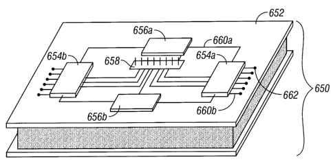
In an alternate embodiment, the backplate 608 (Figure 7) is eliminated and the
PC carrier
itself makes up the backplate. Figures 8A and 8B depict such a display device
650. As can be
seen in Figure 8A, which depicts device 650 in an assembled state, carrier 652
provides physical
support for driver chips 652a and 652b, which are in electrical connection
with electronic
components 656a and 656b and external interconnect pins 658 via trace leads
660a, which may
be located on or within carrier 652. Driver chips 654a,b are also in
electrical connection with
electrical feedthroughs 662 via trace leads 660b.
As can be seen in Figure 8B, which depicts device 650 in an exploded view,
electrical
feedthroughs 662 extend from the upper surface of carrier 652 to the lower
surface. When
assembled, anisotropic conducting film ledge 664 provides an electrical
connection between
feedthroughs 662 and trace leads 660c located on the upper surface of
transparent substrate 666.
Trace leads 660c are in electrical contact with array 668 of interferometric
modulators located on
the upper surface of transparent substrate 666, enabling an electrical
connection between driver
chips 654a,b and array 668. When device 650 is assembled, seal ring 670 forms,
along with
transparent substrate 666 and carrier 652, a protective cavity around array
668. Thus, a carrier
such as carrier 652 provides a means for supporting electronic circuitry, such
as driver circuitry,
and for protecting the array 668.
ACF materials are conveniently employed for providing electrical interconnects
between
components, and they are often used to connect the flex connector of TAB
drivers to display
substrates. However, other connection methods can be employed, including but
not limited to
zebra connectors, flex cables, bump bonds, and micromechanical pressure
conductors (e.g.
MEMS springs), which are described in greater detail with respect to Figure l
OB.
In certain embodiments in which the interferometric modulator carrier 652 is
formed
from materials through which vapor can permeate into the protective cavity,
the interior side of
interferometric modulator carrier 652 may be advantageously coated with a
vapor barrier 672. In
addition to, or in place of, vapor barrier 672, desiccant 674 may be provided
within the protective
cavity. In Figure 8B, a layer of desiccant 674 is shown below the vapor
barrier 672. In
embodiments in which the interferometric modulator carrier 652 is made of a
substrate that is
sufficiently vapor resistant, no vapor barrier 672 is required.
Figures 9A and 9B depict a top view of two components, 700 and 702 that come
together
to make a display device similar to the device 650 shown in Figure 8. Figure
9A depicts the lower
portion 700 of the two components which come together to make the display
device. A
transparent lower substrate 704 includes an interferometric modulator array
706 which is
-16-
CA 02513030 2005-07-22
configured to reflect light through the substrate 704. Surrounding the outer
edges of the substrate
704 and circumscribing a seal ring 708 is an ACF ledge 710 which provides
electrical
connections to the array 706 via trace leads 712a located on substrate 704.
Figure 9B depicts a top view of the upper portion 702 which is configured to
mate with
the lower portion 700 and come together to make the display device. A
corresponding
interconnect ledge 714, located along the edge of this interferometric
modulator carrier 716,
circumscribes a set of electronic components 718a-d (e.g. driver chips, ICs,
passives, etc.), at
least some of which (718a,b in this embodiment) are electrically connected to
interconnect ledge
714 via trace leads 712b. Some of electronic components 718a-d are connected
to each other via
trace leads 712c, and connections between some electronic components 718 and
external
circuitry can be made via trace leads 712 and external interconnect pins 720.
When the two
modules are brought together, the connection between interconnect ledge 714
and ACF ledge 710
places electronic components 718a,b in electrical connection with the array
706 located on
substrate 704.
Figures 10A and lOB depict a reduced footprint display device 750. As will be
apparent
from the following discussion, the reduced footprint of device 750 is due to
the elimination of
ledges, such as those seen in Figures 7 and 8, on which components such as
driver chips and
connections were located, exterior to the protective cavity formed by the seal
rings. Figure 10A
shows the device 750 in an assembled state, and Figure lOB shows the device
750 in an exploded
view. Referring to Figure 10A the device 750 includes a transparent substrate
754 which is
sealed to an interferometric modulator carrier 770 through a seal ring 764. In
this embodiment,
the carrier 770 acts as a backplate for the device 750.
The carrier 770 includes a first display circuit 756 which connects through a
trace lead
762a to an electrical feedthrough 766. The electrical feedthrough 766 is used
as a connection to
the interior components of the device 750 as will be explained in more detail
with reference to
Figure 10B. The display circuit 756 is also in electrical connection with a
set of external
interconnect pins 760 for connecting the display device 750 to external
devices. In addition, a
set of interconnect leads 762b connect the display circuit 756 to a flex cable
772 which provide
an electrical connection to the interior components of the device 750.
Referring now to Figure 10B, the interior components of the reduced footprint
display
device 750 can be seen. As shown, the transparent substrate 754 includes an
interferometric
modulator array 752 that is configured to reflect light through the substrate
754. Interior to the
interferometric modulator array 752 are a set of conducting posts 768 which
are adapted to
provide an electrical connection to a matching set of conducting pads 767a on
the lower surface
of the carrier 770. As will be imagined, the conducting pads 767a are in
communication with the
-17-
CA 02513030 2005-07-22
electrical feedthroughs 766 so as to provide an electrical link to the display
circuit 756 (Figure
IOA).
Of course it should be realized that the display circuit 756 can be connected
to the
conducting pads 767 through the flex cable 772. As shown, the flex cable 772
mounts to the
lower surface of the carrier 770 and is in electrical connection with the
conducting pads 767b,
which then connect to the interferometric modulator 752 through the conducting
posts 768. This
configuration does not require feedthroughs to be present in the carrier 770
and thus can reduce
the chance that water vapor may traverse the carrier 770 and come in contact
with the
interferometric modulator 752.
Also shown is a desiccant 774 on the lower surface of the carrier 770 which
acts to
absorb any moisture that may enter the protective cavity of the device.
Because contacts between the conducting posts 768 and the conducting pads
767a,b are
internal to the device 750, the material characteristics of the bonds can
present issues. ACF
materials, which outgas during curing, can produce substances that interfere
with the operation of
the array. Alternatives to ACF materials include low temperature solders,
micromechanical
pressure connectors, bump bonds, and other affixing materials which are
neutral from a chemical
and outgassing standpoint. In some embodiments, such as those employing vacuum
packaging,
the electrical feedthroughs can act as both interconnects and mechanical
standoffs, or just
mechanical standoffs. As mechanical standoffs, they maintain a distance
between the
interferometric modulator array and the interferometric modulator backplate to
protect against the
force of external mechanical or atmospheric pressures.
Of course, while only a relatively few conducting posts are illustrated in
this
embodiment, it should be realized that tens, hundreds, or thousands of such
posts can be
fabricated within the array 752. Similarly, tens, hundreds or thousands of
matching conducting
pads can be formed on the lower surface of the carrier 770. This allows
complex electronic
circuits, such as driver circuits to be connected to the array 752.
While Figure 10 depicts an embodiment using conducting support posts, a
variety of
structures can be utilized to place the array 752 in electrical connection
with the interferometric
modulator carrier 770. For instance, micromechanical pressure connectors can
be used.
Micromechanical pressure connectors come in a variety of forms, and include
conductive
metallic structures that extend above the plane of the substrate because of
inherent mechanical
stresses. They can be fingers or coils which when deposited and patterned
reside partially on a
sacrificial layer and partially on the substrate or on one or more films or
structures without an
intervening sacrificial layer between it and the structure. In this
embodiment, during the final
MEMS fabrication step (the release step where the sacrificial layer is
removed), the stresses in
the connector cause it to displace vertically away from the substrate. If
aligned properly with
-18-
CA 02513030 2005-07-22
conducting features on an opposing substrate or interferometric modulator
carrier, they can
provide an electrical interconnect which does not outgas.
It should also be understood that some or all of the driver chips could be
placed on the
lower surface of the carrier 770 and thereby inside of the sealed cavity
formed by the carrier 770,
the transparent substrate 754 and the seal ring 764. In this alternate
embodiment, as illustrated in
Figure l OB, a circuit chip 758 is mounted on the lower surface of the carrier
770. The chip 758 is
in electrical communication with the flex cable 772 via traces 762c and the
conducting pads 767b
via traces 762d. This allows the chip 758 to communicate with the
interferometric modulator
array 752 and to the display circuit 756 which is on the upper surface of the
carrier 770.
Figure 11 depicts an embodiment of a display module 800 in which driver chips
802a and
802b are located on a transparent substrate 804, and are electrically
connected via trace leads
810a to an interferometric modulator array 806, so that the driver chips
802a,b can control the
state of the array 806. The driver chips 802a,b are located within a
protective cavity formed
when the substrate 804 is bonded to interferometric modulator carrier 814 by
seal ring 816. The
driver chips 802a,b are electrically connected to external interconnect pins
808 via trace leads
810b and 810c, as well as flex cable 812. A configuration in which the driver
chips 802a,b are
located on the same surface as the array 806 may advantageously reduce the
number of
connections to be made with the interferometric modulator carrier 814, as a
driver chip suitable
for use in this display may have significantly more outputs than inputs.
Although not depicted, a vapor barrier and/or desiccant can be used on the
interior of the
protective cavity formed by at least seal ring 816, carrier 814, and substrate
804. Additional
components (not shown), including but not limited to those components
previously discussed
with respect to other embodiments, can be incorporated into display module
800, either on the
transparent substrate 804 or on interferometric modulator carrier 814. These
components can be
internal or external to the protective cavity formed by substrate 804, carrier
814, and seal ring
816, and connections with and between these components can be made using any
of the methods
discussed above with respect to previous embodiments.
Dual Sided Displays
A class of electronic products employs two displays integrated opposite each
other so
that there are two viewable surfaces on opposing sides. This class includes
"clamshell" phones,
which can have a main display which acts as the primary information interface
and is revealed
only when the product is opened, and a sub-display, which resides on the
exterior of the product
and provides status information at all times. These phones make aggressive
demands on product
integration and display module thinness.
-19-
CA 02513030 2005-07-22
Figure 12 illustrates dual-sided interferometric modulator based sub-
display/main-display
module 850. As shown, interferometric modulator array 852 resides on
transparent substrate 854
and is bonded via seal ring 856 to interferometric modulator carrier 858. The
carrier, 858, is
subsequently bonded via seal ring 860 to transparent substrate 862, upon which
interferometric
modulator array 864 resides. In this particular configuration, the thickness
of the overall module
850 is reduced because the two displays share the same carrier 858, which can
perform one or
more of the functions previously described. Therefore, in certain embodiments,
the carrier 858
provides a means for supporting electronic circuitry configured to control the
state of array 864.
Although the carrier 858 and each of the substrates 854 or 862 are depicted in
Figure 12
as being the same size, the carrier and/or either of the substrates can extend
beyond either of seal
rings 856 and 860, and additional components may be located on either of these
surfaces external
to the seal rings. Thus, the surface area of any one of the carrier 858 or
substrates 854 or 862
may be greater than the surface areas of the others. Connections between the
interferometric
modulators 852 and 864 and the carrier 858, as well as connections through the
carrier, can be
made via any method or combination of methods discussed previously, including
but not limited
to flex cables, electrical feedthroughs, trace leads, conductive support
posts, or micromechanical
pressure connectors.
Another embodiment of a dual sided display 900 is shown in Figure 13. In this
embodiment the interferometric modulator carrier has been eliminated. An upper
transparent
substrate 902, bearing an upper interferometric modulator array 906 is bonded
via a seal ring 910
to a lower transparent substrate 908 on its opposing side. Lower transparent
substrate 904 bears a
lower interferometric modulator array 908 and is configured to reflect light
through the lower
transparent substrate 904. Because the upper interferometric modulator array
906 (which acts as
the sub-display) is smaller in size than the lower interferometric array 908,
additional area
remains on the inner surface of upper transparent substrate 902 which may be
used to support
various functions that the interferometric modulator carrier would typically
support in other
embodiments. Thus, in certain embodiments, upper substrate 902 provides a
means for
supporting electronic circuitry configured to control the state of array 906.
In this embodiment,
upper transparent substrate 902 can be formed of a polymeric substance which
is less vapor
resistant than glass. In order to prevent moisture buildup over the lifetime
of the device, vapor
barrier 912 and desiccant 914 are provided on the inner surface of substrate
902.
In other embodiments of the display 900 depicted in Figure 13, wherein
electronic
components such as ICs are located within the protective cavity formed by the
upper and lower
transparent substrates, the vapor barrier 912 and/or desiccant 914 may be
applied directly or
-20-
CA 02513030 2005-07-22
indirectly over the electronic components. This application may be done by
spray-coating or
screen printing, for example, or by any other suitable method.
Figure 14 illustrates another embodiment of a dual sided display 950, wherein
an upper
transparent substrate 952 and interferometric modulator array 954 act as the
sub-display. In this
S embodiment, they are bonded and attached to an annular interferometric
modulator carrier 956.
This assembly is then bonded via a seal ring 958, to a transparent substrate
960 that is configured
to pass light to an interferometric modulator array 962. As can be seen, the
surface area of the
substrate 952 is less than the surface area of the substrate 960. When
necessary (e.g. when the
annular carrier 956 comprises plastic, which is less vapor resistant than
glass), a vapor barrier
964 and desiccant 966 may be provided.
While the module configuration shown in Figure 14 may not be as thin as that
illustrated
in Figure 13, it provides a greater degree of flexibility in the features that
can be incorporated in
the sub-display carrier plane of the module. Because carrier 956 need not be
transparent, the
material used can be selected based on other considerations, such as strength.
Electrical
feedthroughs can be more easily provided through carrier 956 by passing them
along the juncture
between the transparent substrate 952 and the PC carrier 956. This enables
placement of driver
chips or other components on the upper surface of the carrier 956. Because of
the height of the
transparent substrate 952, components such as driver chip 968 which have
heights equal to or less
than the height of the substrate 952 will not add to the overall height of the
device 950. Trace
leads 970 can run, for example, from the driver chip 968 located on the upper
surface of the
substrate 956 directly to the array 954, without the need for flex cables,
feedthroughs, or other
complex connections. Because carrier 956 can be a multilayer conductor polymer
laminate, as
discussed previously, leads 970 can run within the carrier 956, advantageously
protecting the lead
from damage. Leads 970 may advantageously comprise two leads, one on or within
Garner 956
and placed in electrical contact with another lead on the lower surface of
upper substrate 952.
Still another embodiment of a dual sided display 1000 is shown in Figure 15.
Components depicted in Figure 1 S include an upper transparent substrate 1002
bearing an
interferometric modulator array 1006 configured to reflect light through the
transparent substrate
1002. The upper transparent substrate 1002 is bonded via a sealing bead 1010
to a lower
transparent substrate 1004, on which interferometric modulator arrays 1008 is
located.
Figure 16 illustrates an embodiment of a device 1150 (e.g. a cellular phone)
comprising
an interferometric modulator carrier 1152, which is bonded to a transparent
substrate 1154 by
means of a seal ring 1156. As can be seen from Figure 16, the surface area of
carrier 1152 is
larger than the surface area of substrate 1154. Driver chip 1158 is located on
the upper side of
carrier 1152, and electrically connected via electrical feedthrough 1160 and
conducting post 1162
-21-
CA 02513030 2005-07-22
to an array 1164 of interferometric modulators located on substrate 1154 and
configured to reflect
light through substrate 1154. Located on the same side of the carrier 1152 as
the driver chip
1158 and in electrical connection with driver chip 1158 via trace leads 1166
are antenna 1168,
device processor/memory 1170, battery 1172 and external interconnect hardware
1174. Located
on the opposite side of the carrier 1152 as the driver chip 1158 are the
keyboard, keyboard
lighting, and microphone hardware, referenced collectively as 1176. Although
not shown, the
keyboard and microphone hardware 1176 may be placed in electrical connection
with the driver
chip 1158 on the opposite side of the carrier 1152 by any suitable method,
including but not
limited to electrical feedthroughs, trace leads, and flex cables of the types
discussed above.
As illustrated in Figure 16, carrier 1152 for the interferometric modulator
1164 is the
primary internal structural component while also acting as the electrical
interconnect means.
This entire assembly is encased in a shell 1166 which need not have the
structural rigidity of
shells used in products which isolate the display. The construction of this
shell and its
connection to the interferometric modulator carrier minimize the amplitude of
mechanical shocks
transmitted to the transparent substrate 1154 and associate components,
thereby increasing the
product's overall ruggedness. Carrier 1152 thus becomes the "backbone" of the
device.
In contrast with conventional display-centric device assembly methods, in
which the
strength of the device comes from the case encapsulating the device, the
strength of the device
can come instead from the carrier 1152 located within the device, as the
carrier serves as the
primary structural component of the device. The increased strength of the
carrier 1152 may be a
result of the materials which comprise the carrier. Alternately or in addition
to the choice of
materials, the strength of the carrier may be the result of the dimensions of
the carrier. For
instance, increasing the thickness of the carrier 1152 or modifying the cross-
sectional shape of
the carrier can provide the strength necessary for the carrier to function as
a primary structural
component of the device 1150. Many other configurations are possible with this
technique that
increases both the physical and structural role the interferometric modulator
carrier plays in the
product.
Figures 18A and 18B are system block diagrams illustrating another embodiment
of a
display device 2040. The display device 2040 can be, for example, a cellular
or mobile
telephone. However, the same components of display device 2040 or slight
variations thereof are
also illustrative of various types of display devices such as televisions and
portable media
players.
The display device 2040 includes a housing 2041, a display 2030, an antenna
2043, a
speaker 2045, an input device 2048, and a microphone 2046. The housing 2041 is
generally
formed from any of a variety of manufacturing processes as are well known to
those of skill in
-22-
CA 02513030 2005-07-22
the art, including injection molding, and vacuum forming. In addition, the
housing 2041 may be
made from any of a variety of materials, including but not limited to plastic,
metal, glass, rubber,
and ceramic, or a combination thereof. In one embodiment the housing 2041
includes removable
portions (not shown) that may be interchanged with other removable portions of
different color,
S or containing different logos, pictures, or symbols.
The display 2030 of exemplary display device 2040 may be any of a variety of
displays,
including a bi-stable display, as described herein. In other embodiments, the
display 2030
includes a flat-panel display, such as plasma, EL, OLED, STN LCD, or TFT LCD
as described
above, or a non-flat-panel display, such as a CRT or other tube device, as is
well known to those
of skill in the art. However, for purposes of describing the present
embodiment, the display 2030
includes an interferometric modulator display, as described herein.
The components of one embodiment of exemplary display device 2040 are
schematically
illustrated in Figure 18B. The illustrated exemplary display device 2040
includes a housing 2041
and can include additional components at least partially enclosed therein. For
example, in one
embodiment, the exemplary display device 2040 includes a network interface
2027 that includes
an antenna 2043 which is coupled to a transceiver 2047. The transceiver 2047
is connected to the
processor 2021, which is connected to conditioning hardware 2052. The
conditioning hardware
2052 may be configured to condition a signal (e.g. filter a signal). The
conditioning hardware
2052 is connected to a speaker 2045 and a microphone 2046. The processor 2021
is also
connected to an input device 2048 and a driver controller 2029. The driver
controller 2029 is
coupled to a frame buffer 2028 and to the array driver 2022, which in turn is
coupled to a display
array 2030. A power supply 2050 provides power to all components as required
by the particular
exemplary display device 2040 design.
The network interface 2027 includes the antenna 2043 and the transceiver 2047
so that
the exemplary display device 2040 can communicate with one or more devices
over a network.
In one embodiment the network interface 2027 may also have some processing
capabilities to
relieve requirements of the processor 2021. The antenna 2043 is any antenna
known to those of
skill in the art for transmitting and receiving signals. In one embodiment,
the antenna transmits
and receives RF signals according to the IEEE 802.11 standard, including IEEE
802.11(a), (b), or
(g). In another embodiment, the antenna transmits and receives RF signals
according to the
BLUETOOTH standard. In the case of a cellular telephone, the antenna is
designed to receive
CDMA, GSM, AMPS or other known signals that are used to communicate within a
wireless cell
phone network. The transceiver 2047 pre-processes the signals received from
the antenna 2043
so that they may be received by and further manipulated by the processor 2021.
The transceiver
-23-
CA 02513030 2005-07-22
2047 also processes signals received from the processor 2021 so that they may
be transmitted
from the exemplary display device 2040 via the antenna 2043.
In an alternative embodiment, the transceiver 2047 can be replaced by a
receiver. In yet
another alternative embodiment, network interface 2027 can be replaced by an
image source,
which can store or generate image data to be sent to the processor 2021. For
example, the image
source can be a digital video disc (DVD) or a hard-disc drive that contains
image data, or a
software module that generates image data.
Processor 2021 generally controls the overall operation of the exemplary
display device
2040. The processor 2021 receives data, such as compressed image data from the
network
interface 2027 or an image source, and processes the data into raw image data
or into a format
that is readily processed into raw image data. The processor 2021 then sends
the processed data
to the driver controller 2029 or to frame buffer 2028 for storage. Raw data
typically refers to the
information that identifies the image characteristics at each location within
an image. For
example, such image characteristics can include color, saturation, and gray-
scale level.
In one embodiment, the processor 2021 includes a microcontroller, CPU, or
logic unit to
control operation of the exemplary display device 2040. Conditioning hardware
2052 generally
includes amplifiers and filters for transmitting signals to the speaker 2045,
and for receiving
signals from the microphone 2046. Conditioning hardware 2052 may be discrete
components
within the exemplary display device 2040, or may be incorporated within the
processor 2021 or
other components.
The driver controller 2029 takes the raw image data generated by the processor
2021
either directly from the processor 2021 or from the frame buffer 2028 and
reformats the raw
image data appropriately for high speed transmission to the array driver 2022.
Specifically, the
driver controller 2029 reformats the raw image data into a data flow having a
raster-like format,
such that it has a time order suitable for scanning across the display array
2030. Then the driver
controller 2029 sends the formatted information to the array driver 2022.
Although a driver
controller 2029, such as a LCD controller, is often associated with the system
processor 2021 as a
stand-alone Integrated Circuit (IC), such controllers may be implemented in
many ways. They
may be embedded in the processor 2021 as hardware, embedded in the processor
2021 as
software, or fully integrated in hardware with the array driver 2022.
Typically, the array driver 2022 receives the formatted information from the
driver
controller 2029 and reformats the video data into a parallel set of waveforms
that are applied
many times per second to the hundreds and sometimes thousands of leads coming
from the
display's x-y matrix of pixels.
-24-
CA 02513030 2005-07-22
In one embodiment, the driver controller 2029, array driver 2022, and display
array 2030
are appropriate for any of the types of displays described herein. For
example, in one
embodiment, driver controller 2029 is a conventional display controller or a
bi-stable display
controller (e.g., an interferometric modulator controller). In another
embodiment, array driver
S 2022 is a conventional driver or a bi-stable display driver (e.g., an
interferometric modulator
display). In one embodiment, a driver controller 2029 is integrated with the
array driver 2022.
Such an embodiment is common in highly integrated systems such as cellular
phones, watches,
and other small area displays. In yet another embodiment, display array 2030
is a typical display
array or a bi-stable display array (e.g., a display including an array of
interferometric
modulators).
The input device 2048 allows a user to control the operation of the exemplary
display
device 2040. In one embodiment, input device 2048 includes a keypad, such as a
QWERTY
keyboard or a telephone keypad, a button, a switch, a touch-sensitive screen,
a pressure- or heat-
sensitive membrane. In one embodiment, the microphone 2046 is an input device
for the
exemplary display device 2040. When the microphone 2046 is used to input data
to the device,
voice commands may be provided by a user for controlling operations of the
exemplary display
device 2040.
Power supply 2050 can include a variety of energy storage devices as are well
known in
the art. For example, in one embodiment, power supply 2050 is a rechargeable
battery, such as a
nickel-cadmium battery or a lithium ion battery. In another embodiment, power
supply 2050 is a
renewable energy source, a capacitor, or a solar cell, including a plastic
solar cell, and solar-cell
paint. In another embodiment, power supply 2050 is configured to receive power
from a wall
outlet.
In some implementations control programmability resides, as described above,
in a driver
controller which can be located in several places in the electronic display
system. In some cases
control programmability resides in the array driver 2022. Those of skill in
the art will recognize
that the above-described optimization may be implemented in any number of
hardware and/or
software components and in various configurations.
Contoured Backplates
In yet another exemplary embodiment, the backplate comprises a shaped printed
circuit
board or other shaped interferometric modulator carrier. Figures 17A and 17B
depict an
embodiment of a device 1200 comprising a shaped backplate 1228. As can be seen
in Figure
17A, the backplate 1228 has a central region 1230 that is domed. This domed
central region
1230 is surrounded by a perimeter region 1226 that is substantially flatter.
-25-
CA 02513030 2005-07-22
In the embodiment of Figures 17A and 17B, the backplate 1228 comprises a
printed
circuit board (PCB). This printed circuit board is curved such that a cavity
1250 (see Figure 17B)
within the device 1200 is sufficiently large to accommodate an array 1210 of
modulators housed
therein. In embodiments using a PCB for the backplate 1228, the shaped cavity
1250 may be
formed by stamping the PCB backplate 1228 or any other suitable method for
shaping or cutting
a PCB. In alternate embodiments, the backplate 1228 may comprise glass or a
glass compound,
which is substantially impermeable to moisture. If made of glass, the shaped
central region 1230
of the backplate may be formed by sandblasting or any other suitable glass
shaping or cutting
method.
In the embodiment shown in Figure 17A, an electrical component 1260 is mounted
to the
backplate 1228. A set of trace leads 1240 extend from holes 1234 in a
perimeter region 1226 of
the backplate 1228 and are electrically connected to the electrical component
1260. Leads 1262
from the electrical component 1260 may, for example, be soldered to the trace
leads 1240. As
will be discussed further with respect to Figure 17B, the holes 1234 comprise
vias 1242 which
enable an electrical connection to be made between the upper and lower
surfaces of backplate
1228. In one exemplary embodiment, the electrical component 1260 is a driver
chip that is
configured to control the state of modulators in the array 1210. In other
embodiments, the
electrical component could be any variety of electrical components or devices,
including but not
limited to other integrated circuits, other passive and active electrical
structures or components,
or other surface-mounted electronics such as transistors, capacitors,
resistors, diodes, inductors,
etc.
Now with respect to Figure 17B, it can be seen that attaching the backplate
1228 to a
substrate 1216 forms a cavity 1250 in the package structure 1200. The array
1210 of modulators
is housed in this cavity 1250 between the backplate 1228 and the substrate
1216. As described
above, the backplate 1228 is domed. The curvature of the domed central region
1230 also
produces a recess 1252 where the distance between the backplate 1228 and the
substrate 1216 is
greater than in other parts of the cavity 1250. The cavity 1250 is thus
advantageously enlarged in
the central region 1230 where the array 1210 of modulators is disposed.
Room for unimpeded operation of the modulators the array 1210 is thereby
provided.
Although the central region 1230 of the backplate 1228 is depicted as domed,
numerous other
shapes are also within the scope of the invention. For example, the backplate
1228 may have a
curved or recessed shape that is not necessarily limited to the central region
1230 or may have
other shapes such as a ribbed design or a raised rectangular design. In one
embodiment, the
edges of the backplate 1228 are beveled so that they provide a lower profile.
As long as at least a
portion of the modulators in the array 1210 are within an enlarged region or
cavity of the
-26-
CA 02513030 2005-07-22
backplate 1228, then the desired room for unimpeded operation of the that
portion of the array
1210 is provided.
A plurality of through holes 1234 are formed in the perimeter region 1226. The
holes
1234 are staggered in the embodiment shown in Figure 17B. Separation between
alternating
holes 1234 may be between about 50 to 75 micrometers in some designs. In other
embodiments,
wherein the holes 1234 are not staggered, the pitch may also be between about
75 to 125
micrometers (pm). The backplate 1228 may have a thickness of between about 0.5
and 2.0
millimeters (mm) and thus the through holes will also be the same depth so as
to penetrate
completely through the backplate 1228. Values outside these ranges, however,
are also within
the scope of the invention.
The number and configuration of holes 1234 can vary in different embodiments
of the
invention. For example, in one embodiment the holes 1234 may be in the domed
or recessed
central region 1230 of the backplate 1228. Placement of the holes 1234 will
depend on the
specific functionality desired. The exact position, and combinations of
positions, of the holes
1234, are within the skill in the art. The holes 1234 may be formed by
mechanically drilling,
laser drilling, or ultrasonic drilling, for example. Other standard methods of
forming the holes
1234 rnay also be employed.
Figure 17B also shows the electrical traces 1240 disposed on, and traversing,
the printed
circuit board backplate 1228. An electrical connection is formed between the
backplate 1228 and
the spatial modulator, as described above (see Figure 17A). For example, in
the embodiment
shown, the electrical traces 1240 contact vias 1242 that pass through the
printed circuit board
backplate 1228. The vias 1242 may be, for example, plated vias fabricated in
any manner well
known in the printed circuit board field. Solder 1244 between the vias 1242
and a set of
electrical pads 1246 on the substrate 1216 provides a conductive pathway
therebetween. As a
result of these electrical connections, the electrical traces 1240 on the PCB
backplate 1228 are in
electrical communication with the electrodes in the array 1210 of modulators.
As described
above, a wide variation in the designs of and processes for fabricating the
electrical connection
between the PCB backplate 1228 the modulator array 1210 are possible.
As illustrated in 17B, the PCB backplate 1228 may comprise a multilayer
structure. For
example, a metallization layer 1264 can be embedded in the printed circuit
board backplate 1228.
This metallization layer 1264 is electrically connected to one of the traces
1240 by a conducting
plug 1266 as is conventional in multilayer printed circuit boards. Other
approaches to
manufacturing a multilayered backplane may be employed. Additional conductive
paths may be
provided in this manner. For example, in one exemplary embodiment (not
depicted) the electrical
traces may be an integral part of the PCB backplate. In this embodiment, the
electrical traces
-27-
CA 02513030 2005-07-22
may be embedded in the PCB backplate by conventional multilayering of the PCB
backplate
1228. These electrical traces can be configured in many ways, including, but
not limited to, the
electrical traces being in electrical communication vias and/or the electrical
pads. In addition, the
electrical traces 1240 can be in electrical communication with individual
modulators or in direct
electrical communication with the entire array or subportions thereof.
In the embodiment depicted in Figure 17B, a desiccant 1254 is positioned
between the
array 1210 of optical modulators and the backplate 1228. The recessed portion
of the backplate
1228 offers increased clearance for the desiccant 1254 to be disposed in the
cavity 1250 without
interfering with the operation of the array 1210.
The desiccant 1254 may have different shapes, forms, and sizes and may be
applied in
different ways. In the embodiment shown in Figure 17B, this desiccant 1254
comprises a sheet
that is mounted to the backplate 1228 with adhesive. Specifically, the
desiccant 1254 is adhered
to the central region 1230 of the backplate 1228. Advantageously, the recess
created by the
curvature of the front side of the backplate 1228 provides space for the
desiccant 1254 above the
modulator array 1210.
The package structure 1200 enhances performance of the modulators in multiple
ways as
well. Integration of electrical busses 1240 on the outside of the package
structure 1200 offer a
wide range of design possibilities that may enable enhancements of the
performance of the array
1210 or provide additional features. For example, electrical busses can be
arranged such that one
end of the bus connects to one end of a row or column electrode within the
array, and the other
end of the bus connects to the other end of the same row or column electrode.
This connection
adds a parallel conduction path to the row or column, reducing the overall
resistance of the row
or column.
Advantageously, the conductive busses 1240 provide a relatively high
conductivity
connection to the array 1210 of optical modulators. The conductive busses 1240
can be
fabricated with larger dimensions (e.g., width and thickness) than the
electrodes that connect the
modulators in the array 1210. This enhanced conductivity and, thus, reduced
impedance, allows
the optical modulators in the array 1210 to be driven faster. In addition,
since the conductive
busses 1240 are outside of the package if they are mounted on the outer
surface 1232 of the
package structure 1200, precious real estate within the cavity 1250 where the
array 1210 of
modulators is located, is not sacrificed. Interference with the mechanical
operation of the array
1210 of interferometric modulators is also avoided. The package structure 1200
may also afford
other advantages are not specifically recited herein.
Other configurations of the conductive busses 1240 may be utilized in other
embodiments. For example, the conductive busses 1240 may follow different
pathways and may
-28-
CA 02513030 2005-07-22
be connected differently. The specific geometry may be altered depending on
the designs or
desired function. For example, in one exemplary embodiment (not depicted), a
portion of the
holes 1234 are placed on the domed region 1230 of the backplate 1228 and the
conductive busses
1240 are in electrical communication with at least a portion of the modulators
in the array 1210
that are below the respective holes 1234. This embodiment may be useful for
performing testing
on certain portions of the array 1210.
While the above detailed description has shown, described, and pointed out
novel
features of the invention as applied to various embodiments, it will be
understood that various
omissions, substitutions, and changes in the form and details of the device or
process illustrated
may be made by those skilled in the art without departing from the spirit of
the invention. As will
be recognized, the present invention may be embodied within a form that does
not provide all of
the features and benefits set forth herein, as some features may be used or
practiced separately
from others.
-29-