Note: Descriptions are shown in the official language in which they were submitted.
CA 02513384 2012-05-22
78625-26
ELECTRICAL TRANSFORMER
TECHNICAL FIELD
This invention relates to electrical transformers, and more particularly to
compact
electrical transformers.
BACKGROUND
As is known in the art, electrical transformers have a wide variety of
applications.
The transformer includes a primary winding and an adjacent secondary winding.
Changes in
electrical current passing through the primary winding induce a corresponding
cnange in a
magnetic field around the primary winding. This changing magnetic field
induces a
corresponding change in current in the adjacent, magnetically coupled
secondary winding.
As is also known in the art, it is desirable to reduce the size of the
transformer.
SUMMARY
In accordance with an aspect of the present invention, an electrical
transformer is provided
having a first dielectric. The first dielectric includes a plurality of first
electrically isolated electrical
conductor segments. A second dielectric is disposed over, and in registration
with, the first
dielectric, such second dielectric having a plurality of second electrically
isolated electrical
conductor segments disposed on the second dielectric. The transformer includes
a core
having an aperture therein, such aperture extending between the first and
second dielectrics.
A plurality of third electrically isolated electrical conductor segments is
provided. First ends
of the third electrically isolated electrical conductor segments are
electrically connected to
the plurality of first electrically isolated electrical conductor segments and
second ends of the
third electrically isolated electrical conductor segments are electrically
connected to the
plurality of second electrically isolated electrical conductor segments to
provide a portion of
a primary winding and a portion of a secondary winding for the transformer.
The primary
winding comprises first ones of the first electrically isolated electrical
conductor segments,
first ones of the second electrically isolated electrical conductor segments,
and first ones of
the third electrically isolated electrical conductor segments. The secondary
winding
comprises second ones of the first electrically isolated electrical conductor
segments, second
1
CA 02513384 2005-07-13
WO 2004/072997 PCT/US2004/002465
ones of the second electrically isolated electrical conductor segments, and
second ones of the
third electrically isolated electrical conductor segments.
In one embodiment, the first and second dielectrics comprise multilevel
printed
circuit boards.
In one embodiment, the first and second multilevel printed circuit boards are
disposed
in a pair of overlaying planes and the plurality of third electrically
isolated electrical
conductor segments are disposed perpendicular to the overlaying planes.
In one embodiment, the primary and secondary winding provide loops around the
core.
In one embodiment, the third electrically isolated electrical conductor
segments are
embedded within the core.
In one embodiment, the core comprises a toroidal shaped body and the
dielectric body
is disposed in a central region of the toroidal shaped body.
In accordance with another feature of the invention, an electrical transformer
is
provided having a first multilayer printed circuit board. The first multilevel
printed circuit
board includes a plurality of first electrically isolated electrical conductor
segments disposed
on each one of a plurality of electrically isolated levels of such first
multilevel printed circuit
board. A second multilayer printed circuit board is, disposed over, and in
registration with,
the first multilevel printed circuit board. The second multilevel printed
circuit board has a
plurality of second electrically isolated electrical conductor segments
disposed on each one
of a plurality of electrically isolated levels of such second multilevel
printed circuit board. A
pair of dielectric bodies is disposed between the first multilevel printed
circuit board and the
second multilevel printed circuit board. Each one of such bodies has disposed
therein a
plurality of third electrically isolated electrical conductor segments. First
ends of the third
electrically isolated electrical conductor segments are electrically connected
to the plurality
of first electrically isolated electrical conductor segments and second ends
of the third
electrically isolated electrical conductor segments are electrically connected
to the plurality
of second electrically isolated electrical conductor segments to provide a
primary winding
and a secondary winding for the transformer. The primary winding comprises a
first ones of
the first electrically isolated electrical conductor segments, first ones of
the second
electrically isolated electrical conductor segments, and first ones of the
third electrically
isolated electrical conductor segments. The secondary winding comprises second
ones of the
2
CA 02513384 2005-07-13
WO 2004/072997 PCT/US2004/002465
first electrically isolated electrical conductor segments, second ones of the
second electrically
isolated electrical conductor segments, and second ones of the third
electrically isolated
electrical conductor segments.
In accordance with another feature of the invention, an electrical transformer
structure
is provided. The structure includes a first multilayer printed circuit board
having a plurality
of first electrically isolated electrical conductor segments disposed on each
one of a plurality
of electrically isolated levels of such first multilevel printed circuit
board. The structure
includes a second multilayer printed circuit board, disposed over, and in
registration with, the
first multilevel printed circuit board. The second multilevel printed circuit
board has a
plurality of second electrically isolated electrical conductor segments
disposed on each one
of a plurality of electrically isolated levels of such second multilevel
printed circuit board. A
dielectric spacer member is disposed between the first multilevel printed
circuit board and
the second multilevel printed circuit board. The spacer member has a plurality
of apertures
therethrough. The apertures in the spacer member pass between a top and a
bottom surface
of the spacer member. A plurality of toroidal shaped cores is provided. Each
one of such
cores is disposed in a corresponding one of the plurality of apertures of the
dielectric spacer
member. Each one of the cores has an aperture therein, the apertures of the
cores being
coaxial with the apertures in the dielectric spacer member. A plurality of
dielectric bodies is
provided. Each one of such dielectric bodies is disposed in a corresponding
one of the
apertures in the cores. A plurality of plurality of dielectric bodies has a
corresponding one of
the sets of third electrically isolated electrical conductor segments. First
ends of the third
electrically isolated electrical conductor segments are electrically connected
to the plurality
of first electrically isolated electrical conductor segments and second ends
of the third
electrically isolated electrical conductor segments are electrically connected
to the plurality
of second electrically isolated electrical conductor segments to provide a
primary winding
and a secondary winding for the transformer. The primary winding comprises
first ones of
the first electrically isolated electrical conductor segments, first ones of
the second
electrically isolated electrical conductor segments, and first ones of the
third electrically
isolated electrical conductor segments. The secondary winding comprises second
ones of the
first electrically isolated electrical conductor segments, second ones of the
second electrically
isolated electrical conductor segments, and second ones of the third
electrically isolated
electrical conductor segments.
3
CA 02513384 2012-05-22
78625-26
According to another aspect of the invention, there is provided an
electrical transformer, comprising: a first multilayer printed circuit board
having a
plurality of first electrically isolated electrical conductor segments
disposed on each
one of a plurality of electrically isolated levels of such first multilevel
printed circuit
board; a second multilayer printed circuit board, disposed over, and in
registration
with, the first multilevel printed circuit board, such second multilevel
printed circuit
board having a plurality of second electrically isolated electrical conductor
segments
disposed on each one of a plurality of electrically isolated levels of such
second
multilevel printed circuit board; a core having an aperture therein, such
aperture
extending between the first and second multilevel printed circuits boards; a
dielectric
body disposed in the aperture, such body having disposed therein a plurality
of third
electrically isolated electrical conductor segments; and wherein first ends of
the third
electrically isolated electrical conductor segments are electrically connected
to the
plurality of first electrically isolated electrical conductor segments and
second ends of
the third electrically isolated electrical conductor segments are electrically
connected
to the plurality of second electrically isolated electrical conductor segments
to provide
a portion of a primary winding and a portion of a secondary winding for the
transformer; wherein such primary winding comprises first ones of the first
electrically
isolated electrical conductor segments, first ones of the second electrically
isolated
electrical conductor segments, and first ones of the third electrically
isolated electrical
conductor segments; and wherein such secondary winding comprises second ones
of
the first electrically isolated electrical conductor segments, second ones of
the
second electrically isolated electrical conductor segments, and second ones of
the
third electrically isolated electrical conductor segments.
A further aspect of the invention provides an electrical transformer,
comprising: a first multilayer printed circuit board having a plurality of
first electrically
isolated electrical conductor segments disposed on each one of a plurality of
electrically isolated levels of such first multilevel printed circuit board; a
second
multilayer printed circuit board, disposed over, and in registration with, the
first
multilevel printed circuit board, such second multilevel printed circuit board
having a
3a
CA 02513384 2012-05-22
78625-26
plurality of second electrically isolated electrical conductor segments
disposed on
each one of a plurality of electrically isolated levels of such second
multilevel printed
circuit board; a pair of dielectric bodies disposed between the first
multilevel printed
circuit board and the second multilevel printed circuit board, each one of
such bodies
having disposed therein a plurality of third electrically isolated electrical
conductor
segments; and wherein first ends of the third electrically isolated electrical
conductor
segments are electrically connected to the plurality of first electrically
isolated
electrical conductor segments and second ends of the third electrically
isolated
electrical conductor segments are electrically connected to the plurality of
second
electrically isolated electrical conductor segments to provide a primary
winding and a
secondary winding for the transformer; wherein such primary winding comprises
first
ones of the first electrically isolated electrical conductor segments, first
ones of the
second electrically isolated electrical conductor segments, and first ones of
the third
electrically isolated electrical conductor segments; and wherein such
secondary
winding comprises second ones of the first electrically isolated electrical
conductor
segments, second ones of the second electrically isolated electrical conductor
segments, and second ones of the third electrically isolated electrical
conductor
segments.
There is also provided an electrical transformer, comprising: a first
multilayer printed circuit board having a plurality of first electrically
isolated electrical
conductor segments disposed on each one of a plurality of electrically
isolated levels
of such first multilevel printed circuit board; a second multilayer printed
circuit board,
disposed over, and in registration with, the first multilevel printed circuit
board, such
second multilevel printed circuit board having a plurality of second
electrically isolated
electrical conductor segments disposed on each one of a plurality of
electrically
isolated levels of such second multilevel printed circuit board; a dielectric
spacer
member disposed between the first multilevel printed circuit board and the
second
multilevel printed circuit board, such spacer member having a plurality of
apertures
therethrough, such apertures passing between a top and a bottom surface of the
spacer member; a plurality of toroidal shaped cores, each one of such cores
being
3b
CA 02513384 2012-05-22
78625-26
disposed in a corresponding one of the plurality of apertures of the
dielectric spacer
member, each one of the cores having an aperture therein, the apertures of the
cores
being coaxial with the apertures in the dielectric spacer member; a plurality
of
dielectric bodies, each one of such dielectric bodies being disposed in a
corresponding one of the apertures in the cores and having disposed therein
portions
of a corresponding one of the sets of third electrically isolated electrical
conductor
segments; wherein first ends of the third electrically isolated electrical
conductor
segments are electrically connected to the plurality of first electrically
isolated
electrical conductor segments and second ends of the third electrically
isolated
electrical conductor segments are electrically connected to the plurality of
second
electrically isolated electrical conductor segments to provide a primary
winding and a
secondary winding for the transformer; wherein such primary winding comprises
first
ones of the first electrically isolated electrical conductor segments, first
ones of the
second electrically isolated electrical conductor segments, and first ones of
the third
electrically isolated electrical conductor segments; and wherein such
secondary
winding comprises second ones of the first electrically isolated electrical
conductor
segments, second ones of the second electrically isolated electrical conductor
segments, and second ones of the third electrically isolated electrical
conductor
segments.
3c
CA 02513384 2005-07-13
WO 2004/072997 PCT/US2004/002465
The details of one or more embodiments of the invention are set forth in the
accompa-
nying drawings and the description below. Other features, objects, and
advantages of the
invention will be apparent from the description and drawings, and from the
claims.
DESCRIPTION OF DRAWINGS
FIG. 1 is a an exploded view of an electrical transformer according to the
invention;
FIG 2 is an exploded view of a core and a pair of dielectric bodies having
electrical
conductor segments therein used in the transformer of FIG 1;
FIG 3 is an exploded view of the assembled core and a pair of dielectric
bodies
having electrical conductor segments therein of FIG. 2 and a dielectric spacer
used in the
transformer of FIG. 1;
FIG 4 is a an exploded view of an electrical transformer according to another
embodiment of the invention;
FIG. 5 is a top view of a dielectric body having electrical conductor segments
therein
used in the transformer of FIG 4;
FIG. 6 is cross-sectional view of the dielectric body having electrical
conductor
segments therein of FIG 5, such cross section being taken along line 6-6 in
FIG 5;
FIG 7 is top view of a transformer according to another embodiment of the
invention,
such transformer having an array of the dielectric bodies having electrical
conductor
segments therein of FIG. 5, such top view showing only a partial routing of
primary winding
used in such transformer; and
FIG 8 is a schematic diagram of primary and second winding segments connected
to
provide the transformer of FIG 7.
DETAILED DESCRIPTION
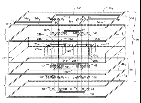
Referring now to FIG. 1, an electrical transformer 10 is shown having a core
12, here,
for example, a ferrite core, disposed between a pair of dielectrics 14, 16,
here, for example, a
pair of multilevel printed circuit boards 14, 16 as shown. The first
multilayer printed circuit
board 14 has a plurality of first electrically isolated electrical conductor
segments 14a-14f
disposed on each one of a plurality of electrically isolated levels, or
dielectric boards 14, and
142 of such first multilevel printed circuit board 14, Thus, electrically
isolated electrical
conductor segments 14a-14d are on different electrically isolated regions of
dielectric board
4
CA 02513384 2005-07-13
WO 2004/072997 PCT/US2004/002465
141 of board 14 and electrically isolated electrical conductor segments 14e
and 14f are on
different electrically isolated regions of dielectric board 142 of board 14.
The second multilayer printed circuit board 16 is disposed under, and is in
registration
with, the first multilevel printed circuit board 14. The second multilevel
printed circuit board
has a plurality of second electrically isolated electrical conductor segments
16a-16d disposed
on each one of a plurality of electrically isolated levels of such second
multilevel printed
circuit board 16. Thus, electrically isolated electrical conductor segments
16a and 16b are on
different electrically isolated regions of dielectric board 161 of board 16,
electrically isolated
electrical conductor segment 16c is on dielectric board 162 of board 16, and
electrical
conductor segment 16d is on dielectric board 163 of board 16. Each one of the
boards has
electrically conductive plated through holes, one portion of the plated
through holes being
indicated by the numerical designation 18 and the other portion being
indicated by the
designation S2-S9 and P2-P9.
It is noted that:
electrically conductive segment 14a has ends thereof connected between port PI
and
plated through hole P2;
electrically conductive segment 14b has ends thereof connected between plated
through hole S9 and port S 10;
electrically conductive segment 14c has ends thereof connected between plated
through hole S2 and port S1;
electrically conductive segment 14d has ends thereof connected between plated
through hole P9 and port P10;
electrically conductive segment 14e has ends thereof connected between plated
through hole S5 and plated through hole P5;
electrically conductive segment 14f has ends thereof connected between plated
through hole P6 and plated through hole P5;
electrically conductive segment 16a has ends thereof connected between plated
through hole P3 and plated through hole P4;
electrically conductive segment 16b has ends thereof connected between plated
through hole P7 and plated through hole P8;
electrically conductive segment 16c has ends thereof connected between plated
through hole S8 and plated through hole S7; and
5
CA 02513384 2005-07-13
WO 2004/072997 PCT/US2004/002465
electrically conductive segment 16d has ends thereof connected between plated
through hole S4 and plated through hole S3.
The core 12, shown more clearly in FIG. 2, has a plurality of apertures 20a,
20b
threrethough. When assembled, the apertures 20a, 20b extends between the first
and second
multilevel printed circuits boards 14, 16, as shown in FIG. 1. A pair of
dielectric bodies, here
for example, printed circuit boards 22a, 22b are disposed in the apertures
20a, 20b,
respectively as shown. Each one of the dielectric bodies 22a, 22b has disposed
therein a
plurality of electrically isolated electrical conductor segments, 24a through
24h, as shown.
Thus, here body 22a has electrical conductor segments 24a-24d thereon and body
22b has
electrical conductor segments 24e-24h, thereon, as shown.
The core 12 with the dielectric bodies 22a, 22b with the electrical conductor
segments
24a-24h are inserted into a dielectric spacer 30, as shown in FIGS. I and 3.
It is noted that the first and second multilevel printed circuit boards 14, 16
are
disposed in a pair of overlaying planes and the plurality of electrically
isolated electrical
conductor segments 24a-24h are disposed perpendicular to the overlaying
planes.
When assembled, first ends, here the upper ends in FIG. 1, of the electrically
isolated
electrical conductor segments 24a-24h are electrically connected to the
electrically isolated
electrical conductor segments 14a-14f and second ends, here the lower ends of
the
electrically isolated electrical conductor segments 24a-24h are electrically
connected to the
electrically isolated electrical conductor segments 16a-16h through the
electrically plated
through holes S2-S9 and P2-P9. More particularly, when assembled:
the upper ends of electrical conductor segments 24a-24h are electrically
connected to
plated through holes S9, P2, P6, S5, S6, P5, P9 and S2, respectively; and
the lower ends of electrical conductor segments 24a-24h are electrically
connected to
plated through holes S8, P3, P7, S4, S7, P4, P8 and S3, respectively
With such connections, a primary winding of the transformer 10 comprises port
P 1,
electrical conductor segments 14a, 24b, 16a, 24f, 14f, 24c, 16b, 24h, 14d and
port Pio and a
secondary winding comprises port S1, electrical conductor segments 14c, 24h,
16d, 24d, 14e,
24e, 16d, 24a, 14b and port S 10.
It is noted that the primary and secondary winding provide loops around the
portion
12a (FIG. 3) of the core 12. Further, it is noted that the electrically
isolated electrical
conductor segments 24a-24h are embedded within the core 12.
6
CA 02513384 2005-07-13
WO 2004/072997 PCT/US2004/002465
Referring now to FIG. 4, another embodiment is shown. Here, the transformer
10'
has the pair of multilevel printed circuit boards, 14 and 16, as described
above in connection
with FIGS. 1, 2 and 3. Here, however, adjacent portions of a pair of toroidal
shaped cores
12a, 12b provide the core. The pair of toroidal shaped cores 12a, 12b are
disposed within a
pair of apertures provided through the dielectric spacer 30', as shown. A pair
of circular
shaped dielectric bodies 22'a, 22'b having the electrically conductive
segments 24a-24b are
disposed within a corresponding one of the central, apertured, regions of the
toroidal shaped
bodies 12a, 12b as shown.
When assembled, first ends, here the upper ends in FIG. 4, of the electrically
isolated
electrical conductor segments 24a-24h are electrically connected to the
electrically isolated
electrical conductor segments 14a-14f and second ends, here the lower ends of
the
electrically isolated electrical conductor segments 24a-24h are electrically
connected to the
electrically isolated electrical conductor segments 16a-16h through the
electrically plated
through holes S2-S9 and P2-P9. More particularly, when assembled:
the upper ends of electrical conductor segments 24a-24h are electrically
connected to
plated through holes S9, P2, P6, S5, S6, P5, P9 and S2, respectively; and
the lower ends of electrical conductor segments 24a-24h are electrically
connected to
plated through holes S8, P3, P7, S4, S7, P4, P8 and S3, respectively
With such connections, a primary winding of the transformer 10 comprises port
P1,
electrical conductor segments 14a, 24b, 16a, 24f, 14f, 24c, 16b, 24g, l4d and
port P10 and a
secondary winding comprises port S 1, electrical conductor segments 14c, 24h,
16d, 24d, 14e,
24e, 16d, 24a, 14b and port S 10.
Thus, here the primary and secondary winding provide loops around the portion
12a
(FIG. 3) of the adjacent portions 12a' and 12b' of the cores I2a and 12b.
Further, it is noted
that the electrically isolated electrical conductor segments 24a-24h are
embedded within the
cores 12a and 12b, as shown. It is noted that segments 24b, 24c, 24f and 24g
provide the
vertical portions of the primary loop and segments 24h, 24d, 24e and 24a
provide the vertical
portions of the secondary loop.
It should be understood that the number of conductive segments through the
dielectric
bodies 22a, 22b or 22a', 22b' might be larger than the four segments shown
with the number
of conductive segments of the printed circuit boards being correspondingly
increased. Thus,
referring now to FIGS. 5 and 6, a modified exemplary one of the dielectric
bodies 22'a and
7
CA 02513384 2005-07-13
WO 2004/072997 PCT/US2004/002465
22'b, here body 22"a is shown. Here, the body 22"a has eight conductive
segments 24'S1-
24'S4 and24Pi-24P4. The conductive segments 24'S.1-24'S4 provide the vertical
portions of
the secondary loop and the conductive segments 24'P1-24'P4 provide the
vertical portions of
the primary loop. The eight conductive segments 24'S1-24'S4 and 24P1-24P4 have
upper and
lower conductive tabs 38 for making electrical connection to the plated
through holes of the
multilevel printed circuit boards 14, 16. Here, there is an electrically
conductive shield 40
disposed between the segments 24'S 1-24'S4 and the segments 24P1-24P4. The
electrically
conductive shield 40 has tabs 42 for connection to a ground plane, not shown,
of the
multilevel printed circuit boards, 14, and 16 and a vertical cutout that
prevents the shield
from introducing a shorted turn in the transformer. Here, the electrical
conductor segments
24'Si-24'S4 and 24P1-24P4 and the shield 40 are copper and are embedded within
an epoxy
filler 44.
As noted above, the body 22"a is disposed within the central region of the
toroidal
shaped core 12a.
Referring now to FIG. 7, an electrical transformer 10" is shown here with the
upper
multilayer printed circuit board 14 illustrated with only the electrical
conductive segments
used to interconnect transformer segments to be described in connection with
FIG. 8. Here,
the dielectric spacer member 30" has a plurality of, here 20, apertures
therethrough. The
apertures in the spacer member 30" pass between a top and a bottom surface of
the spacer
member. A plurality of toroidal shaped cores 12", as shown in FIG. 4 is
provided. Each one
of such cores 12" is disposed in a corresponding one of the plurality of
apertures of the
dielectric spacer member 30". Each one of the cores 12" has an aperture
therein, the
apertures of the cores 12" being coaxial with the apertures in the dielectric
spacer member
30". A plurality of dielectric bodies, here the body 22" as described above in
connection
with FIGS. 5 and 6 is provided. Each one of such dielectric bodies 22" is
disposed in a
corresponding one of the apertures in the cores 12".
Thus, a plurality of plurality of dielectric bodies 22" has a corresponding
one of the
vertical electrically isolated electrical conductor segments 24S1-24S4 and
24P1 - 24P4, as
described above in connection with FIGS. 5 and 6. The ends or tabs 38 of the
electrical
conductor segments are electrically connected to electrically isolated
electrical conductor
segments of the upper and lower multilevel printed circuits boards. Here,
however, the
boards 14, 16 are modified to provide not only primary and secondary windings,
or loops
8
CA 02513384 2012-05-22
78625-26
around each one of the toroidal shaped cores, i.e., to provide a transformer
segment 10', as
shown in FIG. 8, but the conductor segments on the multilevel printed circuit
boards are used
to electrically interconnect each one of the transformer segments 10' as shown
in FIG. 8, and
thereby provide a larger transformer assembly 10".
A number of embodiments of the invention have been described. Nevertheless, it
will
be understood that various modifications may be made without departing from
the
scope of the invention. Accordingly, other embodiments are within the scope of
the following
claims.
9