Note: Descriptions are shown in the official language in which they were submitted.
CA 02513415 2005-07-14
WO 2004/079351 PCT/US2004/006139
INTEGRATED TUNABLE OPTICAL SENSOR (ITOS) SYSTEM AND METHOD THEREFOR
Field of the Invention
The invention relates to optical sensors and spectroscopy systems, and more
particularly to optical sensors and spectroscopy systems which include ttmable
filters.
Background of the Invention
Although there has been active research and development regarding sensors,
there has
been very limited work on integrated systems that combine various featzzres
needed for
to certain practical sensor applications. Integrated senor systems are needed
in a wide variety of
applications including, medical diagnostics, homeland defense, forensic and
investigative,
pharmaceutical, food, and agricultural product analysis, environmental
bioremediation and
monitoring, bioprocess monitoring and biotechnology applications. Unlike
fundamental
research, portability of instmmentation is an important factor in
enviromnental field
15 monitoring and clinical applications.
Previously disclosed sensor systems have generally relied on commercially
available
spectrographs equipped with photomultipliers (PMTs) or 2-dimensional
detectors, such as
charge-coupled device (CCD) based systems, which require bulky electronic and
data
conditioning accessories. These detector systems required high-voltage power
supply systems
2o that often limit these systems for use under field conditions. Besides
being bulky, when used
in spectroscopy applications these devices limit the available spectroscopic
analysis
techniques which can be used. For example, phase-sensitive detection is not
possible using
conventional CCD based systems.
CA 02513415 2005-07-14
WO 2004/079351 PCT/US2004/006139
SUMMARY OF INVENTION
A scanning tunable detection system for analyzing a sample includes a source
of time
varying excitation signals, and a tunable optical filter for selectively
transmitting time-
varying optical signals emanated from the sample following irradiation with
the time varying
excitation signals. A detector is provided for converting the time-varying
optical signals to
electrical detection signals.
The tunable optical filter can comprise an AOTF or a LCTF. The system can
include
structure for modulating scanning of the AOTF. The system preferably includes
a data
treatment system for receiving the detection signals, the data treatment
system providing at
to least one of phase-sensitive and time-sensitive detection.
The system can include diffractive optics for dividing a beam from the source
of time
varying excitation signal into a plurality of discrete excitation light beams.
The discrete
excitation light beams can irradiate a plttraiity of locations on the sample.
The detector can
comprise a detector array including a plurality of pixels for receiving a
plurality of said time-
15 varying optical signals emanated from the respective locations on the
sample.
The detector can comprise at least one avalanche photodiode, or an array of
the same.
The system can also include structure for wirelessly transmitting the
detection signals.
The time-varying optical signals can comprise Raman signals or surface
enhanced-
Raman signals. The time-varying optical signals can comprise fluorescence
signals,
2o phosphorescence signals, or atomic emission signals.
The system can include a gated integrator for receiving the detection signals
or signals
derived (such as amplified, filtered, etc.) from the detection signals, the
gated integrator
integrating the detection signals only after a predetermined period of time
after the sample
irradiation has ceased. A train of pulses can be used to modulate the source
of excitation
CA 02513415 2005-07-14
WO 2004/079351 PCT/US2004/006139
signals, the train of pulses also applied to the gated integrator after the
predetermined period
of time.
The system can include a synchronous demodulator for receiving the time-
varying
electrical signals and a phase shift selector, wherein the phase shift
selector synchronizes the
synchronous demodulator to a modulation frequency applied to the excitation
source. In
another embodiment, the system ca.n include a synchronous demodulator for
receiving the
time-varying electrical signals and a phase shift selector, wherein the phase
shift selector
synchronizes the synchronous demodulator to a modulation frequency applied to
an output
of the excitation source.
l0 In yet another embodiment, the time-varying excitation signals can comprise
a pulse
train and the emanated signal can be a series of pulses, wherein the system
further comprises
a multiplexer for collecting the series of pulses and a first and second
counter synchronized
with the pulse train. The first counter can process "0" excitation states in
the detection
signals and the second counter can process "1" excitation states in the
detection signals. In
1 s this embodiment, a data collection and averaging module can be connected
to outputs of both
the first and the second counter.
A method for identifying at least one component in a sample includes the steps
of
providing a source of time-varying radiation, irradiating the sample with said
time-varying
radiation, wherein a time-varying optical signal emanates from the sample. The
time-varying
20 optical signals are then converted to electrical detection signals. The
electrical detection
signals are processed to provide time-varying measurements relating to the
sample. The
method can include the step of selectively transmitting time-varying optical
signals
emanating from the sample, such as using an AOTF or a LCTF. The optical
signals
comprises Raman signals, or other emanated signals including fluorescence
signals,
25 phosphorescence signals, or atomic emission signals.
CA 02513415 2005-07-14
WO 2004/079351 PCT/US2004/006139
The time-varying measurements can include lifetime determination or time
resolved
measurements. The time-varying measurements can include phase resolved
measurements.
The method can include the step of slew scanning. In slew scanning, the
scanned
range can be traversed in a non-constant fashion. Slew scanning permits
information rich
regions to more closely examined, while regions with little or no desired
information can be
quickly scanned over.
The method can include the step of delaying initiation of the converting step
for a
predetermined time after the irradiation. The time-varying source can provide
a modulated
frequency output, and the method further comprising the step of synchronizing
demodulation
io of said time-varying electrical signals with the modulated frequency. The
processing step can
comprise imaging the sample.
CA 02513415 2005-07-14
WO 2004/079351 PCT/US2004/006139
BRIEF DESCRIPTION OF THE DRAWINGS
A fuller understanding of the present invention and the features and benefits
thereof
will be accomplished upon review of the following detailed description
together with the
accompanying drawings, iri which:
FIG. 1 illustrates operational characteristics of a non-collinear AOTF, where
the
Bragg grating causes the wavelength of interest to be diffracted off from the
rest of the light
wavelengths at a slight angle.
to FIG. 2 illustrates a diagram of an integrated optical tunable sensor
system, according
to an embodiment of the invention.
FIG. 3A illustrates an exemplary excitation pulse and the resulting decay
curve
response provided by a sample.
FIG. 3B illustrates a train of periodic excitation pulses and the resulting
decay curve
responses.
FIG. 4 illustrates a modulated excitation pulse and the resulting modulated
emission
signal.
FIG. SA is a blocls diagram of a modulated excitation and synchronous
detection
system which utilizes analog demodulation.
5
CA 02513415 2005-07-14
WO 2004/079351 PCT/US2004/006139
FIG. SB is a block diagram of a modulated excitation and synchronous detection
system which utilizes analog demodulation and includes an electrooptic
modulator.
FIG. 5C is a block diagram of a pulsed excitation and gated detection system
utilizing
analog gated integration.
FIG. 6A is a block diagram of a modulated excitation and synchronous detection
system using digital demodulation.
FIG. 6B is a block diagram of a pulsed excitation and gated detection system
including a photon counting avalanche photodiode (APD) and digital techniques.
FIG. 6C is a block diagram of a modulated excitation and synchronous detection
system with wireless RF data transmission
FIG. 7 shows a Raman spectrum showing implementation of slew-scamling for an
ITOS system.
6
CA 02513415 2005-07-14
WO 2004/079351 PCT/US2004/006139
DETAILED DESCRIPTION OF THE PREFERRED EMBODIMENTS
The invention includes a sensor system comprising a dynamically tunable band
pass
optical filter which permits adjustment of transmission bands for selectively
passing time
varying optical signals emanated from an irradiated sample. A photodetector
converts the
time-varying optical signals into time-varying electrical signals.
A data treatment system is preferably provided for receiving the electrical
signals and
providing time-based measurements relating to the sample. The system is
referred to herein
as an Integr ated Tunable Optical Sensor (ITOS) system.
The invention provides significantly improved performance over earlier optical
sensor
to systems by combining several advanced detection and instrumental
approaches. Through
appropriate signal processing, detectors according to the invention can
provide time-resolved
measurements and/or phase-resolved measurements. The system can also provide
slew scan
measurements where the scanned range can be traversed in a non-constant
fashion. Slew
scanning permits information rich regions to more closely examined, while
regions with little
15 or no desired information can be quickly scanned over. Wireless data
transmission can be
used to transmit the sensor data to one or more remote locations.
The invention can be applied to various spectroscopic detection methods.
Although
the invention is generally described with respect to Raman spectroscopy, the
invention can be
practiced with other spectroscopic methods, such as absorption, emissions such
as
2o fluorescence and phosphorescence, and elastic scattering.
Raman spectroscopy, which is still an underexploited technique, can provide
some
significant advantages over other spectroscopic methods for field analysis.
Following laser
irradiation of a sample, the observed Raman shifts are equivalent to the
energy changes
involved in transitions of the scattering species and are therefore
characteristic of it. These
25 observed Raman shifts correspond to vibrational transitions of the
scattering molecule. Such
CA 02513415 2005-07-14
WO 2004/079351 PCT/US2004/006139
frequencies, when observed using absorption techniques, occur in the infrared
(IR) region of
the spectrum. Thus, in Ratnan spectroscopy, the spectrum of interest is in the
same spectral
region as the excitation radiation, such as laser radiation.
Raman spectroscopy provides more detailed vibrational information, which is
often
unavailable or unresolvable in fluorescence, UV absorption and reflectance
spectroscopy.
This information can be related to stuuctural changes in the molecules and to
the functions of
living tissues and cells. Raman spectroscopy is also more suitable than IR
spectroscopy for
biological analysis because it does not suffer from the strong IR absorption
band of water.
The laser wavelength can be selected in the near infrared (NIR) region far
away from the
1o water absorption band and where ambient light or room light do not
interfere with the
detection process. For these reasons, Raman spectroscopy has a great potential
for biomedical
diagnostics. In spite of these important features, there has been no disclosed
spectroscopy
system that provides the improved perfor-~nance needed for sensitive Raman
based detection.
The Raman effect is normally a weak process. Thus, low sensitivity
historically has
limited its applications. Recently, the Raman technique has been rejuvenated
following the
discovery of a Raman enhancement of up to about 10~ to 101° for
molecules adsorbed on
microstructures of metal surfaces. The technique associated with this
phenomenon is known
as surface-enhanced Raman scattering (SERS) spectroscopy. The enhancement is
due to a
microstructured metal surface scattering process which increases the
intrinsically weak
2o normal Raman scattering (NRS) due to a combination of several
electromagnetic and
chemical effects between the molecule adsorbed on the metal surface and the
metal surface
itself. In view of its sensitivity advantage over conventional Raman, the
invention is
generally preferably practiced using Raman spectroscopy by placing the sample
on a
nanostructured metal surface.
s
CA 02513415 2005-07-14
WO 2004/079351 PCT/US2004/006139
The enhancement is primarily due to plasmon excitation at the metal surface.
Thus,
the effect is generally limited to Cu, Ag and Au, and to a few other metals
for which surface
plasmons are excited by visible radiation. Although chemisorption is not
essential, when it
does occur there may be further enhancement of the Raman signal, since the
formation of
new chemical bonds and the consequent perturbation of adsorbate electronic
energy levels
can lead to a surface-induced resonance effect. The combination of surface-
and resonance-
enhancement, often referred to as surface-enhanced resonance Raman scattering
(SERRS)
can occur when adsorbates have intense electronic absorption bands in the same
spectral
region as the metal surface plasmon resonance, yielding an overall enhancement
as large as
to 101° to 1012
Nanoparticles can comprise solid metal of nanoscale size or nanoparticles
coated with
metal layers. Nanospheres of dielectric materials coated with a thin layer of
silver (metal
nanoshell) have been found to be SERS active. Nanospheres of magnetic
materials coated
with a thin layer of metal can also be used as SERS-active magnetic
nanoparticles. The core
diameter and the metal thickness of nanoshells can be varied to modify the
SERS properties
of the nanoparticles as disclosed in an article co-authored by the inventor.
[R. L. Moody, T.
Vo-Dinh, and W. H. Fletcher, "Investigation of Experimental Parameters for
Surface-
Enhanced Raman Spectroscopy," Appl. Spectrosc., 41, 966 (1987)].
The dynamically tunable optical band pass filter can be embodied as a tunable
optical
2o dispersion device, such as an Acousto-Optic Tunable Filter (AOTF). One of
the inventors has
disclosed a basic Raman monitoring using a system based on an AOTF [Ref: B.
Cullum, J.
Mobley, Z. Chi, D. L. Stolces, G. H. Miller, and T. Vo-Dinh, "Development of a
Compact,
Handheld Raman Instrument with No Moving Parts for use in Field Analysis,"
Rev. Sci.
Instrum., 71, 1602 (2000)]. An AOTF is a solid-state, electronically tunable
bandpass filter
which uses the acousto-optic interaction inside an anisotropic medium. The
filters can be
9
CA 02513415 2005-07-14
WO 2004/079351 PCT/US2004/006139
used with mufti-line sources (e.g mixed gas lasers, laser diodes) or with
broadband light
sources (e.g. xenon, halogen lamps). Tunable band pass filters allow the user
to adjustably
select and transmit a single wavelength from incoming light that includes a
plurality of
wavelengths.
The radio frequency (RF) applied to the AOTF transducer controls the
transmitted
(filtered in 1st order) wavelength. A complete spectrum analysis can be
acquired by varying
the RF frequency corresponding to the desired wavelength range. The RF
amplitude level
applied to the transducer controls the transmitted (filtered) light intensity
level. This is a
unique feature provided by the AOTF. The AOTF has a fast response time,
typically being
l0 several seconds, is accurate, and exhibits a high extinction ratio.
AOTFs offer several advantages over other available optical filters. An AOTF
is a
compact solid-state device, which has no moving mechanical parts, and an AOTF
can be
tuned to any wavelength within its operating range in microseconds. In
addition, AOTFs are
not limited by the small slit size associated with dispersive devices (e.g.
grating
15 monochromators). As a result, AOTFs can increase the light intensity
throughout the
detection using larger apertures. The relevant performance of AOTFs, such as
efficiency,
bandwidth, and rejection, are compared to that of typical small grating
monochromators.
AOTF technology offers the multiplex capability to monitor multiple sensors
simultaneously
at different locations or different samples. The system can also be used to
record entire
20 spectral images of samples. These characteristics, combined with the small
size of these
devices, make AOTFs an important new alternative to conventional
monochromators,
especially for portable instrumentation in field applications.
In AOTFs a piezoelectric transducer is bonded to a birefringent crystal
(typically
TeOz or quartz). The transducer is excited by a RF 50-200 MHz signal and
generates acoustic
25 waves in a birefringent crystal. Those waves temporarily establish a
periodic modulation of
to
CA 02513415 2005-07-14
WO 2004/079351 PCT/US2004/006139
the index of refraction via the elasto-optic effect. Under proper conditions,
the AOTF will
diffract part of the incident light within a narrow frequency range. This is
the basis of an
electronically tuned optical filter using the Bragg diffraction of light by
periodic modulations
in the index of refraction in the crystal established by the acoustic waves.
This "phase
grating" diffracts only light within a narrow frequency range. The Bragg
grating can diffract
only light that enters the crystal such that its angle to the normal of the
face of the crystal is
within a certain range. This range is referred to as the acceptance angle of
the AOTF.
Most AOTFs are based on a tellurium oxide (TeOz) crystal. Since it has high
acousto-
optical figure of merit, TeOz is the most common material used for AOTFs
operating in the
l0 visible and near-infrared. However, many compounds of interest exhibit
optimal absorption
and fluorescence emission peak values in the ultraviolet, and Te02 is not
transparent below
350nm. In contrast, a collinear-quartz AOTF will be used in this study. In
general, non-
collinear TeO2 AOTFs can have larger optical apertures than the collinear-
quartz type.
In a collinear AOTF the light incident at the optical window in the crystal is
linearly
15 polarized. Some of this polarized light is coupled to the diffracted light
beam. The
polarization of the diffracted (filtered) beam is orthogonal to the incident
light. Since the
diffracted beam and the incident light beam are collinear, a polarizer at the
exit of the crystal
separates them.
Figure 1 illustrates the operational characteristics of a typical non-
collinear AOTF,
2o where the Bragg grating causes the wavelength of interest (~,D) to be
diffracted off from the
rest of the light at a slight angle, such as about 6 degrees. The percentage
of light diffracted is
the diffraction efficiency of the device. This parameter greatly depends on
the incidence
angle, the wavelength selected and the power of the RF generator signal.
11
CA 02513415 2005-07-14
WO 2004/079351 PCT/US2004/006139
The AOTF spectral resolution, which is defined as the full width at half
maximum,0~,,
is given by:
~z
21~n sinz 9;
where ~, is the wavelength of observation, l is the interaction length between
the
acoustic wave and the light wave. Ofa = n~ - no; where n~ and no are index of
refraction of the
extraordinary and ordinary axis, respectively, in the anisotropic crystal;
while 8 is the
incident angle.
An alternative tunable sensor technology is based on liquid crystal tunable
filters
(LCTF). LCTFs are rapid switching, electronically tuned devices which employ
either a
to ferroelectric or a nematic liquid crystals (LC). The more commonly used
nematic LCTF
comprises a series of liquid crystal elements whose thiclcnesses are cascaded
in the same way
as the Lyot filter. However, the tuning is achieved by electronically rotating
the crystal axes
of the LC waveplate. When no voltage is applied, the retardance is at a
maximum. At large
applied voltages, the retardance reaches a minimum. The retardance can be
tuned
15 continuously to allow the wavelength to be tuned.
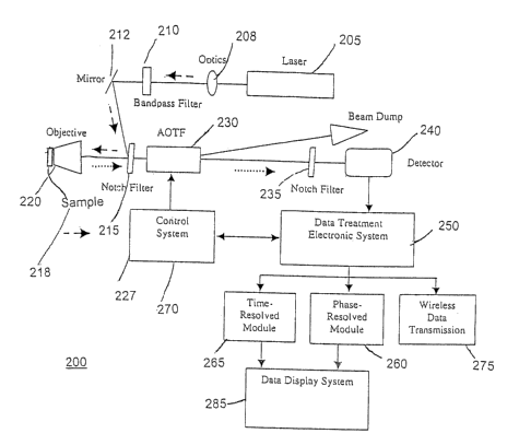
A schematic of an exemplary ITOS system 200 is shown in FIG. 2. System 200
includes an excitation source 205, such as a HeNe laser or a diode laser. For
example, a HeNe
laser (Melles Griot, OS-LHR-171, 7mW at 632.8 nm) or a diode laser (Process
Instuument)
can be used. Excitation light provided by excitation source 205 is diffracted
by optic/focusing
20 lens 208 which can provide a processed excitation light beam. Excitation
light passes through
bandpass filter 210 and is then reflected off of a reflecting mirror 212 onto
a holographic
notch filter 215, which again reflects the incident laser light. Notch filter
215 rejects (reflects)
a narrow frequency band centered at or near the laser frequency and transmits
signals in the
rest of the spectrum essentially unchanged.
12
CA 02513415 2005-07-14
WO 2004/079351 PCT/US2004/006139
Although optic/focusing lens 208 is shown providing a single processed
excitation
beam, optic/focusing lens 208 can provide a plurality of excitation light
beams. The
respective light beams can have an area to match the area of the respective
target areas on the
sample being tested to support optional imaging applications
The use of the mirror 212 is optional but is desirable to shorten the
dimension of the
system 200. The excitation light beam is adjusted at an incident angle
relative to a surface
normal of the notch filter 215 such that over the maximum amount (e.g. 98%) of
the incident
laser beam is reflected onto the objective. This reflected beam is directed
towards a
microscope objective 220, such as a 20ac microscope objective with a numerical
aperture of
l0 0.4 (Nikon, cat. # 85502), to be focused to a small area, preferably almost
to a point.
To measure a sample 218, the sample 218 is placed just in front of the
microscope
objective 220 and the backscattered light (e.g. Raman scatter) is then
collected and collimated
with the same objective 220. This design, which uses the same objective 220
for both
excitation as well as collection, allows maximum overlap of the excitation and
emission focal
15 volumes to be obtained. Once the scattered light is collimated by objective
220, it passes
through the first holographic notch filter 215 (e.g. Kaiser Optical Systems
Inc., notch plus-
633), which rejects the majority of the Raleigh scattered laser light while
allowing the Raman
shifted wavelength emanated from sample 218 to be transmitted. Both of the
holographic
notch filters (215 and 235) used in system 200 preferably provide an optical
density of
2o greater than 6.0 for the laser line and maximum transmission, approximately
74%, at 310 cm
1 and greater.
For most Raman measurements of organic compounds, 310 cni 1 is sufficiently
close
to the laser line for identification purposes and quantitative analysis.
However, holographic
notch filters with sharp notch edges, less than 150 cni ~, are commercially
available and can
25 be used with system 200. Light (e.g. Raman) that is transmitted through the
first holographic
13
CA 02513415 2005-07-14
WO 2004/079351 PCT/US2004/006139
notch filter 215 is then filtered by a tunable optical filter 230, such as an
AOTF (Brimrose,
TEAF-0.6-0.9-UH), for wavelength discrimination. The first order diffracted
light exiting the
AOTF 230 is then passed through a second holographic notch filter 235 to
further remove
any Rayleigh scattered light and to permit the Raman signal that has passed
through the
AOTF 230 and focused down onto a detector 240, such as a thermoelectrically
cooled
photon-counting avalanche photodiode (APD) (EG&G, SPCM-AQ-XY) with a f/1.3
lens.
Bandpass filter 230 can also be an LCTF or other equivalent scanning bandpass
filter
device. Using a detector 240 that provides 2-dimensional imaging capability,
bandpass filter
230 allows ITOS system 200 to provide mufti-spectral imaging (MSI) capability
or multiplex
to capability to monitor multiple sensors simultaneously at different
locations on a given sample
or a plurality of different samples. ITOS system 200 can also be used to
record the entire
spectral image of a sample.
Assuming bandpass filter 230 is an AOTF, by applying a RF signal to the
piezoelectric transducer an acoustic wave is propagated through the crystal.
This acoustic
15 wave spatially modulates the refractive index throughout the crystal, which
in turn causes
only light of a specific wavelength to be diffracted. W the AOTF 230 employed
in system
200, the crystal is cut and mounted so that the diffracted wavelength travels
along the same
path as the incident light while the zero order light is emitted at a six-
degree angle with
respect to the incident light. This device provides a spectral operating range
from 600 to 900
20 nm. With 632.8-nm excitation the Raman shift will correspond to a large
relative
wavenumber range (4691.7 cm 1)
The detector 240 is preferably an APD-based device. APD-based detectors
provide
several advantages over other detectors including small size, high quantum
efficiency over
the wavelength region of interest, and high amplification. Unlike CCDs, APDs
can be
25 manufactured using conventional integrated circuit processing, which
facilitates integration
14
CA 02513415 2005-07-14
WO 2004/079351 PCT/US2004/006139
of APDs with other electronic and optical components on chip. Photodiodes and
phototransistors can also be manufactured using conventional integrated
circuit processing
and can also be used with the invention.
An APD along with all its associated pulse generating electronics can be
contained in
a single box approximately 4.00 x 1.25 x 1.50 inches in size aiding in
producing a small final
instrument. In addition, APDs are among the most sensitive detectors for the
wavelength
range of interest. APDs have quantum efficiencies of approximately 70% and due
to the
inherent nature of APDs, thus reducing the possible added noise when an
external amplifier is
used. The photon counting APD described above provides a 2 V TTL pulse lasting
about 9
to ns for every photon detected.
For imaging applications, photodetector 240 can be a detector array comprising
a
plurality of independent detector pixels (not shown). In this embodiment, as
noted above,
optic/focusing lens 208 can provide a plurality of discrete excitation light
beams, the
respective light beams having an area to match the area of the respective
target areas on the
is sample being tested. Each of the respective target areas can be supported
by dedicated
detector pixels on the detector array. Data display system 285 can provide
imaged results
using data from the plurality of pixels.
The output of detector 240 is then sent to a data treatment electronic system
250. The
data treatment system 250 can comprise a universal counter where the
electronic pulses are
2o counted for a specific duration chosen in software. Alternatively, the
output of the detector
240 can be sent to various sub-systems comprising data treatment system 250
which can
provide various advanced detection modes, such as phase-sensitive detection
using phase
resolved module 260 or time-sensitive detection using time-resolved module
265. Data
display system 285 can display detection data provided by phase resolved
module 260 and/or
25 time-resolved module 265.
CA 02513415 2005-07-14
WO 2004/079351 PCT/US2004/006139
Control system 270 can also direct system 200 to operate in a slew scan mode.
In the
slew scan mode, band pass filter 230 is operated in a non-constant fashion.
For example,
band pass filter can be scanned slowly through spectral regions rich in
information but
quickly in regions without such information. Figure 7, which is discussed in
detail later,
describes such an embodiment.
Controller 270 can also allow system 200 to implement electronically modulated
scanning (EMS). In one embodiment, controller 270 includes an RF signal
generator (not
shown) for generating and applying a modulated RF signal to AOTF 230. The
modulated RF
signal modulates the scanning of the AOTF and produces a modulated light
output.
to Modulation of the AOTF scanning provides several advantages. Modulated
light output by
AOTF 230 can provide a phase-locked detection mode which can improve the
signal-to-
noise ratio. In addition, light can be modulated around a selected absorption
or emission
band of interest using this scanning mode.
A wireless data transmission module 275 can also be included with system 200.
15 Transmitter module 275 can include a mixer (not shown) for combining the
detection signal
with an RF carrier signal, an RF amplifier, transmitter, and antenna (not
shown) to permit
remote data treatment and analysis. The transmitter can be a transceiver to
permit reception
of control and other signals from one or more remote sources.
The ITOS system 200 can measure optical signals from a wide variety of
2o spectroscopic processes, including absorption, fluorescence,
phosphorescence, elastic
scattering, and Raman scattering. One important parameter of the signal
emanating from
samples of interest is the lifetime of the radiation emanated. The lifetimes
of selected various
processes are as follows:
(1) absorption: instantaneous with excitation
25 (2) fluorescence: 10-1° sec to 10-8 sec
16
CA 02513415 2005-07-14
WO 2004/079351 PCT/US2004/006139
(3) phosphorescence: 10-6 to 10-3 sec
(4) scattering: almost instantaneous with excitation
Two methods of measuring emanated signals that permit determination of
lifetimes
comprise time-resolved and phase-resolved methods. Time-resolved and phase-
resolved
methods can improve the signal-to-noise values by differencing the actual
signal of interest
from the background noise (DC signal).
In the time-resolved method, a pulsed excitation signal is used. The width of
the
excitation is generally much shorter than the emission or other process of
interest, so that the
excitation width is much shorter than the lifetime (decay time(s)) of the
samples. If it is
desired to measure the lifetime, the time-dependent emanated intensity I(t)
can be measured
following the excitation pulse. The decay time i can then be calculated from
the slope of a
plot of log T(t) versus t, or from the time at which the emanated signal
intensity (1) decreases
to 1/e (about 37%) of the initial emanated intensity value I(t=0).
To measure the emission (or other emanated signal) intensity free from
influence from
the excitation pulse, the detection process can begin after a delay time (dt)
sufficiently after
the excitation pulse such that the excitation pulse intensity has decreased
close to zero as
shown in FIG. 3A. Different compounds generally provide different
characteristic decay
time(s). Thus, compounds present in samples can be identified on the basis of
their decay
tunes.
For example, different compounds having different decay times can be
differentiated
by using different delay times (dT) and gate times (DT) as shown in FIG. 3B.
The gate time
(~T) corresponds to the portion of the decay curve in which detection takes
place For
example, the emission of a compound having a short decay time could be
detected using a
short gate time, while a longer decay time sample would require a longer gate
to properly
register (provide a good signal-to-noise value). To distinguish between these
two compounds
17
CA 02513415 2005-07-14
WO 2004/079351 PCT/US2004/006139
(with only one being present, but not knowing which one), one could perform
two
measurements using two different (short and long) gate times. If the
measurements using two
gate times show the same results (same signal intensities), it could be
concluded that the
compound with the short decay time is present, as all the short-decay emission
fits in the two
gate windows. However, if the two gate times produce different results (i.e.,
the signal
obtained with the short gate time is lower than the signal with the longer
gate time), it could
be concluded that the compound present was the one having a long gate time.
Similar
variations could be performed using a fixed gate time and varying the delay
time. A long
delay time would cause the measurement to miss short-decay emissions, but
register long-
1o decay emissions. A short delay time would register both emissions.
An important source of noise in many measurement situations is the DC noise
from
the background. Improvement in signal-to-noise can be achieved by using
multiple periodic
excitation pulses, and by applying the "boxcar" method by integrating the
emission signal
during a gate time (~T) after each pulse as also shown in FIG. 3B.
15 Another method that can be used to determine lifetimes involves phase-
resolved
techniques, which are often referred to as frequency domain techniques. In the
phase-resolved
technique, the sample is excited with intensity-modulated light. The intensity
of the incident
light changes with a very high frequency (w = 2~ f, f being the frequency in
hertz) as
compared to the reciprocal of the sample decay time i. Following excitation
with the high
2o frequency modulation signal, the emission or other signal emanation becomes
intensity-
modulated at the same modulation frequency. However, since the emission or
other
emanation from the sample follows a decay time, there is a certain delay in
the emission
relative to the excitation as shown in FIG. 4. This delay is generally
measured as a phase-shift
(o5), which can be used to calculate the decay time. At each modulation
frequency ~r, the
is
CA 02513415 2005-07-14
WO 2004/079351 PCT/US2004/006139
delay is described as the phase shift Via, which increases from 0° to
90° with increasing
modulation frequency ~.
The finite time response of sample also results in demodulation of the
emission by a
factor ma. This factor decreases from 1.0 to 0 with increasing modulation
frequency. At low
frequency, the emission or other signal emanated closely follows the
excitation signal.
Accordingly, the phase angle is near zero and the modulation is near 1. As the
modulation
frequency is increased, the finite lifetime of the emission or other emanation
process prevents
the emission from closely following the excitation. Tlus results in a phase
delay of the
emission, and a decrease in the peals-to-peak amplitude of the modulated
emission or other
1 o signal emanated.
The shape of the frequency response is determined by the number of decay times
displayed by the sample. If the decay is a single exponential, the frequency
analysis is
simplified. in this case, the phase angle or modulation at any frequency can
be used to
calculate the lifetime. For single-exponential decay, the phase and modulation
are related to
15 the decay time (i) by the following relations:
tan ~a = ~s i ; and m~, _ (1 + ~z .~z) -nz
Therefore, one can differentiate and thus identify various emissions or other
signal
emanations having different decay times by selecting the phase shift (~)
optimized to the
decay time (i) of interest. This method is generally refeiTed to phase-
resolved detection.
2o Figure SA illustrates an ITOS system 500 which includes a modulated
excitation
source and synchronous detection using analog intensity modulation. A crystal
oscillator 505
provides a modulation frequency to a frequency selector 510 (e.g. programmable
timer)
which is driven by a frequency control 512, which selects the frequency used
to run laser
driver module 520, which drives laser 525. The laser driver 520 modulates the
intensity of the
25 laser light emitted by laser 525, which is used to excite the target sample
52~. The laser 525
19
CA 02513415 2005-07-14
WO 2004/079351 PCT/US2004/006139
can be modulated, such as 50% on-time and 50% off time. The Raman signal (or
other signal
emanated, such as fluorescence, phosphorescence) is band pass filtered by a
band pass filter,
such as AOTF 530, which is driven by RF driver 532.
AOTF 530 isolates the emission or other signal of interest from other
interferences,
such as laser scattered light and background noise. Assuming Raman detection
is desired, the
isolated Raman signal is detected by detector 535, such as an avalanche
photodiode (ADP) or
a photomultiplier (PMT), or an array of the same, which converts the emanated
signal (e.g.
Raman signal) into an electrical signal.
Output current provided by detector 535 (e.g. APD) is amplified using an
amplifier
l0 538 having sufficient bandwidth to pass the excitation frequency, since the
excitation signal
is also used as the phase input to the synchronous demodulator 540. The
synchronous
demodulator 540 is operated by a phase-shift selector 541, which is
synchronized with the
laser excitation modulation frequency. This arrangement synchronously
rectifies the output
provided by amplifier 538. A low-pass filter 542 is used to average the output
of the
15 synchronous demodulator 540. To the first order, any signal not having the
same frequency
as the excitation frequency is averaged to zero, so this approach rejects do
and other
interference signals. The output of low pass filter 542 is then provided to
analog-to-digital
converter (ADC) 545, which provides a digital data output 550.
The finite time response of the sample also results in demodulation of the
emission or
20 other emanated signal by a factor m.~. As noted earlier, for single-
exponential decay, the
phase and modulation are related to the decay time (i) by tan ~.~ _ 'err i and
m°, _ (1 + ~z ,~z) -
vz. Therefore, for Raman, fluorescence and phosphorescence detection, various
emissions or
other emanated signals having different decay times can be differentiated by
selecting a phase
shift (~) optimized to the decay time (i) of interest (phase-resolved
detection). The phase-
25 resolved technique is also helpful for distinguishing the modulated signal
emanated from the
CA 02513415 2005-07-14
WO 2004/079351 PCT/US2004/006139
sample (e.g. Raman signal) from the do background signal, such as signals from
sun light or
room light.
Figure 5B shows an ITOS system 560, which closely parallels system 500 shown
in
FIG. 5A. System 560 is also adapted for phase-resolved detection. Rather than
directly
modulating laser 525 in system 500, system 560 modulates the output of laser
525 by
applying a modulating signal, such as to electro-optic modulator 565 (e.g.
Pockels cell) or
other light modulator to modulate the laser excitation light. System 560 can
provide
advantages over system 500 in certain system arrangements. For example, some
lasers may
not be physically be able to be modulated as shown in system 500, or if they
are, their
to frequency or amplitude stability may be compromised.
Figure 5C shows an ITOS system 570 with pulsed excitation and gated detection
using analog gated integration. An oscillator (such as a crystal oscillator)
505 provides the
modulation frequency to a frequency selector 510 (e.g. programmable timer),
which selects
the frequency used to run laser driver module 520 using inputs from pulse rate
and pulse
15 width control 513. The laser driver module 520 triggers pulses from laser
525 used to excite
the target sample 528. The resulting Raman (fluorescence, or other) signal
emanated from the
sample is detected via a tunable optical filter, such as AOTF 530, which is
used to isolate the
Raman or other emanated signal from other interferences (e.g., laser
scattering, baclcground
noise). The isolated emanated signal is detected by detector 535 (e.g., APD),
which converts
2o the optical signal into an electrical signal. The electrical signal is
amplified by the amplifier
540 and then fed to gated integrator 572.
The gated integrator 572 opens "the detection gate" to process detection
signal data
only when it receives a signal from a gate generator 573, which is triggered
by a delay
generator 574. The delay generator is preferably driven by the same excitation
pulses output
25 by frequency selector 510 that triggers laser driver 520, but set a time
delay (dt) between the
21
CA 02513415 2005-07-14
WO 2004/079351 PCT/US2004/006139
excitation pulses and the opening of the detection gate as shown earlier in
FIG. 3B.
Therefore, it is possible to eliminate influence from laser scatter by setting
a sufficient time
delay (dt) delay period.
Alternatively it is possible to decrease the fluorescence background from the
Raman
or other signal of interest. For example, fluorescence emission from the
background which
generally has different decay times i can also be discriminated from the Raman
signal of
interest by using different time delay (dt) values optimized to the target
probe decay times.
The signal from the gated integrator 572 is then fed into a bandpass filter
576 and then
preferably to a power averaging circuit (not shown). Finally the analog signal
is fed into an
to analog-to-digital converter (ADC) 545, which provides a digital data output
550 which
represents the detection signal.
Figure 6A shows an ITOS system 600 with modulated excitation and synchronous
detection using digital demodulation. An oscillator (such as a crystal
oscillator) 605 provides
a base frequency to a frequency selector 610 (e.g. programmable timer), which
generates the
15 modulation frequency used to run laser driver module 620. The laser driver
620 modulates
the intensity light from laser 625 which is used to excite the target sample
628. The Raman
signal (or, e.g. fluorescence, phosphorescence) is detected via an AOTF or
similar band pass
filter 630, which is used to isolate the emission or other detection signal
from other
interferences (e.g., laser scattering, background noise). The isolated Raman
(fluorescence)
20 emission is detected by the detector 635 such as an avalanche photodiode
(ADP) or a
photomultiplier (PMT), which converts the luminescence signal into an
electrical signal. The
detector should include electronic circuits to produce pulses from the
detected Rarnan
(luminescence) signal. Alternatively, the electrical signal from the detector
can be amplified
by an optional amplifier, and then passed to a comparator or discriminator to
produce pulses
25 (both not shown in FIG. 6A).
22
CA 02513415 2005-07-14
WO 2004/079351 PCT/US2004/006139
The laser light is modulated, such as using a 50% duty cycle pulse provided by
laser
driver 620. Accordingly, the signal emanated from the sample which is detected
by detector
635 (e.g. APD) is in digital form (a series of logic pulses with nearly a 50%
duty cycle). The
pulses are collected in a multiplexer 638, and then fed to two counters. For
example, counter
639 can provide processing for "0" excitation states and counter 640 for
processing "1"
excitation states. The onloff cycles of the two counters 639 and 640 are
synchronized with the
excitation/detection cycle by enabling each with the same modulated excitation
waveform
provided by laser driver 620 which drives laser 625. For example, counter 639
can be
enabled when the laser excitation cycle is off, and thus can provide the
baclcground signal.
to The other counter 640 is enabled when the laser excitation cycle is on, and
thus provides the
signal emanated from sample 628. The delay time of the counter cycle can be
varied in order
to perfornl phase-resolved measurements. The digital signals from both
counters 639 and 640
can be fed into a data collection and averaging module 642, where the
detection signal can be
processed (e.g., background subtraction, etc) before being output as digital
data out 644 .
15 Figure 6B shows an ITOS system 650 with pulsed excitation and gated
detection
using digital gated integration. System is similar to system 600 and uses the
elements of
system 600 to perform the function of system 570. Unlike system 600, the
excitation is not a
square wave, rather it is a sequence of pulses. Like system 570, this system
provides gated
integration. This is accomplished by gating on (enabling) the appropriate
counter to receive
20 pulses produced during excitation on or off times. Figure 6B shows the same
signal input to
the laser driver 620 and the counter enable 640, but gate and delay generators
(like 574 and
573 shown in Fig. 5C) could be added in between programmable timer 610 and
counters 639
and 640.
Figure 6C shows a Wireless ITOS system 670 with modulated excitation,
25 synchronous detection and RF data transmission. System 670 is analogous to
system 500
23
CA 02513415 2005-07-14
WO 2004/079351 PCT/US2004/006139
shown in FIG. 5A, except ADC 545 in system 500 is replaced by mixer 680 and RF
amplifier
685. Thus, in system 670, the detection signal is not digitized by the system,
but is rather
transmitted wirelessly using a radio-frequency (RF) linlc.
The RF carrier frequency can be the same as used the laser excitation for
system 670
as shown in FIG. 6C. The detected signal coming output by synchronous
demodulator 540 is
then filtered by low-pass filter 542 to provide a low fiequency (near dc)
detection signal,
which is used to modulate the RF carrier via mixer 680 as shown in FIG. 6C.
The resulting
modulated earner signal is then amplified by the RF amplifier 685 and
transmitted. A
remotely located receiver (not shown) can demodulate the transmitted signal
and extract the
to low-frequency Raman or other signal of interest for digitization and other
data processing.
One advantage of ITOS technology is the ability to operate in the "slew
scanning"
mode. Slew scanning mode can vastly improve signal-to-noise values of
measurements by
concentrating on discrete and generally narrow spectral regions of interest.
Figure 7 shows
the principle of slew scan mode applied to Raman spectroscopy. For example, a
Raman
15 spectrum of a compound usually covers wave numbers between about 2000 to
3000 cm 1.
However, generally only 2-5 peaks are sufficient to unambiguously identify the
compound
being interrogated. These Raman pealcs are usually very narrow (less than 1
cni 1) and depend
on the spectral resolution of the instruments (5-10 cm 1 for the Brimrose
AOTFs used in
Raman measurements). Therefore, if it is necessary to identify a specific
compound in a
2o complex mixture, it is only generally necessary to scan only a few (e.g. 2-
3) narrow spectral
regions where the Raman peaks are known to be located. The slew scan method
can be
applied to other emission spectra which generally exhibit a limited number of
narrow
emission peaks, such as atomic emission, atomic absorption, and atomic
fluorescence.
Figure 7(a) shows an exemplary Raman spectnim which includes a plurality of
peaks.
25 Assume that Raman peaks in each of the wave number ranges Ova, Ovb, and Ovc
can
24
CA 02513415 2005-07-14
WO 2004/079351 PCT/US2004/006139
unambiguously identify a particular target. Ova, wb, and Ovc are shown in FIG.
7(b)
including respective peaks shown in FIG. 7(a). In contrast to the slew scan
mode, in a
conventional scan mode the entire spectral range from vo to vF is scanned at a
constant rate.
A scanning tunable bandpass filter, such as a AOTF or LCTF can be programmed
to
slowly scan Ova, wb, and Ovc regions (for example 10 cm 1 each, or a total of
only 30 cm 1),
which are rich in spectral information of interest. The scanning tunable
bandpass filter can
rapidly scan over other regions outside these narrow regions in the full range
from vo to vF.
This method is referred to as the "slew scanning" mode and is unique to the
present
invention.
to The slew scanning mode camlot be performed with multichannel detectors such
as
charge-coupled devices (CCDs) where the entire spectral regions must be
collected. Thus,
CCD based systems primarily produce mea~iingless data outside the spectral
regions) of
interest. For example, to record an entire Raman spectrum using CCD devices,
data must
generally be recorded for the full 3000 cm 1.
15 On the other hand, the slew scan method of the ITOS needs to only record
data of 30
cm ~, i.e. 100 times less data to record. Therefore the ITOS can be operated
approximately
100 times faster then CCDs and obtain the most meaningful important
information (e.g., data
for 3 typical peaks). Alternatively, for the same measuring time, the ITOS can
spend more
time at the spectral region of interest (about 100 longer measuring time) in
order to improve
20 signal-to-noise values.
In an alternate embodiment, the ITOS can have a broader use. The slew scan
scheme
can be viewed as a "dynamic multi-element match filter" (DMMF) for a point-
source or for a
2-dimensional image using multiple point sources. A DMMF comprises software
that can be
programmed and integrated into the system such that the device can search for
a specific
2s
CA 02513415 2005-07-14
WO 2004/079351 PCT/US2004/006139
compound by scanning over a preselected combination of peaks characteristic of
the
compounds of interest.
Systems according to the invention can be fully integrated and light enough
and small
enough to be readily portable, thus being suitable for field use. Such systems
can provide
direct identification and quantitative analysis of chemical and biological
samples in a few
seconds under field conditions. An exemplary AOTF-based system according to
the
invention including diode laser and APD detector that was built measured 22 x
5 x 4 inches
and weighed approximately 35 pounds. A waterproof housing enclosed the system
making
the system waterproof and complying with NEMA-4 standards. The water proof
feature
to permits systems according to the invention to undergo decontamination
procedures without
special preparation, an important requirement for a system used in hazardous
environments.
Power sufficient for about 3 hours of system operation was provided by a
common
lithium ion battery. Longer operation times with an increase in system size or
weight can be
provided by higher energy density batteries. The system included a single
board computer
15 which controls operation of the system as well as data analysis and
storage. The computer
included several general purpose digital input/output ports which interfaced
to the various
electronics including a touchscreen display. Power for the system was provided
by a lithium
ion battery.
Systems according to the invention can thus be used in a wide variety of
applications.
2o For example, homeland defense, forensic and investigative, medical
diagnostics,
pharmaceutical, food, and agricultural product analysis, environmental
bioremediation and
monitoring, bioprocess monitoring and biotechnology applications.
While the preferred embodiments of the invention have been illustrated and
described,
it will be clear that the invention is not so limited. Numerous modifications,
changes,
26
CA 02513415 2005-07-14
WO 2004/079351 PCT/US2004/006139
variations, substitutions and equivalents will occur to those skilled in the
art without
departing from the spirit and scope of the present invention as described in
the claims.
27