Note: Descriptions are shown in the official language in which they were submitted.
CA 02513574 2005-07-18
WO 2004/066346 PCT/CA2004/000076
1
DOPED SEMICONDUCTOR NANOCRYSTAL LAYERS, DOPED SEMICONDUCTOR
POWDERS AND PHOTONIC DEVTCES EMPLOYING SUCH LAYERS OR POWDERS
FIELD OF THE INVENTION
The present invention relates to semiconductor
nanocrystal layers and powders doped with rare earth elements,
to semiconductor structures comprising these semiconductor
nanocrystal layers, to processes for preparing the
semiconductor nanocrystal layers doped with rare earth
elements, and to photonic devices employing these materials~
BACKGROUND OF THE INVENTION
Silicon has been a dominant semiconductor material in
the electronics industry, but it does have a disadvantage in
that it has poor optical activity due to an indirect band gap.
This poor optical activity has all but excluded silicon from
the field of optoelectronics. In the past two decades there
have been highly motivated attempts to develop a silicon-based
light source that would allow one to have combined an
integrated digital information processing and an optical
communications capability into a single silicon-based
integrated structure. For a silicon-based light source
(silicon Light Emitting Diode (LED)) to be of any practical
use, it should (1) emit at a technologically important
wavelength, (2) achieve its functionality under practical
conditions (e. g. temperature and pump power), and (3) offer
competitive advantage over existing technologies.
One material that has gathered much international
attention is erbium (Er) doped silicon (Si). The light
emission from Er-doped Si occurs at the technological important
1.5 micr~n (lZm) wavelength. Trivalent erbium in a proper host
can have a fluorescence of 1540 nm due to the 4113/2-> 4115/2
intra-4f transition. This 1540 nm fluorescence occurs at the
minimum absorption window of the silica-base telecommunication
CA 02513574 2005-07-18
WO 2004/066346 PCT/CA2004/000076
2
fiber optics field. There is great interest in Er doping of
silicon as it holds the promise of silicon based
optoelectronics from the marriage of the vast infrastructure
and proven information processing capability of silicon
integrated circuits with the optoelectronics industry.
Theoretical and experimental results also suggest that Er in Si
is Auger-excited via carriers, generated either electrically or
optically, that are trapped at the Er-related defect sites and
then recombine, and that this process can be very efficient due
to strong carrier-Er interactions. However, if this strong
carrier-Er interaction is attempted in Er-doped bulk Si, the
efficiency of the Er3+ luminescence is reduced at practical
temperature and pump powers.
Recently, it has been demonstrated that using
silicon-rich silicon oxide (SRS~), which consists of Si
nanocrystals embedded in a Si~2 (glass) matrix, reduces many of
the problems associated with bulk Si and can have efficient
room temperature Er3+ luminescence. The Si nanocrystals act as
classical sensitizer atoms that absorb incident photons and
then transfer the energy to the Er3+ ion, which then fluoresce
at the 1.5 micron wavelength with the following significant
differences. First, the absorption cross section of the Si
nanocrystals is larger than that of the Er3+ ions by more than 3
orders of magnitude. Second, as excitation occurs via Auger-
type interaction between carriers in the Si nanocrystals and
Er~ø ions, incident photons need not be in resonance with one of
the narrow absorption bands of Er3+. However, e~~isting
s.pproaches to developing such Si nanocrystals have only been
successful at producing concentrations of up t~ 0.3 atomic
percent of the rare earth element, which is not sufficient for
practical applications. A schematic of the energy mechanisms
of erbium doped silicon-rich silicone oxide is shown in Figure
13.
CA 02513574 2005-07-18
WO 2004/066346 PCT/CA2004/000076
3
In general, manufacture of type IV semiconductor
nanocrystals doped with a rare earth element is done by ion
implantation of silicon ions into a silicon oxide layer,
followed by high temperature annealing to grow the silicon
nanocrystals and to reduce the ion implantation damage. The
implantation of Si ions is followed by an ion implantation of
the rare earth ions into the annealed silicon nanocrystal oxide
layer. The resulting layer is again annealed to reduce the ion
implant damage and to optically activate the rare-earth ion.
There are several problems with this method: i) it
results in a decreased layer surface uniformity due to the ion
implantation; ii) it requires an expensive ion implantation
step; iii) it fails to achieve a uniform distribution of group
IV semiconductor nanocrystals and rare-earth ions unless many
implantation steps are carried out; and iv) it requires a
balance between reducing the ion implant damage by thermal
annealing while trying to maximise the optically active rare-
earth.
To diminish the above drawbacks, Plasma Enhanced
Chemical Vapor Deposition (PECVD) has been utilised to make
type IV semiconductor nanocrystal layers. The prepared layers
are then subjected to a rare-earth iori implantation step and a
subsequent annealing cycle to form the IV semiconductor
na~nocrystals, and to optically activate the rare-earth ions
that are ~.oped in the nanocrystal region. 'Unfortunately, the
layers prepare. with this methodl are still subjected to an
implantation step, whioh results in a decrease in surface
uniformity.
Another PECVD method that has been used to obtain a
doped type IV semiconductor crystal layer consists of co-
sputtering together both the group IV semiconductor and rare-
earth metal. In this method, the group IV semiconductor and a
rare-earth metal are placed into a vacuum chamber and exposed
CA 02513574 2005-07-18
WO 2004/066346 PCT/CA2004/000076
4
to an Argon ion beam. The argon ion beam sputters off the
group IV semiconductor and the rare-earth metal, both of which
are deposited onto a silicon wafer. The film formed on the
silicon wafer is then annealed to grow the nanocrystals and to
optically activate the rare-earth ions. As the rare earth
metal is in solid form, the argon ion beam (plasma) is only
able to slowly erode the rare earth, which leads to a low
concentration of rare earth metal in the deposited film. While
higher plasma intensity could be used to more quickly erode the
rare earth metal and increase the rare earth concentration in
the film, a higher intensity plasma damages the film or the
group IV semiconductor before it is deposited. The plasma
intensity is therefore kept low to preserve the integrity of
the film, therefore limiting the rare earth concentration in
the film. The doped group Iv semiconductor nanocrystal layers
made through this method have the drawbacks that: i) the layer
does not have a very uniform distribution of nanocrystals and
rare-earth ions, ii) the layer suffers from upconversion
efficiency losses due to rare-earth clustering in the film, and
iii) the concentration of rare earth metal in the layer is
limited by the plasma intensity, which is kept low to avoid
damaging the layer.
The concentration of the rare earth element in
semiconductor nanocrystal layers is preferably as high as
possible, as the level of photoelectronic qualities of the
film, such as photoluminescence, is proportional to the
concentration. ~ne problem encountered when a high
concentration of rare earth element is present within the
semiconductor layer is that when two rare earth metals come
into close proximity with one another, a quenching relaxation
interaction occurs that reduces the level of photoelectronic
dopant response observed. The concentration of rare earth
element within a semiconductor film is thus balanced to be as
CA 02513574 2005-07-18
WO 2004/066346 PCT/CA2004/000076
high as possible to offer the most fluorescence, but low enough
to limit the quenching interactions.
In the past history of the semiconductor development
silicon has been considered unsuitable for the optoelectronic
5 applications. This is from the indirect nature of its energy
band gap, bulk silicon is indeed a highly inefficient light
emitter. There have been different approaches developed to
overcome this problem, quantum confinement in silicon
nanostructures and rare earth doping of crystalline silicon
have received a great deal of attention. Of particular
interest is silicon nanoclusters (NC) embedded in SiO2 in recent
years attracted interest of the scientific community as a
promising new material for the construction of visible Si-based
Light Emitting Diodes (LED).
The telecommunications industry commonly uses ~ptical
fibers to transmit large amounts of data in a short time. One
common light source for optical-fiber communications systems is
a laser formed using erbium-doped glass. One such system uses
erbium-doped glass fibers to form a laser that emits at a
wavelength of about 1.536 micrometer and is pumped by an
infrared source operating at a wavelength of about 0.98
micrometer. One method usable for forming wave guides in a
~w'17.~2strate 7.~w desCr7.bed 7.n LT.S. Pat . N~. 5, 080, 5Q3 Issued
Jan. 19:, 199 to lfajafi et al., which is hereby incorporated
~5 by reference. ~. phosphate glass useful in lasers is described
in LT.S. Pat. i~To. 5, 334, 559 issued ~.ug. 2, 199 to Joseph S.
Hayden, which is also hereb~r incorporated by reference. ~n
integrated optic laser is described in U'.S. Pat. l~To.
5,491,708 issued Feb. 13, 1996 to Malone et al., which is also
hereby incorporated by reference.
There is a need in the art for an integrated optical
system, including one or more high-powered lasers along with
routing and other components that can be inexpensively mass-
CA 02513574 2005-07-18
WO 2004/066346 PCT/CA2004/000076
6
produced. The system should be highly reproducible, accurate,
and stable.
In the area of opto-electronic packages, it is
generally accepted that the most time consuming and costly
component of the package is the alignment of the optical fiber,
or wave guide, to the semiconductor emitter or receiver. The
traditional approach to this alignment requires that the two
parts be micromanipulated relative to each other while one is
operating and the other is monitoring coupled light. ~nce the
desired amount of coupled light is attained, the two parts must
be affixed in place in such a way as to maintain this alignment
for the life of the product. This process, commonly referred
to as active alignment, can be slow and given to poor yields
stemming from the micromanipulation and the need to permanently
affix the two objects without causing any relative movement of
the two with respect to each other.
To alleviate this problem, opto-electronic package
designs have been suggested which incorporate passive alignment
techniques. These designs do not require activation of the
opto-electronic device. Generally, they rely on some
mechanical features on the laser. and the fiber as well as some
intermediate piece for alignment. By putting the pieces
together with some adhesion mechanism, alignment can be secured
and maintained for the life of the component. Typical of this
technology is the silicon optical bench ~.esign. In this
design, the laser is aligned via solder or registration marks
to an intermediate piece, a silicon part, which has mechanical
features--"v-grooves" --which facilitate alignment of an
optical fiber. The drawbacl~s to this design are the number of
alignments in the assembly process and the cost of the
intermediate component. Additionally, these designs can be
difficult to use with surface emitting/receiving devices
CA 02513574 2005-07-18
WO 2004/066346 PCT/CA2004/000076
7
because of the need to redirect the light coupled through the
system.
Other approaches have been suggested which do not
incorporate a silicon intermediate structure. Swirhun et al.
(U.S. Pat. No. 5,631,988) suggests that defined features in
a surface emitting laser array could be used as an alignment
means for a structure that holds embedded optical fibers. This
third structure adds complexity and adds to the overall
tolerance scheme for the alignment system.
In other prior art, attempts have been made to cope
with the dilemma of adding intermediate parts and their
associated costs and tolerances. I~tatsuda (U.S. Pat. No.
5,43,939) suggests a design that allows direct fiber coupling
to a laser by way of a guiding hole feature in the backside of
the actual laser substrate. The precision with which such
guiding holes can be manufactured is not currently adequate for
reliable coupling. Additionally, the process of making a hole
in the actual laser substrate can weaken an already fragile
material. Furthermore, this design is not appropriate when it
is desired to have light emit from the top surface of the opto-
electronic device, commonly called a top emitter in the
vernacular of the industry. In contrast, a bottom emitter is a
photonic device wherein the emitted light propagates through
the substrate and out the bottom surface of the device.
~dhat is needed is a photonic de~rice that allows
direct passive alignment and attachment of an optical signal
carrying apparatus, such as an optical fiber for example, via.
robust guide features formed integrally on the surface of the
photonic device. This photonic device would enable precise
positioning of the fiber relative to the active region with the
potential for sub-micron alignment accuracy without the
addition of interfacial alignment components. Furthermore, it
CA 02513574 2005-07-18
WO 2004/066346 PCT/CA2004/000076
8
would be advantageous if the fabrication method for the above
is compatible with standard semiconductor processing equipment.
Optical combiner devices are generally known. Such
devices may be used to receive multiple pump signals via
respective input ports and to combine the pump signals into an
pump source. The input signals may have different operational
wavelengths. The combined signal may be used to energize an
optical amplifier, for example.
It has been suggested to locate fiber gratings
upstream from the input ports of the combiner device to control
and/or stabilize the wavelengths of the respective optical
sources. One problem with this approach, however, is that it
can be difficult to match the wavelength characteristics of the
fiber gratings to the acceptance bandpass characteristics of
the input ports. The spectral misalignment can be caused by
normal manufacturing variations, by temperature variations, and
by other factors. Any misalignment between the spectral
characteristics of the gratings and the input ports of the
combiner device can result in a loss of optical efficiency.
This also has the caveat that the pump sources are coherent
i.e. lasers.
In general, a fiber type light amplifier including an
optical fiber having a core doped with a rare earth element
s~xch e.s erbium (Er) or the like is used as a light amplifier
used in an optical communication system.
In a typical arrangement of a fiber type light
amplifier, a signal light with a wave-length of 1.53 (gym passing
through an optical fiber is input to a wave synthesizer. The
wave synthesizer synthesizes a pumping light with a wavelength
of 1.48 ,um supplied from a pumping light output unit and the
signal light and supplies the same to an Er-doped optical
fiber. The Er-doped optical fiber absorbs the pumping light
CA 02513574 2005-07-18
WO 2004/066346 PCT/CA2004/000076
9
and amplifies the signal light. A wave separator separates the
amplified signal light from the pumping light which has not
been absorbed by the Er-doped light fiber and outputs only the
signal light to an optical fiber.
Nevertheless, this fiber type light amplifier has a
drawback in that the attachment of the wave synthesizer and
wave separator to the Er-doped optical fiber and the adjustment
thereof is time consuming. Further, the miniaturization of the
amplifier as a whole is difficult because a lower limit exists
in the winding radius of the long Er-doped optical fiber and an
extra length is needed to the portion of the Er doped optical
fiber to be connected to the wave synthesizer and wave
separator.
To overcome the above drawback, there is recently
proposed a planar type optical amplifier including an
amplifying core, a core having a function as a wave
synthesizer, and a core having a function as a wave separator
formed thereto, these cores being made by etching a glass film
obtained by doping with a type IV semiconductor nanocrystal
with a rare earth element such as erbium (Er) or the like on a
silicon substrate or quartz glass substrate.
SUMMARY ~F THE INVENTION
According to one broad aspect, the invention provides
a doped semiconductor powder comprising nanocrystals of a gr~~p
~5 IV semiconductor and a rare earth element, the rare earth
element being dispersed on the surface of the group IV
semiconduct~r nanocrystals.
According to another broad aspect, the invention
provides a photonic device comprising at least one integral
formed from a REDGIVN (rare earth doped group iv nanocrystal)
material.
CA 02513574 2005-07-18
WO 2004/066346 PCT/CA2004/000076
According to another broad aspect, the invention
provides a photonic device comprising: an amplification medium
comprising REDGINV; a plurality of light sources; a combiner
adapted to combine light from the plurality of light sources to
5 produce a broadband optical pump source which pumps light into
the amplification medium.
According to another broad aspect, the invention
provides a method of manufacturing a planar type optical
amplifier comprising: forming a bar-shaped core on a plane
substrate; forming a groove to the core which extends to the
longitudinal direction thereof; filling the groove with a
filler containing REDGI~f; and solidifying the filler.
According to another broad aspect, the invention
provides a method of preparing a photonic device with an
15 integral guide formed from a type Iv semiconductor nanocrystal
doped with rare earth ion material.
According to another broad aspect, the invention
provides a method of preparing a REDGIVN wave guide on a
photonic device comprising the steps of applying a resist,
20 transferring an image to the resist, and developing the image.
According to another broad aspect, the invention
provides a method of preparing a plated REDGI'~ guide on a
photonic device comprising the steps of s.pplying a resist,
transferring an image to the resist, developing the ims.ge,
plating the resist, and removing the resist.
According to another broad aspect, the invention
provides a photonic device comprising an LED comprising REDGI~
(rare earth doped group I~T nanocrystal) material.
According to another broad aspect, the invention
provides a photonic device comprising an optical laser
comprising REDGIVi~TT material.
CA 02513574 2005-07-18
WO 2004/066346 PCT/CA2004/000076
11
According to another broad aspect, the invention
provides a photonic device comprising a laser component
comprising: a thin film containing REDGIVN and having a
plurality of wave guides defined by channels within the
substrate; one or more feedback elements for providing optical
feedback to the wave guides to form a respective laser-
resonator cavity in each wave guide with a distinct resonance
characteristic to provide lasing action at a selected
wavelength when pumped, wherein injection of pump light at one
or more suitable wavelengths into the laser-resonator cavity
causes output of laser light at the selected wavelength in
accordance with a longitudinal cavity mode of the cavity.
The above and other objects, features and advantages
of the present invention will become apparent from the
following description when taken in conjunction with the
accompanying figures which illustrate preferred embodiments of
the present invention by way of example.
BRIEF DESCRIPTION OF THE FIGURES
Embodiments of the invention will be discussed with
reference to the following Figures:
Figure l is a diagram of a semiconductor structure
comprising a substrate, a doped semiconductor nanocrystal
layer, and a current injection layer;
Figure 2 is a diagram of ~. superlattice semiconductor
structure comprising a substrate and alternating doped
semiconductor ns.nocry~stal layers aid dielectric layers;
Figure 3 is a diagram of a Pulse Laser Deposition
apparatus;
Figure 4 displays a schematic of a gas pyrolysis
apparatus suitable for the production of a group Iv
semiconductor powder doped with a rare earth element;
CA 02513574 2005-07-18
WO 2004/066346 PCT/CA2004/000076
12
Figure 5 is a schematic diagram of a first LED which
uses Group IV semiconductor nanocrystals doped with rare-earth
ions, provided by an embodiment of the invention;
Figure 6 is a schematic diagram of another LED
provided by an embodiment of the invention, adapted to produce
white light;
Figure 7 is a schematic of an array of LEDs provided
by an embodiment of the invention;
Figure 8 is a schematic diagram of a Fabry-Perot
Cavity laser provided by an embodiment of the invention;
Figure 9 is a schematic diagram of a distributed
feedback laser provided. by an embodiment of the invention;
Figure 10 is a schematic diagram of an array of DFB
lasers provided by an embodiment of the invention
Figure 11 is a schematic diagram of an array of v-
grooved lasers;
Figure 12 is a schematic diagram of an electrically
pumped SRS~ laser provide by another embodiment of the
invention;
Figure 13 is a schematic of energy mechanisms of
erbium doped SRS~;
Figure 1~ is a perspective view of a~. e~am~al.e planar
optical circuit provided by an embodiment of the invention;
Figure 15 is a side view of a broadband optical pump
provided by an embodiment of the invention;
Figure Z6 is a cross section of the broadband optical
pump of Figure 15; and
CA 02513574 2005-07-18
WO 2004/066346 PCT/CA2004/000076
13
Figure 17 is a side view of a planar optical
amplifier provided by an embodiment of the invention.
DETAILED DESCRIPTION OF THE PREFERRED EMBODIMENTS
Doped Semiconductor Nanocrystal Layer
The doped semiconductor nanocrystal layer of the
invention comprises a group IV oxide layer in which is
distributed semiconductor nanocrystals. The group IV element
used to prepare the layer is preferably selected from silicon,
germanium, tin and lead, and the group IV semiconductor oxide
layer is more preferably silicon dioxide. The group IV oxide
layer preferably has a thic~~ness of from 1 to 2000 nm, for
example of from 30 to 2000 nm, from 100 to 250 nm, from 30 to
50 nm, or from 1 to l0 nm.
The semiconductor nanocrystals that are dispersed
within the group IV semiconductor oxide layer are preferably
the nanocrystal of a group IV semiconductor, e.g. Si or Ge, of
a group II-VI semiconductor, e.g. ZnO, ZnS, ZnSe, CaS, Care or
Case, or of a group III-V semiconductor, e.g. GaN, GaP or GaAs.
The nanocrystals are preferably from 1 to 10 nm in size, more
preferably from 1 to 3 rim in size,land most preferably from 1
to 2 nm in size. Preferably, the nanocrystals are present
within the group IV semiconductor oxide layer in a
concentration of from 30 to 50 s.tomic percent, more preferably
in a concentration of 37 to ~.°7 atomic percent, and most
preferably in a concentration of from 9:0 to ~~5 atomic percent.
The one or more rare earth element that is dispersed
on the surface of the semiconductor nanocrystal can be selected
to be a lanthanide element, such as cerium, praseodymium,
neodymium, promethium, gadolinium, erbium, thulium, ytterbium,
samarium, dysprosium, terbium, europium, holmium, or lutetium,
or it can be selected to be an actinide element, such as
thorium. Preferably, the rare earth element is selected from
CA 02513574 2005-07-18
WO 2004/066346 PCT/CA2004/000076
14
erbium, thulium, and europium. The rare earth element can, for
example, take the form of an oxide or of a halogenide. Of the
halogenides, rare earth fluorides are preferred as they display
more intense fluorescence due to field distortions in the rare
earth-fluoride matrix caused by the high electronegativity of
fluorine atoms. Most preferably, the rare earth element is
selected from erbium oxide, erbium fluoride, thulium oxide,
thulium fluoride, europium oxide and europium fluoride.
The one or more rare earth element is preferably
present in the group IV semiconductor oxide layer in a
concentration of 0.5 to 15 atomic percent, more preferably in a
concentration of 'S to Z5 atomic percent and most preferably in.
a concentration of 10 to 15 atomic percent. While such a high
concentration of rare earth element has led to important levels
of quenching reactions in previous doped semiconductor
materials, the doped semiconductor nanocrystal layer of the
present invention can accommodate this high concentration as
the rare earth element is dispersed on the surface of the
semiconductor nanocrystal, which nanocrystal offers a large
surface area. The reduced amount of quenching reactions
between the rare earth element and the proximity of the rare
earth element to the semiconductor nanocrystal provide the
basis for a doped semiconductor nanocrystal layer that offers
improved optoelectronic properties.
~5 5'~itl~.~~32~1~ot~~' I~a~'ei St~'i~ot~ie
Using the doped semiconductor nanocrystal layer
described above, a multitude of semiconductor structures can be
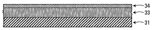
prepared. For example, a semiconductor structure is shown in
Figure 1, in which. one or more layers 33 of the doped
semiconductor nanocrystal layer are deposited on a substrate
31.
CA 02513574 2005-07-18
WO 2004/066346 PCT/CA2004/000076
The substrate on which the semiconductor nanocrystal
layer is formed is selected so that it is capable of
withstanding temperatures of up to 1000°C. Examples of
suitable substrates include silicon wafers or poly silicon
5 layers, either of which can be n-doped or p-doped (for example
with 1x10²° to 5x10²¹ of dopants per cm3) , fused silica, zinc
oxide layers, quartz and sapphire substrates. Some of the
above substrates can optionally have a thermally grown oxide
layer, which oxide layer can be of up to about 2000nm in
10 thickness, a thickness of 1 to 20 nm being preferred. The
thickness of the substrate is not critical, as long as thermal
and mechanical stability is retained.
The semiconductor structure can comprise a single or
multiple doped semiconductor nanocrystal layers, each layer
15 having an independently selected composition and thick~.ess. By
using layers having different rare earth elements, a multi-
color emitting structure can be prepared. For example,
combining erbium, thulium and europium in a single
semiconductor structure provides a structure that can fluoresce
at the colors green (erbium), blue (thulium), and red
(europium).
When two or more doped semiconductor nanocrystal
layers are used in a single semiconductor structure, the layers
can optionally be separated by a dielectric layer. Examples of
~5 suitable dielectric layers include silicon dioxide, silicon
nitrite and silicon oxy nitrite. The silicon dio~~i~.e
dielectric ls.yer can also optionally comprise semiconductor
nanocrystals. The dielectric layer preferably has a thickness
of from 1 to 10 nm, more preferably of 1 to 3 nm and. most
preferably of about 1.5 nm. The dielectric layer provides an
efficient tunnelling barrier, which is important for obtaining
high luminosity from the semiconductor structure.
CA 02513574 2005-07-18
WO 2004/066346 PCT/CA2004/000076
16
The semiconductor structure can also have an Indium
Tin Oxide (ITO) current injection layer (34) overtop the one or
more doped semiconductor nanocrystal layers. The ITO layer
preferably has a thickness of from 150 to 300 nm. Preferably,
the chemical composition and the thickness of the IT0 layer is
such that the semiconductor structure has a conductance of from
30 to 70 ohms cm.
The thickness of the semiconductor structure is
preferably 2000 nm or less, and the thickness will depend on
the thickness of the substrate, the number and thickness of the
doped semiconductor nanocrystal layers present, the number and
the thickness of the optional dielectric layers, and the
thicl~ness of the optional IT0 layer.
One type of preferred semiconductor structure
provided by an embodiment of the present invention is a
superlattice structure, shown by way of example in Figure 2,
which structure comprises multiple layers of hetero-material 60
on a substrate 51. Multiple doped semiconductor nanocrystals
layers having a thickness of from 1 nm to 10 nm are deposited
on the substrate 52 and 54, and the doped semiconductor
nanocrystals layers can comprise the same or~different rare
earth elements. Optionally, the doped semiconductor
nanocrystal layers are separated by dielectric layers 53 of
s.bout 1.5 nm in thickness, and s.n IT0 current injection layer
(not shown) can be deposited on top of the multiple layers of
the superlattice structure. There is no ma~~imum thickness for
the superlattice structure, ~.lthough a thickness of from X50 to
2000 nm is preferred and s. thickness of from X50 to 750 nm is
more preferred.
Prelaarati~n of the .I~~ped Se.mic~nduc~tor .111'~.nocrystal L~.~rer
The preparation of the doped semiconductor
nanocrystal layer comprises the following two general steps:
CA 02513574 2005-07-18
WO 2004/066346 PCT/CA2004/000076
17
(a) the simultaneous deposition of a semiconductor
rich group IV oxide layer and of one or more rare earth
element; and
(b) the annealing of the semiconductor rich group TV
oxide layer prepared in (a) to form semiconductor nanocrystals.
The semiconductor rich group IV oxide layer comprises
a group IV oxide layer, which group IV oxide is preferably
selected from SiO~ or GeO~, in which group IV oxide layer is
dispersed a rare earth element and a semiconductor, which
semiconductor can be the same as, or different than, the
semiconductor that forms the group IV oxide layer.
By "semiconductor rich", it is meant that an excess
of semiconductor is present, which excess will coalesce to form
nanocrystals when the semiconductor rich group IV oxide layer
is annealed. Since the rare earth element is dispersed within
the oxide layer when the nanocrystals are formed, the rare
earth element becomes dispersed on the surface of the
semiconductor nanocrystals upon nanocrystal formation.
Since the semiconductor rich group IV oxide layer arid
the one or more rare earth element are deposited
simultaneously, ion implantation of the rare earth element is
avoided. ~.s such, the group IV oxide layer surface is free of
the dame.ge associate. with an implantation process. also,
since the rare earth element is deposited at the same time as
~5 the semiconductor rich group IV oxie~e layer, the distribution
of the rare earth element is substantie.lly constant through the
thic~~ness of the group IV oxide layer.
The deposition of the semiconductor rich group IV
oxide layer doped with one or more rare earth elements is
preferably carried out by Plasma-Enhanced Chemical Vapor
Deposition (PECVD) or by Pulse Laser Deposition (PLD). The
above two methods each have their respective advantages for
CA 02513574 2005-07-18
WO 2004/066346 PCT/CA2004/000076
18
preparing the semiconductor rich group IV oxide layer doped
with one or more rare earth elements, and the methods are
described below.
Pulse Laser Deposition
Pulse laser deposition is advantageous for the
deposition of the semiconductor rich group IV oxide layer doped
with one or more rare earth elements as it permits the
deposition of a wide variety of semiconductors and a wide
variety of rare earth elements.
Referring now to Figure 3, which shows by way of a
diagram a typical set up of a pulse laser deposition apparatus,
the pulse laser deposition apparatus consists of a large
chamber 41, which can be evacuated down to at least 10-' bars or
pressurised with up to 1 atmosphere of a gas such as oxygen,
nitrogen, helium, argon, hydrogen or combinations thereof. The
chamber has at least one optical port 42 in which a pulse laser
beam 45 can be injected to the chamber and focused down onto a
suitable target 44. The target is usually placed on a carrousel
43 that allows the placement of different target samples into
the path of the pulse laser focus beam. The carrousel is
controlled so that multiple layers of material can be deposited
day the pulse laser ablation of the tare~et. The flue of the
focused ~aulse laser beam is adjusted so that the target ablates
approximatel~~ 0.1 nm of thickness of material on a substrs.te
47, which can be held perpendicular to the target and s.t a
distance of 20 to 75 millimetres above the target. This flux
for instance is in the range of 0.1 to 20 joules per square cm
for 248 nm KrF excimer laser and has a pulse width of 20 - 45
nanosecond duration. The target can be placed on a scanning
platform so that each laser pulse hits a new area on the
CA 02513574 2005-07-18
WO 2004/066346 PCT/CA2004/000076
19
target, thus giving a fresh surface for the ablation process.
This helps prevent the generation of large particles, which
could be ejected in the ablation plume 46 and deposited on to
the substrate. The substrate is usually held on a substrate
holder 48, which can be heated from room temperature up to
1000°C and rotated. from 0.1 to 30 RPM depending on the pulse
rate of the pulse laser, which in most cases is pulsed between
1-10 Hz. This rotation of the substrate provides a method of
generating a uniform film during the deposition process. The
laser is pulsed until the desired film thickness is met, which
can either be monitored in real time with an optical thicltness
monitor or quartz crystal microbalance or determined from a
calibration run in which the thickness is measured from a given
flux and number of pulses. Pulse laser deposition can be used
for depositing layers of from 1 to 2000nm in thickness.
For the preparation of a semiconductor rich group IV
oxide layer doped with one or more rare earth elements, the
target that is ablated is composed of mixture ~f a powdered
group IV binding agent, a powdered semiconductor that will form
the nanocrystal, and a powdered rare earth element. The ratio
of the various components found in the doped semiconductor
nanocrystal layer is decided at this stage by controlling the
ratio of the components that form the target. Preferably, the
mixture is placed in a hydraulic press and pressed into a. disk
of ~5mm diameter and 5mm thickness with a press pressure of at
les.st 500 Psi while: being heated to 700°~. The temperature and
pressure can be applied, for example, for one hour under
reduced. pressure (e. g. 10-~ bars) for about one hour. The press
pressure is then reduced and. the resulting target is allowed to
cool to room temperature.
The group I'~T binding agent can be selected to be a
group IV' oxide (e. g. silicon oxide, germanium oxide, tin oxide
or lead oxide), or alternatively, it can be selected to be a
CA 02513574 2005-07-18
WO 2004/066346 PCT/CA2004/000076
group IV element (e. g. silicon, germanium, tin or lead). When
the group IV binding agent is a group IV oxide, the binding
agent, the semiconductor and the rare earth element are
combined to form the target, and the pulse laser deposition is
5 carried out in the presence of any one of the gases listed
above. If a group IV element is used as the group TV binding
agent instead, the pulse laser deposition is carried out under
an oxygen atmosphere, preferably at a pressure of from 1x10⁻⁴ to
5x10⁻³ bar, to transform some or all of the group IV element
10 into a group TV oxide during the laser deposition process.
When the semiconductor element which is to form the
nanocrystals is selected to be a group II-VI semiconductor
(e.g. ~n~, ~nS, ~n5e, Cad, CaTe or Cafe) or a group III-V
semiconductor (e. g. Gate, ~aP or GaA.s), the oxygen concentration
15 is kept high to insure that all of the group IV element is
fully oxidized. Alternatively, if the nanocrystals to be
formed comprise the same group IV semiconductor element that is
being used as the binding agent, the oxygen pressure is
selected so that only part of the group IV element is oxidized.
20 The remaining non-oxidized group IV element can then coalesce
to form nanocrystals when the prepared semiconductor rich group
IV oxide layer is annealed.
The powdered rare earth element that is used to form
the t~.rget is preferably in the form of a rare earth oxide or
of a rare earth halogenide. ~s mentioned above, the rare earth
fluoride is the most preferred of the rs.:~e earth halogenides.
Pulse l~.ser deposition is useful for the subsequent
deposition of two or more different layers. ~°iultiple targets
can be placed on the carrousel and the pulse laser can be
focussed on different targets during the deposition. Using
this technique, layers comprising different rare earth elements
can be deposited one on top of the other to prepare
semiconductor structures as described earlier. Different
CA 02513574 2005-07-18
WO 2004/066346 PCT/CA2004/000076
21
targets can also be used to deposit a dielectric layer between
the semiconductor rich group IV oxide layers, or to deposit a
current injection layer on top of the deposited layers. Pulse
laser deposition is the preferred method for preparing the
superlattice semiconductor structure described above.
Preparation of the semiconductor rich group IV oxide
layer doped with one or more rare earth elements can of course
be carried out with different pulse laser deposition systems
that are known in the art, the above apparatus and process
descriptions being provided by way of example.
Plasma E.nhanc~ed Chemical Va~aor Deposition
PEC''7D is advantageous for the deposition of the
semiconductor rich group IV oxide layer doped with one or more
rare earth element, as it permits the rapid deposition of the
layer. The thickness of the semiconductor rich group IV oxide
layer doped with one or more rare earth element prepared with
PECVD is 10 nm or greater, more preferably from 10 to 2000 nm.
Formation of a non-doped type IV semiconductor
nanocrystal layer through chemical vapor deposition has been
described, for example, by J. Sin, M. Kim, S. Seo, and C. Lee
[Applied Physics Letters, (1990 , Volume 72, 9, 1092-1094), the
disclosure of which is hereby incorporated by reference.
In this embodiment, the doped semiconductor
n~.n~c:~ystal layer is prepared by incorporating a rare-earth
precursor into the PECVD stream above the receiving heated
substrate on which the semiconductor film is grown. PECVD can
be used to prepare the doped semiconductor nanocrystal layer
where the semiconductor nanocrystal is a silicon or a germanium
nanocrystal, and where the rare earth element is a rare earth
oxide.
CA 02513574 2005-07-18
WO 2004/066346 PCT/CA2004/000076
22
In the PECVD process, a group IV element precursor is
mixed with oxygen to obtain a gaseous mixture where there is an
atomic excess of the group IV element. An atomic excess is
achieved when the ratio of oxygen to group IV element is such
that when a group IV dioxide compound is formed, there remains
an excess amount of the group IV element. The gaseous mixture
is introduced within the plasma stream of the PEVCD instrument,
and the silicon and the oxygen are deposited on a substrate as
a group IV dioxide layer in which a group IV atomic excess is
found. It is this excess amount of the group IV element that
coalesces during the annealing step to form the group IV
nanocrystal. For example, to prepare a silicon dioxide layer
in which silicon nanocrystals is dispersed, a silicon rich
silicon oxide (SF.S~) layer is deposited on the substrate.
The group IV element precursor can contain, for
example, silicon, germanium, tin or lead, of which silicon and
germanium are preferred. The precursor itself is preferably a
hydride of the above elements. A particularly preferred group
IV element precursor is silane (SiH4).
The ratio (Q) of group IV element precursor to oxygen.
can be selected to be from 3:1 to 1:2. If an excess of group
IV element precursor hydride is used, the deposited layer can
contain hydrogen, for example up to approximately 10 atomic
percent hydrogen. The ratio of the flow rates of the group IV
element precursor and of o~~ygen can be ~~ept, for example,
between 2:1 and 1:2.
Also introduced to the plasma stream is a rare earth
element precursor, which precursor is also in the gaseous
phase. The rare earth precursor is added t~ the plasma stream
at the same time as the group IV element precursor, such that
the rare earth element and the group IV element are deposited
onto the substrate simultaneously. Introduction of the rare
earth precursor as a gaseous mixture provides better dispersion
CA 02513574 2005-07-18
WO 2004/066346 PCT/CA2004/000076
23
of the rare earth element within the group Iv layer.
Preferably, presence of oxygen in the plasma stream and in the
deposited layer leads to the deposition of the rare earth
element in the form of a rare earth oxide.
The rare earth element precursor comprises one or
more ligands. The ligand can be neutral, monovalent, divalent
or trivalent. Preferably, the ligand is selected so that when
it is coordinated with the rare earth element, it provides a
compound that is volatile, i.e. that enters the gaseous phase
at a fairly low temperature, and without changing the Chemical
nature of the Compound. The ligand also preferably Comprises
organic components that, upon exposure to the plasma in the
PECVD apparatus, will form gaseous by-products that can be
removed through gas flow or by reducing the pressure within the
PEC'VD apparatus. Then the organic Components of the ligand are
Conducive to producing volatile by-products (e. g. C~Z, ~~) less
organic molecules are incorporated into the deposited layer.
Introduction of organic molecules int~ the deposited layer is
generally not beneficial, and the presence of organic molecules
is sometimes referred to as semiconductor poisoning.
Suitable ligands for the rare earth element Can
include acetate functions, for example 2,2,6,6-tetramethyl-3,5-
heptanedione, acetylacetonate, flurolacetonate, 6,6,7,7,~,8,8-
heptafluoro-2,2-dimethyl-3,5-octanedione, i-
propylcyclopentadienyl, cyClopentadienyl, and n-
bta.t~~lCyclopentadien~~l. Preferred. rare earth metal prec~.rsor
inClu~.e t-ris(~,2,f,6-tetramethyl-3,5-heptanedionato)
erbium(III), erbium (III) acetylacetonate hydrate, erbium (III)
flurolacetonate, tris(6,6,7,7,~,8,~-heptafluoro-2,2-dimethyl-
3,5-octanedionate)erbium (III), tris(i-
propylcyclopentadienyl)erbium (III),
Tris(cyclopentadienyl)erbium (III), and tris(n-
butylcyclopentadienyl)erbium (III). A particularly preferred
CA 02513574 2005-07-18
WO 2004/066346 PCT/CA2004/000076
24
rare earth element precursor is tris(2,2,6,6-tetramethyl-3,5-
heptanedionato ) erbium ( I I I ) ( Er+3 [ ( CH3 ) 3CCOCH=COC ( CH3 ) s l s )
, which
is also referred to as Er+3(THMD)3.
If the rare earth element precursor is not in the
gaseous phase at room temperature, it must be transferred to
the gaseous phase, for example, by heating in an oven kept
between 80°C and 110°C. The gaseous rare earth element
precursor is then transferred to the plasma stream with an
inert carrier gas, such as argon. The gaseous rare earth
element precursor is preferably introduced to the plasma at a
position that is below a position where the group IV element
containing compound is introduced to the plasma. 'Use can be
made of a dispersion mechanism, for example a dispersion ring,
to assist in the dispersion of the gaseous rare earth element
precursor in the plasma.
In order to obtain a more even deposition of the
doped type IV oxide layer, the substrate can be placed on a
sceptre that rotates during deposition. A circular rotation of
about 3rpm is suitable for increasing the uniformity of the
layer being deposited.
An Electron Cyclotron Resonated (ECR) reactor is
suitable for producing the plasma used in the PECVD method
described above. ECR is a particular method of generating
plasma, where the electrons have a spiral motion caused by a
magnetic field, which allows a high density of ions in ~? low-
pressure region. The high ion density with low pressure is
beneficial for deposition, as the rare earth metal precursor
can be stripped of its organic components and incorporated
uniformly and in a high concentration.. The plasma used in the
PECVD method can comprise, for example, argon, helium, neon or
xenon, of which argon is preferred.
CA 02513574 2005-07-18
WO 2004/066346 PCT/CA2004/000076
The PECVD method is carried out under a reduced
pressure, for example 1x10-' torr, and the deposition
temperature, microwave power and scepter bias can be kept
constant. Suitable temperature, microwave and scepter bias
5 values can be selected to be, for example, 300°C, 400W and
-200VD~, respectively.
The semiconductor rich group IV oxide layer doped
with one or more rare earth element can be grown at different
rates, depending on the parameters used. A suitable growth
10 rate can be selected to be about 60 nm per minute, and the
semiconductor rich group IV oxide layer can have a thickness of
from 10 to 2000 nm, more preferably of from 100 to 250 nm.
Preparation of the semiconductor rich group IV oxide
layer doped with one or more rare earth elements can of course
15 be carried out with different plasma enhanced chemical vapor
deposition systems that are known in the art, the above
apparatus and process descriptions being provided by way of
example.
Annealing Step
20 After the semiconductor rich group IV oxide layer
doped with one or more rare earth element has been prepared,
the doped type IV oxide layer is annealed, optionally under
flowing nitrogen (i~TZ) , in a ~a~aid. Thermal Anneal (ETA.) furnace,
at from about 600°C to about 1000°C, more preferably from
300°C
25 to X50°C, from 5 minutes to 30 minutes, more preferably from 5
to ~ minutes. It is e~uring the annealing step that the atomic
excess of semiconductor is converted into semiconductor
nanocrystals.
When PECVD is used to prepare the semiconductor rich
group IV oxide layer doped with one or more rare earth element,
the annealing step can also be carried out under an oxygen
CA 02513574 2005-07-18
WO 2004/066346 PCT/CA2004/000076
26
atmosphere to insure oxidation of the rare earth element, or
under a reduced pressure in order to facilitate the removal of
any volatile by-products that might be produced.
The amount of excess semiconductor in the group IV
oxide layer and the anneal temperature dictate the size and the
density of the semiconductor nanocrystal present in the final
doped semiconductor nanocrystal layer.
Since the rare earth element is well dispersed
through the deposited group IV semiconductor oxide layer, when
the nanocrystals are formed during the annealing step, the rare
earth element becomes localised on the surface of the
nanocrystals. Since the nanocrystals provide a large surface
area on which the rare earth. element can be dispersed, the
concentration of the rare earth element can be quite elevated,
while retaining good photoelectronic properties.
Doped Semiconductor Por~der
The present invention also teaches the simple
manufacturing of a doped semiconductor powder, which
semiconductor powder comprises nanocrystals of a group IV
semiconductor and a rare earth element.
The doped semiconductor powder comprises as a major
component nanocrystals of a group IV semiconductor. The group
IV semiconductor can be selected, e.g., from silicon,
germanium, tin or lead, of which silicon and germanium are
preferred. combinations of these semicon~.uctors can also be
used, as well as mufti-element semiconductors that comprise the
above semiconductors. Preferably, the nanocrystals have an
average diameter of from 0.5 to 10 nm, for example of about 3
nm.
The rare earth element that is dispersed on the
surface of the semiconductor nanocrystals is preferably
CA 02513574 2005-07-18
WO 2004/066346 PCT/CA2004/000076
27
selected from cerium, praseodymium, neodymium, promethium,
gadolinium, erbium, thulium, ytterbium, samarium, dysprosium,
terbium, europium, holmium, lutetium, and thorium, of which
erbium, thulium and europium are most preferred. The rare
earth element is preferably in. the form of a complex comprising
a rare earth and one or more ligands. The nature of the one or
more ligands is dictated by the process used to prepare the
doped semiconductor powder. The doped semiconductor powders of
the invention can also comprise more than a single rare earth
element.
Since the rare earth element is dispersed on the
surface of the group T~7 semiconductor nanocrystal, reduced
photoactivity due to aggregation of the rare earth element is
reduced. The concentration of the rare earth element in the
doped semiconductor powder is preferably from 0.5 to 10 atomic
percent, more preferably from 0.5 to 5 atomic percent, and most
preferably from 0.5 to 2 atomic percent. The atomic percent
values are calculated on the basis of the number of rare earth
atoms relative the total number of atoms in the doped
semiconductor powder.
Gas P~rrol~rsis
A gas pyrolysis process can be utilised to prepare
the doped semiconductor powder of the invention. In this
process, a. group I~ semiconductor precursor and a rare earth
element complex are mixed in the gaseous phase, anc~ the mixture
is first heated, ~.nd then cooled to obtain the desired prod~.ct.
The gas pyrolysis reaction consists of the thermal treatment of
a gaseous group I'~ element, in the presence of a gaseous rare
earth element, to such a temperature that the gaseous group I'~7
element forms a nanocrystal. When the formed nanocrystal is
cooled down in the presence of a rare earth element, the rare
earth element goes form the gaseous state to the solid state
and it deposits itself on the surface of the nanocrystal.
CA 02513574 2005-07-18
WO 2004/066346 PCT/CA2004/000076
28
Gas pyrolysis can be carried out, for example, in a
gas pyrolysis apparatus, a schematic of which. is provided in
figure 4. In the apparatus shown in figure 1, a carrier gas, a
gaseous group IV semiconductor precursor and a gaseous rare
earth element complex are introduced via entry ports l0, 12 and
14. The carrier gas is preferably an inert gas, such as argon.
As the group IV semiconductor is in the gaseous phase
during reaction, a group IV semiconductor precursor is used.
The group IV semiconductor precursor is chosen so that the
precursor is volatile at room temperature, or so that it can be
volatilised at a fairly low temperature, e.g., from 80 to
120~C. Preferably, the group IV semiconductor precursor is
selected so that the by-products obtained after nanocrystal
formation are themselves volatile compounds that will be
removed with the gas flow. The group IV semiconductor is
preferably selected from silicon, germanium, tin or lead, of
which silicon and germanium are preferred. The precursor is
preferably a hydride of the above elements. A particularly
preferred group IV semiconductor precursor is silane (SiH4).
Similarly, as the rare earth element is in the
gaseous phase during reaction, a rare earth element complex
that is volatile or that can be volatilised is used. The rare
earth element complex comprises one or more ligands, which
ligands can be neutral, monovs.lent, divalent or trivalent.
Preferably, the ligand is selected so that when it is
coordine.tec~ with the rare earth element, it provides a com~aound
ths.t is volatile, i.e. that enters the gaseous phase at a
fairly low temperature, and without changing the chemical
nature of the compound. Suitable ligands for the rare earth
element complex include acetate functions, for example 2,2,6,6-
tetramethyl-3,5-heptanedione, acetylacetonate, flurolacetonate,
6,6,7,7,8,8,8-heptafluoro-2,2-dimethyl-3,5-octanedione, i-
propylcyclopentadienyl, cyclopentadienyl, and n-
CA 02513574 2005-07-18
WO 2004/066346 PCT/CA2004/000076
29
butylcyclopentadienyl. Preferred rare earth element complex
include tris(2,2,6,6-tetramethyl-3,5-heptanedionato)
erbium(III), erbium (III) acetylacetonate hydrate, erbium (III)
flurolacetonate, tris(6,6,7,7,8,8,8-heptafluoro-2,2-dimethyl-
3,5-octanedionate)erbium (III), tris(i~-
propylcyclopentadienyl)erbium (III),
Tris(cyclopentadienyl)erbium (III), and tris(n-
butylcyclopentadienyl)erbium (III). A particularly preferred
rare earth element complex is tris(2,2,6,6-tetramethyl-3,5-
heptanedionato) erbium(III), which is also referred to as
Er+3 ( THI~iD ) 3 .
Ti,Then the rare earth element complex or the group I~1'
semiconductor precursor are not volatile at room temperature,
use can be made of a temperature-controlled oven 16 to bring
the precursor or complex into the gaseous phase. The
temperature c~ntrolled oven, which can be kept. E.g., between
110°C and 120°C, controls the concentration of rare earth metal
that is present in the gaseous phase. The temperature control
oven can be fitted with a carrier gas inlet 26 to transfer the
gaseous rare earth element complex to the furnace through the
mass-flow controllers 18.
The ratio of the carrier gas, the group IV
semiconductor precursor and the rare earth element complex is
controlled by mass-flow controllers 18, which control the
introduction of each gaseous component in the apparatus. The
flow of the combined three mass-flow controllers is controlled
to obtain a flow through the furnace that is preferably between
20 and 30 standard cubic centimetres per minute. The flow
through the apparatus can be assisted with a mechanical vacuum
pump 24 s.t the end of the gas pyrolysis apparatus.
~nce introduced in the apparatus, the gaseous
components flow into a short, temperature controlled furnace 20
(also referred to as a flow-through furnace). The flow-through
CA 02513574 2005-07-18
WO 2004/066346 PCT/CA2004/000076
furnace 20 is preferably a small tubular furnace having a
length between 3cm and 9cm, the furnace being temperature
controlled to be at a temperature where the gaseous group IV
semiconductor precursor reacts to form nanocrystals.
5 Temperatures of from 600°C to 1000°C have been found to be
suitable for carrying out this reaction, although specific
temperatures, which may be within or outside of this range, can
be determined by non-inventive experimentation. Heating of the
furnace can be carried out by any suitable method, such as
10 electric heating or microwave heating. The tubular furnace can
have an inside diameter that ranges, for example, from 6 to
20mm, with an inside diameter of 12 mm being preferred.
Selection of the length of the furnace, its inside diameter and
the furnace temperature can be used to control the sire of the
15 nanocrystals obtained, as these parameters control the
thermodynamics of the system. The parameters can be monitored
so as to permit computer control of the gas pyrolysis process.
As the group IV semiconductor precursor and the rare
earth element complex are heated in the furnace, the group IV
20 semiconductor precursor forms semiconductor nanocrystals, and
the rare earth element complex deposits on the surface of the
nanocrystals when the gaseous stream is cooled. The deposited
rare earth element complex is preferably not part of the
nanocrystal lattice but is deposited principally on the surface
25 of the nanocrystals. The orgs.nic components are preferably
transformed into gaseous by-products that are removed along
with the carrier gas.
The gaseous stream containing the doped semiconductor
nanocrystals can be allowed to cool within a cooling gone (not
30 shown). The cooling gone can be from 10 cm to a few meters,
and active cooling methods, such as mechanical refrigeration,
an acetone/dry ice environment or a liquid nitrogen environment
can be utilised.
CA 02513574 2005-07-18
WO 2004/066346 PCT/CA2004/000076
31
The prepared doped semiconductor nanocrystals are
then recovered from the carrier gas, for example by passing the
carrier gas through one or more bubblers 22 that contain a
solvent, such as ethylene glycol, in which the doped
semiconductor nanocrystals.display some solubility. The
solvent can then removed from the bubblers and is vacuum dried
to recover the doped type IV semiconductor nanocrystals.
Solution saturation
A. second method for preparing the doped semiconductor
powder of the invention uses solution oversaturation of the
rare earth element to deposit the rare earth element onto the
nanocrystal surface. In this method, a. solution comprising an
undoped group I~T semiconductor nanocrystal powder, a rare earth
element complex and a solvent which is a good solvent for the
rare earth element complex and a poor solvent for the undoped
group I'ST semiconductor nanocrystal powder is heated to dissolve
the rare earth element complex. Upon cooling of the solution,
the solution becomes oversaturated with the rare earth element
complex and the complex precipitates from solution to be
deposited on the surface of the group I~T semiconductor
nanocrystals.
By ~~good solvent" is meant a solvent in which the
rare earth complex is poorly soluble at low temperature, e.g.
room temperature, taut in which the rare earth comple~~ is well
dissolved at higher temperature. Ey "poor" solvent is meant
solvent in which the undoped group I~ semiconductor ns.nocrystal
powder displays little or no solubility, s.t both low and high
temperatures. Examples of suitable solvent include ethanol,
ethylene glycol, toluene, and benzene.
The first step of this process requires the
preparation of an undoped group IV semiconductor nanocrystal
CA 02513574 2005-07-18
WO 2004/066346 PCT/CA2004/000076
32
powder, which preparation can be effected, for example, by (A)
solution chemistry or (B) gas pyrolysis.
(A) Solution chemistry:
In the solution chemistry process, two complementary
semiconductor complexes are combined to form the semiconductor
nanocrystal and a salt, which nanocrystal and salt are
subsequently separated. The undoped semiconductor nanocrystals
are prepared by mixing a group IV semiconductor salt, such as a
magnesium, sodium or iodine salt of silicon or germanium, with
a halogenated group IV semiconductor compound such as silicon
or germanium tetrachloride. The mixture is solubilised in a
suitable solvent, for example ethylene glycol or hexane, and
the mixture is refluxed. Filtration or centrifugation can be
used to remove any insoluble salts formed, and the
Z5 semiconductor nanocrystals are formed upon cooling of the
solution.
The process for preparing the undoped semiconductor
nanocrystal is preferably carried out in an inert atmosphere,
and the reaction vessel used must be inert to the presence of
silicon, such as a Teflon vessel, or a silonated glass vessel.
(B) Gas pyrolysis
The gas pyrolysis process used to prepare the undoped
group I~ semiconductor nanocrystal powder is similar to the gas
pyrolysis process e~escribed above for preparing d~ped
~5 semiconductor pow~.ers, but where the gaseous rare earth element
complex is omitted.
Preparation of the doped type I~ semiconductor
nanocrystals is achieved by mixing undoped nanocrystals and a
rare earth complex in a solvent which is a good solvent for the
rare complex and a poor solvent for the type TAT semiconductor
nanocrystals, for example ethanol. Suitable rare earth
CA 02513574 2005-07-18
WO 2004/066346 PCT/CA2004/000076
33
complexes include, for example, erbium acetate hydrate and
erbium (III) acetylacetonate hydrate. The heterogeneous
mixture can be refluxed, for example, for about 90 to about 180
minutes, after which time the solution is cooled to obtain the
doped nanocrystals. As the solution cools, the rare earth ,
element complex precipitates out of solution and it deposits on
the surface of the nanocrystals in the solution. The rare
earth element that is deposited on the surface of the
nanocrystal is in the form of a rare earth element complex.
I~Iate.rials eomgarisinc~ d~,~aed semiconductor ,~aor,~ders
An important advantage of the doped semiconductor
powder over the doped layers traditions.lly prepared is that the
doped semiconductor powder above can be incorporated into a
variety of different hosts, and that these hosts can represent
a liquid or a solid phase. The host or matrix is preferably
chosen so that it does not interfere with the photoluminescence
of the doped nanocrystals.
Examples of a suitable host or support matrix for the
doped semiconductor powders of the invention include, for
example, polymers, silica sol-gels, and spin-on-glass (S~G).
Spin-on-glass can be comprised, for example, of a mixture of
silicates that are dissolved in alcohol. Examples of suitable
polymers include, for example, poly(2-methoxy-5-(2 -ethyl-
he~~ylo~~y)-1,~-phenylene-vinylene) (PPS), polymethylmethacrylate
(P~'~ii~'1A) , and ~aolyph.enylene ether (PTE) . Then the host or
support matrix is in a liquid or semi-liquid state, the doped
semiconductor ~aowder can be formed into specific shapes or
patterns. These specific shapes can include layers that are
prepared by spin-coating a liquid solution comprising the doped
semiconductor powder. Patterns can also be prepared by
combining a liquid polymer comprising the doped semiconductor
powder with printing technology such as ink jet technology.
CA 02513574 2005-07-18
WO 2004/066346 PCT/CA2004/000076
34
Another advantage of the doped semiconductor powder
over the doped layers rests in the fact that they can be used
to prepare thicker layers. It also allows the combination of
different nanocrystal types to form hybrid systems, such as
Sln~+PbS Or Sing+CdS .
The materials ,comprising doped semiconductor powders
of the invention also have the advantage that the components of
the materials, such as the host or support matrix, and any
additional components such as a base substrate, are not
required t~ be resistant to high temperatures. In traditional
doped layer processes, the nanocrystals are formed by the high
temperature annealing of amorphous silicon clusters, which
requires that the other components present during annealing,
such as the substrates, be temperature resistant. Components
that are not temperature resistant can be used with the doped
semiconductor powders of the invention, as the nanocrystals are
formed prior to being incorporated in the materials.
However, when the components used to prepare the
materials comprising semiconductor nanocrystal powders are
temperature resistant, the materials can be subsequently
annealed. This can prove beneficial for the preparation, for
example, of semiconductor layers comprising semiconductor
nanocrystals and a rare earth element. ~'or example, a doped
semiconductor powder of the invention can be incorporated into
~5 s. silica sol-gel, which silica sol-gel is then formed into a
l~.yer. Annee.ling the sol-gel/nanocrystal powder mi~~ture leads
to the remov~:l of the organic components of the mixture,
les.ving a silicon oxide layer in which the doped semiconductor
nanocrystal powder is dispersed. Annealing can be carried out,
for example, in a Rapid Thermal Anneal (RTA) furnace at from
about 600°C to about 1000°C. The annealing process can be
carried out under an oxygen atmosphere to insure the removal of
the organic components, and to promote the oxidation of the
CA 02513574 2005-07-18
WO 2004/066346 PCT/CA2004/000076
rare earth element. The annealing step can also be carried out
under a reduced pressure in order to facilitate the removal of
any volatile organic by-products that might be produced.
Examples of devices that can be prepared with the
5 materials comprising doped semiconductor powders include', for
example, optical amplifiers, lasers, optical displays, optical
planar circuits, and organic light emitting diodes (OLED).
The following examples are offered by way of illustration and
10 not by way of limitation.
EiPLES
L~a.mg~l a 1
Silane (SiH4) and ~xygen (O~) are added to an argon
plasma stream produced by an Electron Cyclotron Resonated (ECR)
15 reactor via dispersion ring. The ratio (Q) of silane to oxygen
has been varied between 3:1,1.7:1,1.2:1,1:1.9, and 1:2. An
erbium precursor (Tris(2,2,6,6-tetramethyl-3,5-heptanedionato)
erbium(III) [Er+3(THMD)3]) is placed in a stainless steel oven
held between 90 and 110 °C.
~0 A carrier gas of Ar is used to transport the Er
precursor from the oven through a precision controlled mass-
flow controller to a dispersion ring below the 5ilane injector
anc~ ~.bove the heated substrate. The instr~.ment pressure is
kept at about 1x10⁻⁷ tore. The substre.tes used are either fuse
25 silica or silicon wafers on which is thermally grown an o~~ide
layer of 2000nm thickness. The deposition temperature, the
microwave power and the sceptre bias are kept constant at 300°C,
400W and -200VDC. The SiHQ, Ar flow rates were adjusted while
keeping the ~2 flow rate at 20 militorr sec-1 for the various
30 excess silicon content. The Er/Ar flow rate was adjusted to
CA 02513574 2005-07-18
WO 2004/066346 PCT/CA2004/000076
36
the vapor pressure generated by the temperature controlled oven
for the desired erbium concentration. The film is grown at a
rate of 60 nm per minute and thickness has been grown from 250
nm to 2000nm thick. The scepter was rotated at 3rpm during the
growth to help in uniformity of film. After deposition, the
samples are annealed at 950°C -1000°C for 5-6 minutes under
flowing nitrogen (N2) in a Rapid Thermal Anneal (RTA) furnace.
E~cample 2
An ablation target is fabricated by combining
powdered silicon, powdered silicon dioxide and powdered erbium
oxide, the prepared powder mixture comprising 45~ silicon, 35~
silicon oxide and 20~ erbium oxide. Each powder component has
a si~;e of about 300 mesh. The mixture is placed into a ball
mill and ground for approximately 5 to 10 minutes. The mixture
is then placed into a 25 mm diameter by 7mm thick mould, placed
into a hydraulic press, and compressed for 15 minutes at
50opsi. The obtained target is then placed into an annealing
furnace and heated to 1200°C in a forming gas atmosphere of 5 m
H~ and 95~ N~ for 30 minutes. The Target is cooled down to room
temperature and then reground in a ball mill for ten minutes.
The mixture is then again placed in a mould, compressed and
annealed as described above. The obtained target is placed
onto a target holder inside a vacuum chamber. A silicon
substrate fn-t'~e, <110~ single crystal, 0.1-0.05 S~cm
conductivity] of 50 mm diameter and 0.4 cm thickness is placed
on a substrate holder parallel to anc~ at a distance of 5.0 cm
above the surface of the target. The substrate is placed onto
a substrate support that is heated at 500°C, and the substrate
is rotated at a rate of 3 rpm during the deposition. The
vacuum chamber is evacuated to a base pressure of 1x10-' torr
and then back filled with 20x10-3 torn of Ar. An excimer laser
(KrF 248 nm) is focused on to the target at an energy density
of about 106Tcm-~ and at a glancing angle of 40° to the vertical
CA 02513574 2005-07-18
WO 2004/066346 PCT/CA2004/000076
37
axis, such that a 0.1 nm film is generated per pulse. The
target is rotated at 5 rpm during deposition in order to have a
fresh target surface for each ablation pulse. After a 100 nm
layer is deposited on the substrate, the newly deposited film
is annealed at temperature of from 900°C to 950°C for 5 minutes
to form silicon nanocrystals in the Silicon Rich Silicon Oxide
(SRSO) .
The substrate is reintroduced in the vacuum chamber,
and the target is replaced with an Indium Tin ~xide (IT~)
target. The atmosphere inside the vacuum chamber is set to
2x10-~torr of ~~, and the substrate is heated to 500°C and
rotated at 3 rpm. A 100 nm IT~ layer is deposited on top of
the annealed rare earth doped SRS~ film.
Exam~ale 3
A gas pyrolysis apparatus was fitted with a small
tubular furnace having a length of 3 cm and an interior
diameter of 12 mm. While the furnace temperature was held
between 900 and 950°C, an argon carrier gas, silane (SiH4), and
Er+3(THMD)3 were introduced to the furnace by way of precision
mass-flow controllers. The Er+3(THMD)3 was transferred to the
gaseous phase through the use of a temperature controlled oven.
The flow through the ap~aaratus was assisteal by a mechanical
vacuum pump ~.t the end of the appar~.tus. ~nce through the
~5 furnace, the gaseous stream was allowed to pass through a
cooling gone and then to pass through a two-stage bubbler of
ethylene glycol. The ethylene glycol solution was removed from
the bubbler and it was vacuum dried to recover Er doped Si
nanocrystals having an average diameter of about 3 nm.
Example 4
A doped semiconductor powder was prepared through a
saturated solution process. The process was carried out in an
CA 02513574 2005-07-18
WO 2004/066346 PCT/CA2004/000076
38
inert atmosphere glove box, and the glassware used was first
silonated by washing for one hour in a 2% toluene solution of
(CH3)2SiCl~, followed by repeated washes with hexane and
methanol.
400mg of magnesium silicide (MgSi) was added to 100m1
of dried ethylene glycol, stirred and refluxed for 12 hours in
a glove box. 3m1 of SiCl4 was added, and the mixture was again
refluxed for another 12 hours. After this time, the mixture
was filtered, cooled and dried under vacuum. 100m1 of ethanol
was added to the dried Si nanocrystals, and 230 mg of
dehydratated erbium acetate was added to the solution while
stirring, followed by a 3 hour reflux. Upon cooling, the Er
doped Si nanocrystals were obtained.
Further embodiments of the invention provide a number
of photonic devices which make use of the above described
materials. In what follows, rare earth doped group I'~T
semiconductor nanocrystal material, hereinafter R.EDGIVN
material, will refer to any of the above discussed materials.
Light Emitting Diode
Figure 5 shows an example structure of an LED that is
formed by a Metal ~xide Semiconductor (MOS) structure provided
by an embodiment of the invention. This structure uses a p
silicon substrate 100 which might for example have a
resistivity of 0.001. ~~-.ny other suitable bottom layer could
~5 alternatively be used, for example zinc ~xide, or Diamond.
Preferably the substrate is conductive. ~n top of the
substrate 100 there is a REDGIVIlT layer 102, for example in the
form of an Er:SR.S~ film. ~n top of the R.EDCIV.~T layer 102 is a
conductive, transparent layer 108. This might for example be
polysilicon, but other materials may alternatively be used. A
bottom first contact 106 is shown below the substrate 100, and
a second top contact 104 is shown on top of the conductive
CA 02513574 2005-07-18
WO 2004/066346 PCT/CA2004/000076
39
transparent layer 108. Also shown is an opening 107 in the top
contact layer 104 to allow light to escape.
In operation, the REDGIVN layer 102 is activated by
applying a voltage across the two contacts 104,106. The
substrate 10 and the transparent conductive layer 108 serve to
spread the field created between the two contacts such that
substantially all of the REDGIVN layer 102 is activated. The
electric field excites the nanocrystals in the REDGIVN layer
102 which in turn excite the rare earth dopants, which then
emit at the characteristic wavelengths of the rare earth
element.
There are several ws.ys of making the device of Figure
5. The incorporated applications in particular teach a. number
of ways of forming the REDGIVN layer 102. In an example
process of making the device of Figure 5 that assumes that
silicon nanocrystals are employed in the REDGIVIvT layer 102, the
p silicon substrate 100 is cleaned and etched to remove any
oxide on the silicon substrate. This cleaned and etched
substrate is placed into an ECR PECVD reactor and then exposed
to argon plasma for 3 min after pump down to do a final clean
off the silicon substrate. During the plasma clean the
substrate is brought up to 300°C. silicon substrate, which might
for example be n-type with a conductivity of 0.05-0.001 cm, is
kept at this temperature during the Silicon Rich Silicon Dxides
(SRS~) film growth. A rare-earth precursor is also turned on
during the SRSa growth to dope the silicon na.nocrystals. The
doped SRS~ film is grown, preferably from 10 nm to 1000 nm and
more preferably from 100 nm - 250 nm in thickness. The
refractive index of this film can be measured with a
ellispometer during the deposition and the silane flow adjusted.
to have the index of refraction be 1.85 to 1.9. This allows the
SRSO film to have a si content on the order of 42-45 ate. This
is to insure high conductivity of the SRS~ film and small Si
CA 02513574 2005-07-18
WO 2004/066346 PCT/CA2004/000076
nanocrystals on the order of 1 nm diameter. Other values can
be employed. The rare earth precursor and oxygen are turned
off and a doped p+ poly-silicon layer 108 of l0nm-5onm thickness
and a conductivity of 0.002 for example is grown on top of the
5 SRSO film. An element may be introduced into semiconductor to
establish either p- type (acceptors) or n- type (donors)
conductivity; common dopants in silicon: p-type, boron, B; n-
type phosphorous, P, arsenic, As, antimony, Sb. This is to
make sure of a good transparent current sheet for a top
10 electrode. The grown structure is then placed in a RTA furnace
and annealed at 950°C for 5 minutes to form the nanocrystals and
optically activate the rare earth ions into it's 3+ or 2+
valance states. The result is an erbium doped SRSO film 102.
After the anneal step a top contact Aluminum film 104 for
15 example of 250nm - 1000nm thick is deposited on top of the
doped p+ poly-silicon-Er:SRSO film 102. More generally any of
the conductive metals can be employed. Aluminum has a good
work function energy level so that an ohmic conductor can be
made with the boron doped p+ poly-silicon layer. Gold would work
20 but may need to have a chrome layer applied first or else it
will peel and flake off the surface. The bottom contact 106 is
also deposited on to the silicon substrate of a thickness of
500nm-2500nm thickness. An anneal of 450°C for 5 minutes is
performed to form a ohmic contact on the back side of the n+
25 silicon sulbstrate. In one embodiment, the small aperture 107
is etched through the top Aluminum contact 10~~ to allow emitted
light 7.09 out. In anothei embodiment, a serpent top front
contact can be employed to allow light exit. yore generally,
in so far as the making of the REDGI'~ material, any of the
30 previously disclose. methods may be employed.
An appropriate selection of the rare earth ion can be
used to tailor the colour of the emitted light 109 from the
prepared LED. For a blue light emitting diode, the rare earth
metal precursor can be selected from Tetrakis(2,2,6,6-
CA 02513574 2005-07-18
WO 2004/066346 PCT/CA2004/000076
41
tetramethyl-3,5-heptanedionato)cerium(IV) and Ce(TMHD)4. For a
green light emitting diode, the rare earth metal precursor can
be selected to be Tris(2,2,6,6-tetramethyl-3,5-
heptanedionato)erbium (III) Er+3(THMD)3. For a red light
emitting diode, the rare earth metal precursor can be selected
from Tris(2,2,6,6-tetramethyl-3,5-heptanedionato)europium (III)
and Eu(TMHD)3. This selection of rare earth metal ion
precursors is not meant to be limiting.
In another embodiment, in order to extract light also
ZO from the bottom of the LED, the layer below the REDGIVN layer
102 is also transparent (but still conductive), and an
appropriately shaped bottom contact is employed.
Figure 6 is an example of a white light LED structure
based on the structure of Figure 5 but with the REDGIVN layer
Z5 102 replaced with a R.EDGIV1~' layer 110 doped with three
different rare earth ions, one for each of blue, red and green
light to generate three different types of light which
collectively produce a white light emission 111. The layer 110
can be formed by simultaneously doping using different rare
20 earth ions. In a preferred embodiment, a separate layer is
used for each dopant. In some embodiments a buffer layer, for
example of p+ poly silicon, is provided between each rare earth
layer. In one example, the active region consists ~f a layer
of REDCIVi~T doped with a first rare earth ion, a buffer layer of
25 p+ ~aolysilicon, ~! second. layer of REDCIVU doped with a second
rare earth ion, a ~auffer layer of p polysilicon, and a third
layei of REDCIVi~' ~.ope~. with a third rare earth ion, with the
three layers containing respective dopants to produce red,
green and blue. fore generally any combination of dopants may
30 be employed.
Referring now to Figure 7, shown is an array of LEDs
provided by an embodiment of the invention. In the illustrated
CA 02513574 2005-07-18
WO 2004/066346 PCT/CA2004/000076
42
example, there are twelve LEDs 112,...,123 each. based on the
above described embodiment. LEDs 112,115,118,121 are blue
LEDs; LEDs 113,116,119,122 are green LEDs, and LEDs
124,117,120,123 are red LEDs, the colour of each LED being
determined by the appropriate selection of the rare earth
dopant. The LEDs are also shown in four groups 124,125,126,127
of three LEDs, each group containing a respective LED of each
of the three primary colours. Each such set of three LEDs can
be used to form a white light LED. In one embodiment, each of
the col~urs making up the group of three is individually
actuatable so as to produce a desired colour. In another
embodiment, s.ll three LEDs in a group turn on together to
produce white light at a point a distance from the ~.evice where
substantial combination of light has taken place. The
arrangement of Figure 7 can be made using a single layered
pr~cess by applying the three rare earth dopants in three
separate stages while masking the remaining areas. while
specific examples of different colours are shown in Figure 7,
it is to be understood that an arbitrary array of LEDs is
contemplated.
~ptical Laser
Another embodiment of the invention provides a planar
optical laser that is manufactured by using Iv semiconductor
nanocrystals that are doped with rare-earth ions such as
Scandium, ~:ttrium and the Lanthanides. The purpose of this
technology is to allow one to develop an ine:~pensive method. of
manufacturing planar optical lasers for use in the
telecommunication industry but is not limited to just that
field. This technology is also applicable in advanced high
speed back-planes and other high speed hybrid optoelectronic
circuits.
Preferably the planar optical laser is fabricated on
a flat substrate such as fuse silica and or silicon and other
CA 02513574 2005-07-18
WO 2004/066346 PCT/CA2004/000076
43
such suitable substrate material. The substrate could also be
of a flexible nature assuming that the nanocrystal layer did
not crack or peel due to the flexible nature of the substrate.
By using silicon wafers as the substrate one then gains access
to well-established process and fabricating manufacturing
facilities throughout the world. Also by developing the
flexible substrate technology one would be able to exploit
roll-web processes, which would allow one to print the Planar
Optical Circuits, as one would do for newspaper, magazines and
other such printing technologies.
~ne embodiment provides optical structures and
methods for producing tunable wave guide lasers. In one
embodiment, a wave guide is defined within a glass substrate
doped with a rare-earth element or elements by PECVD. Feedback
elements such as mirrors or reflection gratings in the wave
guide further define a laser-resonator cavity so that laser
light is output from the wave guide when pumped optically or
otherwise. The wavelengths reflected by the reflection
gratings can be varied and the effective length of the
resonator cavity can be varied to thereby tune the laser to a
selected wavelength. For example, having a Bragg reflector as
one of the feedback mirrors would allow the cavity to have a
preferential high ~ for the resonate of the Bragg reflector
which then would re-enforce the laser frequency. The Bragg
grating could be made to have a varying frequency response by
having the grating tunea~, for e~~ample &ay thermal or mechanical
stressor a combination of these.
Another embo~.iment provides apparatus and methods for
integrating rare-earth doped lasers and optics on glass
substrates. The invention includes a laser component formed
from a glass substrate with REDGIVN regions defining a
plurality of wave guides defined by channels within the
substrate. The laser component may constitute a monolithic
CA 02513574 2005-07-18
WO 2004/066346 PCT/CA2004/000076
44
array of individual wave guides in which the wave guides of the
array form laser resonator cavities with differing resonance
characteristics. The channels defining the wave guides may for
example be created by exposing a surface of the substrate to
which a photo resist is spin on and a mask having a plurality
of line apertures corresponding to the channels, which are to
be formed. Other processes may be employed.
Another embodiment provides a laser component that
includes a thin film doped with one or more optically active
rare earth (preferably lanthanide) species and type I'~1
nanocrystals and having a plurality of wave guides defined by
channels within the film. As used herein, a "channel within
the film" is meant to broadly include any channel formed on or
in the substrate, whether or not covered by another structure
or layer of substrate. Each substrate wave guide (or
"channel") is defined within the substrate as a region of
increased index of refraction relative to the substrate. The
semiconductor nanocrystal glass film is doped with one or more
optically active rare earth species which can be optically
~0 pumped (typically a rare-earth element such as Er, Yb, Nd, or
Pr and or other lanthanide elements or a combination of such
elements such as Er and Yb) to form a laser medium which is
capable of lasing at a plurality of frequencies. Again, any of
the layered structures of the incorporated embodiments may be
used to form a suitable laser medium. mirrors or distributed
E:~agg reflection gratings may be located along the length of a
wave guide for providing feedback to create a laser-resonator
cavity. ~ne or more of the mirrors or reflection gratings is
preferably made partially reflective for providing laser
output.
An example of a wave guide laser based Fabry-Perot
Cavity laser is shown in Figure 8. This example shows a
substrate 130 which may for example be silica, but could be any
CA 02513574 2005-07-18
WO 2004/066346 PCT/CA2004/000076
other appropriate substrate material. On top of this is a
cladding layer 132, a core wave guiding layer 134, and a top
cladding layer 136. The wave guiding layer 134 also contains
REDGIVN. Also shown is an HR (high reflectivity) mirror 138
5 and an ~C (output coupler) mirror 140. The arrangement of
Figure 8, when pumped, spontaneously emits a light which
resonates and eventually exits as output light source 142
through the OC mirror 140 which is partially reflective to
allow some light to escape. The laser of Figure 8 is
10 preferably optically pumped.
In the arrangement of Figure 8, the feedback
components employed are in the form of the pair of mirrors
138,140. This produces a Fabry-Perot Cavity. The laser
component may constitute a monolithic array of individual wave
Z5 guides in which the wave guides of the array form laser
resonator cavities with differing resonance characteristics
(e.g., resonating at differing wavelengths). The component may
thus be used as part of a laser system outputting laser light
at a plurality of selected wavelengths.
20 The frequency response of the arrangement of Figure 8
is generally indicated at 143 where it has been assumed that
Erbium was used as the rare earth dopant. The size of the
cavity (distance between HR mirror 138 and ~C mirror 140) is
tuned to resonate near the active frequencies for Er. This
25 results in the lacing to occur at the active frequencies for Er
which include a dominant frequency and several other nearby
frequencies which ~.re emitted with less power as shown. In
general, the cavity size is preferably substantially matched. to
the peak in the fluorescence response for the particular rare
30 earth dopant to achieve peak efficiency.
In certain embodiments of the invention, the
resonance characteristics of a wave guide cavity are varied by
CA 02513574 2005-07-18
WO 2004/066346 PCT/CA2004/000076
46
adjusting the width of the channel formed in the film, which
thereby changes the effective refractive index of the wave
guide. The effective refractive index can also be changed by
modifying the diffusion conditions under which the wave guides
are formed as described below. A diffraction Bragg reflector
(DBR) grating formed into or close to the wave guide is used,
in some embodiments, to tune the wavelength of light supported
in the wave guide cavity. Changing the effective refractive
index thus changes the effective wavelength of light in the
wave guide cavity, which determines the wavelengths of the
longitudinal modes supported by the cavity. In another
embodiment, the resonance characteristics of the wave guide
cavities are individually selected by varying the pitch of the
DBR reflection gratings used to define the cavities that, along
l5 with the effective refractive index for the propagated optical
mode, determines the wavelengths of light reflected by the
gratings. In still other embodiments, the location of the
gratings on the wave guide is varied in order to select a
laser-resonator cavity length that supports the desired
wavelength of light.
In one embodiment, a surface-relief grating forming a
distributed Bragg reflection grating is fabricated on the
surface of the wave guide, for example by coating the surface
with photo resist, defining the grating pattern in the photo
~5 resist holographically or through a phase mask, developing the
~ahoto resist pattern, and etching the gr~.ting pattern into the
wave guile with a res.ctive ion system such as an argon ion
mill. In certain embodiments, a more durable etch mask
allowing more precise etching and higher bias voltages is
obtained by depositing chromium on the developed photo resist
pattern using an evaporation method which causes the chromium
to deposit on the tops of the grating lines. This forms a much
more durable mask for the reactive ion system allowing a deeper
etch which would be required for a thicker active volume.
CA 02513574 2005-07-18
WO 2004/066346 PCT/CA2004/000076
47
An example of a distributed feedback laser based on
the above embodiment is shown in Figure 9. This embodiment
shows a substrate 152, bottom cladding 160, core 162 and top
cladding 164. The reflecting components consist of an HR
mirror 150 and an OC mirror 154. In this embodiment, the core
is in the form of a distributed Bragg reflection grating which
might for example have been formed as described above. The
shape used to show the core is illustrative of the Bragg
grating characteristic that concerns an oscillating index of
refraction, and is not necessarily indicative of the physical
shape of the core. The core also contains rare-earth doped
nanocrystals. The ~C mirror 154 in this example is slightly
less reflective than the HR mirror resulting in light 166
exiting the arrangement and forming the output of the laser.
In this embodiment, the cavity again defines the wavelength of
the laser and this needs to be substantially set near the
active wavelengths of the rare earth dopants. Preferably, the
grating 162 is also tuned to one of these wavelengths. This
causes the arrangement to lass substantially at the single
frequency for which the arrangement is tuned. Thus, the
frequency response of this arrangement, shown generally at 155
has a single peak.
first example of an array of lasers will now be
described with. reference to Figure 10. In this example, there
are four lasers generally indicated by 210,21.2,214,216. Bach
laser 210,212,214,216 has ~? respective first Bragg grating
170,172,174,176 (although. other reflective elements may
alternatively be employed) a respective core area
178,180,182,184 forming a laser cavity and a respective second
Bragg grating 188,190,192,194 (althoue~h other output reflective
elements can be employed. In the illustrated example, one set
of gratings 170,172,174,176 is almost completely reflective for
example having 99~ reflectivity. The other set of gratings
1788,180,182,184 is slightly less reflective to allow some
CA 02513574 2005-07-18
WO 2004/066346 PCT/CA2004/000076
48
light through as an output signal. In the illustrated example,
the second set has 96% reflectivity.
The lasers have outputs 200,202,204,206 which
generate wavelengths ~,n, ~,3, ~,2, ~,1 respectively. It is of
course to be understood that any number of lasers can be
included in an array such as the array of Figure 10. Four are
shown simply by way of example. Here, the characteristics of
each laser in the array are tuned to generate the respective
wavelength. This can be done by adjusting the first and second
Bragg gratings of a given laser and/or by adjusting the length
of the cavity. As in previous embodiments, the core region of
each laser is constructed using SRS~ doped with rare-earth
ions. The array of lasers of Figure 10 can be formed in a
single layered structure with the four lasers being side by
side in a respective channel within the substrate for example.
The frequency response of the arrangement of Figure 10 is
generally indicated at 201, and shows a respective frequency
for each laser. In this case, by tuning the Bragg gratings a
narrow frequency response can be generated for each laser
output.
An individual laser can also be formed using the
embodiment of Figure 10. Furthermore, in another embodiment,
the arrangement of Figure 10 is provided, but oriented
orthogonally to the arrangement shown. This consists of s.
substrate, a first layer containing a Bra.gg grating, ~! second
layer containing the core/ca;~ity, and a third layer containing
a second partially reflective Bragg grating. This arrangement
produces a laser that emits light out the top of the device.
Figure 11 is another example of an array of lasers
provided by an embodiment of the invention. Again, the array
is shown to include four separate lasers 350,352,354,356, but
any appropriate number of lasers could alternatively be
provided. In this embodiment, each laser has an HR mirror
CA 02513574 2005-07-18
WO 2004/066346 PCT/CA2004/000076
49
300,302,304,306, and an active SRSO segment 310,312,314,316.
The active SRSO segment of each laser is followed by an output
coupler 360,362,364,368. The arrangement thus far is
substantially similar to the arrangement of Figure 10, which
was a perspective view whereas the view of Figure 11 is a top
view, The output couplers 360,362,364,368 couple the output of
the active SRSO segments 310,312,314,316 into a v groove
section 320,322,324,326 that in turn is coupled to output
fibers 330,332,334,336 connected to output couplers
340,342,344,346.
In a variant of the above described embodiment, the
output fibers can be attached to a single a ferrule having a
plurality of spaced-apart attachment sites.
The embodiments above have assumed optical pumping.
fore generally several examples of methods of pumping REDGIV~T
are provided in the further photonic devices described below
with respect to Figures 13-17. Those applications involve
pumping for the purpose of amplification. However, the same
principles are applicable here for pumping in the context of
lasers. Optical pumping and electrical pumping are disclosed
and contemplated for these laser applications.
When electrical pumping is used instead of optical
pumping the substrate is conductive, for exs.mple an n+ silicon
substrate, to which a transp~.rent conductive cladding buffer
such as zinc oxia~e (~n0) film, for example of from 2000 to 6000
nm, is applied. ~ F.ED~I~ film, for example having ~! thickness
of from 100 to 500nm, is deposited on transparent cond~.ctive
layer and annealed. A top electrical contact, for example 500-
1000nm of Indium Tin Oxide (ITO), is deposited on top of the
REDGI~' film. ~llterna.tively, a p+ poly-silicon layer can also
be used as well as a cadmium oxide CdO film and other metal
oxides. One would make the choice based on whether the REDGI'V~T
film is a positive (hole) donor or negative (electron) donor.
CA 02513574 2005-07-18
WO 2004/066346 PCT/CA2004/000076
This is then masked and etched to form a active wave guide in
which HR mirror and output coupler placed at each end of the
wave guide to form the resonating cavity.
Figure 12 shows an example featuring electrical
5 pumping. Shown is an n+ silicon substrate 400 having a bottom
electrical contact 402. Shown is a Zn0 film 406 on top of the
n+ silicon substrate 400. On top of the Zn0 film there is a
layer of rare-earth doped SRS~ film 408 to which is applied a
top contact layer 404 which might for example be Indium Tin
.0 ~xide as in the above example. As in some previous
embodiments, shown is an HR mirror 410 and an output coupler
412 through which an output light signal 414 passes. T~iore
generally, the electrical pumping can be used for any of the
embodiments described herein with appropriate modifications.
l5 Planar ~ptical Circuits using IV semiconductor nanocrystals
doped with rare-earth ions.
Another embodiment of the present invention relates
to the use of type IV semiconductor nanocrystals doped with
rare earth ions, i.e. any of the above summarised REDGIVN
20 materials, especially a silicon rich silicone oxide (SRS~), in
the manufacturing of guide structures on photonic semiconductor
wafers.
This embodiment provides a planar optical circuit
that is manufactured day using IV semiconductor nanocrystals
25 that are doped with rare-earth ions, and more generally any
material generated/described in the above referenced
incorporated applications, i.e. RED~IVi~'.
This technology provides an inexpensive method of
producing planar optical circuits that could be used in the
30 telecommunications field but not limited to just that field.
This technology could also be used in advanced high speed back-
planes and other high speed hybrid optoelectronic circuits.
CA 02513574 2005-07-18
WO 2004/066346 PCT/CA2004/000076
51
The planar optical circuits are fabricated on flat
substrates such as fused silica and or silicon and other such
suitable substrate materials. The substrate could also be of a
flexible nature assuming that the nanocrystal layer did not
crack or peel due to the flexible nature of the substrate. By
using silicon wafers as the substrate one then gains access to
well-established process and fabrication manufacturing
facilities throughout the world. Also by developing the
flexible substrate technology exploit roll-web processes, which
can be exploited allow one to print the planar optical
circuits, as one would do for newspaper, magazines and other
such printing technologies.
In a preferred embodiment, the use of the above
described nanocrystals is employed in conjunction with s. more
conventional broadband light source to pump the ~i nanocrystals
rather than an expensive laser to pump one of the narrow
absorption bands of the Er3+ ions. In a preferred embodiment,
inexpensive long life visible wavelength LEDs are used which
might have a broadband emission wavelength of about 20 nm for
example compared to typical narrow band optical sources having
emissions focussed within about 2 nm. This reduces the cost of
the planar circuit greatly and also allows for a much easier
assembly of the circuit. In a preferred embodiment, the planar
circuit is pumped transversely from a top surface rather than
~5 trying to couple the pump light coaxial as is done with the
pump laser ED~'~ and. EDW~~.. The sensiti~er ~i nanocrystals also
provide the refractive index contrast necessary for the wave
guiding. ~ne observes gain in the 1.59: Nm wavelength that is
coupled into the wave guide when the wave guide is pumped from
the top, and demonstrates that such. a wave guide satisfies all
of the three aforementioned conditions necessary for a
practical device.
CA 02513574 2005-07-18
WO 2004/066346 PCT/CA2004/000076
52
An example is shown in Figure 14. Shown is a
substrate 510, for example a fused silica substrate on top of
which is located a REDGIVN layer, for example erbium doped
SRSO. Depending on the substrate, a separate bottom cladding
layer (not shown) may also be required. Also shown is an
etched rib channel structure 514, for example formed using S~G
(spin on glass). Pump light 516 is shown, for example
originating from an LED (not shown). This pump light is shown
pumping the planar circuit transversely from the top surface.
Also shown is an input optical signal beam 51~.
The etched ribbed channel 514 results in some lateral
confinement of the optical modes in a particular region of the
REDGI'~ layer 512 below the channel. Other features may
alternatively be employed for achieving this lateral
confinement, referred to herein as optical confinement
features. More generally, all that is required is that
confinement to a channel of interest is achieved.
The example of Figure 14 shows a very specific
structure being implemented by the planar structure which
includes a pump light source to thereby form an optical
amplifier, namely a rib channel wave guide structure. It is to
be understood that more generally any suitable structure can be
formed in the planar arrangement. ~ther structures may .
alternatively be employed within the overall planar arrangement
to rcsalt in confinement which achieves other functions such as
bach ~eh.nder interferometers and optical splatters to name a
few examples, by appropriate definition of the lateral
confinement features.
In the example of Figure 14, the pump light is
transversely pumped into the core. This has the advantage over
co-axial pumping that light can more or less be uniformly
applied throughout the length of the amplification medium. A
co-axial pump source may alternatively be employed, but
CA 02513574 2005-07-18
WO 2004/066346 PCT/CA2004/000076
53
efficiency will be compromised due to losses along the
amplification medium. The transverse pumping is an option in
these embodiments because of the capacity to use a broadband
pump, at lower pump power, all because of the increased
activity of the REDGIVN material compared to conventional
amplification mediums.
Preferably, the pump light is a broadband optical
pump source, for example in the form of a broadband LED. In
other words, in contrast to conventional EDFAs for example
which require a very precise frequency pump source to activate
the Erbium, with the use of the REDGIV~', the nanocrystals have
a sensitivity to a much broader range of frequencies and as
such a broad band pump source can be used. A single or
multiple LEDs can be used as a pump source. ~ther pump sources
Z5 are also contemplated. For example, silicon nanocrystals
respond to 500 nm to 320 nm.
Various coupling mechanisms can be used in
conjunction with the embodiment of Figure 14. For example, one
or both ends may be substantially flat so as to allow abutment
up against another optical component to achieve efficient
coupling of light to the input of the amplifier and from the
output of the amplifier. Alternatively, free space optics may
be employed at the input and/or the output to provide the
necessary coupling of light. In the context of measuring
signal strength using a tap detector, the output of the
amplifier is fed to a sensor which detects the signal strength
after amplification.
iViore generally, another embodiment of the invention
provides a photonic device with an integral guide formed of
REDGT'~T. The arrangement of Figure 14 provides but one
example.
CA 02513574 2005-07-18
WO 2004/066346 PCT/CA2004/000076
54
Another embodiment provides a method of preparing a
photonic device with an integral guide formed from REDGIVN. The
REDGIVN material is fabricated for example using methods taught
in any of the incorporated applications. The remainder of the
device can be fabricated using any appropriate method, many
such methods being well known.
~ne method of preparing a guide on a photonic device
involves the steps of applying a resist, transferring an image
to the resist, and developing the image. Another method of
preparing a plated guide on a photonic device involves applying
a resist, transferring an image to the resist, developing the
image, plating the resist, and removing the resist.
Broad Band ~ptical Pump
Another aspect of the invention relates generally to
l5 optical devices and systems, especially to telecommunications
systems, optical amplifier systems, and/or wavelength division
multiplexing systems. The present invention also relates to
devices for combining multiple optical pump sources into one or
more combined pump sources.
0 This embodiment of the invention provides a broad
band optical pump source that is used to excite IV
semiconductor nanocrystals that are doped with rare-earth ions.
The ~aurpose of this technology is to allow one to develop an
inexpensive method. of pumping plan~.r optical amplifiers that
~5 could be used in the telecommunication field but not limited to
just that field. This technology could also be used in
advanced high speed back-planes and other high speed hy2ori~.
optoelectronic circuits.
The broad band optical pump sources are preferably
30 LEDs that are mounted on flat or curve substrates such as fused
silica and/or silicon and other such suitable substrate
materials. The substrate could also be of a flexible nature
CA 02513574 2005-07-18
WO 2004/066346 PCT/CA2004/000076
assuming that the LEDs did not crack or peel due to the
flexible nature of the substrate. The LEDs are arranged so
that the maximum amount of light is directed to the REDGIVN
material that is being used in the optical amplifier and or
5 optical amplifiers. This might for example include micro-lens
and or micro-reflectors to direct the LEDs light to the type IV
semiconductor nanocrystals. In the preferred embodiment light
is transversely pumped into the gain medium but is not strictly
limited to this geometry of pumping.
10 Each LED can be of a single or multiple wavelengths
that cover the particular absorption band of the type IV
semiconductor nanocrystals. For example, he pump wavelength of
choice for silicon nanocrystals in the near LTV and blue region
running from about 320 nm to 500 nm, although one could use
15 other LED sources for example a source with light output at 670
nm at a reduction in pump efficiency. The pump source can be a
single or multiple emitter source configured to illuminate the
optical active gain media by being in close proximity to the
gain media and/or by using micro-optics to gather and redirect
20 the pump source to the gain media by refraction or reflective
and/or diffractive means.
Referring now to Figure 15, shown is a side view of a
broadband optical pump provided by the embodiment of the
invention. In this example, shown are a set of LEDs, five in
25 this particular case, 530,53,534,536,536, although more
generally any number can be employed. Each LED has a
respective coupling optics 542,54~~,546,54~,550 for coupling the
light signal generated by the respective LED to the planar
structure 540 below, and in particular for focussing the light
30 into the REDGIVN layer 554. In one embodiment, the coupling
optics can be a microlens. ~ther coupling optics can
alternatively be employed. The planar structure 540 comprises
a substrate 552 on top of which is defined the REDGIVN 554
CA 02513574 2005-07-18
WO 2004/066346 PCT/CA2004/000076
56
containing at least one doped nanocrystal wave guide. More
generally, a wave guide doped with any of the materials of the
incorporated embodiments can be employed. The LEDs may all be
the same, or they may be different. Advantageously, as
described previously, these can be broadband LEDs. Specific
single wavelength sources may also be employed, but this would
increase cost significantly with no real advantage. A larger
number of LEDs will increase the amount of pumping energy
available. Also shown is a micro-reflector 553 which contains
light within the arrangement.
The arrangement of Figure 15 efficiently combines the
pump light signals within the amplification medium.
A cross section of the LED pump chamber of Figure 15
is shown in Figure 16. Mere, one of the LEDs 530 is shown
together with the coupling optics 540 in the form of a
microlens, substrate 552 within which four doped Si nanocrystal
wave guides are defined. More generally, at least one channel
is defined, either in or on the substrate. The reflection
chamber, or micro-reflector 553 is more easily seen in this
~0 view. This keeps light in the arrangement. It might for
example be an aluminized piece of glass, or polished metal.
The arrangement can be implemented without this component, but
with reduced efficiency.
The example of Figure 15 and Figure 16 assumes five
LEDs, and fo~.r wave guides. lore generally, an arbitrar~.~7
number of LEDs, and an arbitrary number of wave guides which ~.~a
not necessarily need to be parallel are defined.
Referring now to Figure 17 shown is a planar optical
amplifier provided by an embodiment of the invention. This
embodiment features a silicon substrate 560. Upon this is
formed a wave guide structure comprising a bottom cladding
layer 562, a core REDGIVN layer 564 for example consisting of
CA 02513574 2005-07-18
WO 2004/066346 PCT/CA2004/000076
57
doped SRSO film, and a top cladding layer 566. More generally,
any suitable substrate can be employed and the core contains
group IV semiconductor nanocrystals that are doped with rare-
earth ions. Also shown is an input fiber 570 interfacing with
a first end of the arrangement, and an output fiber 572
interfacing with a second end of the arrangement. More
generally any optical coupling means can be employed for an
input and output to the device. Also shown is a set of LEDs
568. With LEDs, the arrangement of Figure 17 is not that
different from the arrangement of Figure 15. However, in
another embodiment, the pump source 568 is an electrical pump
source. This requires that the top and bottom cladding be
conductive, and the substrate if present also be conductive
such that electric field can be applied. across the layer 569.
For example, the cladding might be Zn~ or A1N, and the
substrate might be n+ or p+ doped silicon.
Another embodiment provides a method of efficiently
combining input light signals into a combined light signal, the
combined light signal then being used as an optical pump source
for the REDGIVN. The method operates without any fiber
gratings or other spectral filtering devices between the
sources and the combiner device. Instead of gratings in the
input fibers, the invention provides wavelength selection by
the LED broa.dband sources. The method operates to self-align
the operational wavelengths of the LED sources to the
acceptance angle characteristics of the input lens, the lens
functioning as a combiner. The lens may for e~~.ample have a
Piano-convex aspherical cylindrics.l design that has a small F#
and short focal length to re-image the LED source and or
sources to a planar output plane where the amplifying medium is
located.
In a preferred embodiment of the invention such as
shown by way of example in Figures 15 and 16, a single or
CA 02513574 2005-07-18
WO 2004/066346 PCT/CA2004/000076
58
multiple micro-reflectors are employed to efficiently combine
input light signals into a combined light signal. The method
operates without any fiber gratings or other spectral filtering
devices between the sources and the combiner device. Tnstead
of gratings in the input fibers, the invention provides
wavelength selection by the LED broadband sources. The method
operates to self-align the operational wavelengths of the LED
sources to the acceptance angle characteristics of the micro-
reflectors. The micro-reflector is a convex aspherical
cylindrical design that has a small F# and short focal length
to re-image the LED source and or sources to a planar output
plane where the amplifying median is located
In a preferred embodiment of the invention, a
combiner is provided in the form of a single or multiple
broadband Holographic ~ptical Element (HQE)'s are located after
(downstream from) the LED source and or sources. Thus, the
combiner device is located between the pump LED and or LEDs and
the optical amplifying element. The diffraction of the
combiner device (through the respective input ports) determine
0 the wavelengths of the broadband light provided by the LED and
or LEDs, such that the LED wavelengths are at the minimum loss
wavelengths associated with the combiner device. Thus,
efficient diffraction concentration can be obtained independent
of operating temperatures, age of the system, etc.
mother embodiment provides a method of
manufacturing the planar type optical amplifier which comprises
the steps of (1) forming a bay:-shaped core on a pl~.ne
substrate, (2) forming a groove to the core which extends to
the longitudinal direction thereof, (3) filling the groove with
a filler doped with a rare earth element, and (4) solidifying
the filler.
All publications, patents and patent applications
cited in this specification are herein incorporated by
CA 02513574 2005-07-18
WO 2004/066346 PCT/CA2004/000076
59
reference as if each individual publication, patent or patent
application were specifically and individually indicated to be
incorporated by reference. The citation of any publication is
for its disclosure prior to the filing date and should not be
construed as an admission that the present invention is not
entitled to antedate such publication by virtue of prior
invention.
Although the foregoing invention has been described
in some detail by way of illustration and example for purposes
of clarity of understanding, it is readily apparent to those of
ordinary skill in the art in light of the teachings of this
invention that certain changes and modifications may be made
thereto without departing from the spirit or scope of the
appended claims.
It must be noted that as used in this specification
and the appended claims, the singular forms "a", "an", and
"the" include plural reference unless the context clearly
dictates otherwise. ITnless defined otherwise all technical arid
scientific terms used herein have the same meaning as commonly
understood to one of ordinary skill in the art to which this
invention belongs.