Note: Descriptions are shown in the official language in which they were submitted.
CA 02513599 2005-08-09
FIELD OF THE INVENTION
The present invention relates generally to a power supply for DC or AC devices
and in particular, to a
power supply for converting any type of high voltage DC or AC to another
voltage DC or AC, alternately the
power supply may be restricted to just High Voltage DC to DC conversion, High
Voltage AC to AC, high
voltage DC to AC, High voltage AC to DC, or any other combination therein.
BACKGROUND OF THE INVENTION
Efficient conversion of high voltage to a lower voltage has become a problem
with the advancement
of a number of technologies. One is the continuing development of the Electro-
hydrodynamic or Electro-
kinetic Generator, which produces a high voltage output in the order of a few
l Os of kV. Such a high voltage
has few useful applications directly, for that reason it must be converted to
a much lower voltage.
Advancement in solid stage microwave amplifiers has necessitated the
development of replacement modules
for high voltage vacuum tube based microwave devices. The requirement is for a
drop in replacement for the
vacuum tube, which requires the converter to change the high voltage, used by
the vacuum tube amplifier, to
the lower voltage, required by the solid state replacement. Another emerging
market pertains to advances in
energy storage in high voltage capacitors may involve the need to efficiently
convert a high voltage to a
lower DC voltage. The demand for higher efficiency in basic power transmission
has as well started the
search for alternative methods of distributing AC power throughout an AC power
transmission system.
Description of PRIOR ART
Typical methods currently used are represented by the following list of
documents.
U.S. PATENT DOCUMENTS
3,022,430 2/ 1962 Townsend . ...... . .... '????
4,105,939 8/1978 Culberston............318/599
4,290,108 9/1981 Woehrle et al. .......364/480
4,399,499 8/1983 Butcher et al. ........363/17
4,742,441 05/1988 Akerson..............363/97
5,119,285 6/1992 Liu et al. ............363/44
5,255,174 10/1993 Murugan.............363/17
5,666,278 9/1997 Ng et al. ..............363/71
5,815,384 9/1998 Hammond et al .....363/26
5,943,229 8/1999 Sudhoff................363/125
US Patent Application by the inventor
US Patent App 11/133,189 Titled: DC HIGH VOLTAGE TO DC LOW VOLTAGE CONVERTER,
Kelly,
David, filed 20 May, 2005
OTHER PUBLICATIONS
Dennis A. Woodford "HVDC Transmission" Manitoba HVDC Research Centre, 18 March
1998, 27 pages.
FIG. 1 shows part of the typical technology employed by the power industry for
transmitting high
voltage, high power DC across large distances. The technical reference Dennis
A. Woodford "HVDC
Transmission" Manitoba HVDC Research Centre, 18 March 1998, 27 pages, provides
much more detail. The
typical voltages are 500kV, using 200 or more high voltage solid-state
switches in series. These solid-state
switches are slow and designed for very high levels of power, not suitable for
use at the low power levels of
CA 02513599 2005-08-09
the current invention. In FIG. 1, switches 10I, 102, 103 are in series and
pull the end of capacitor 107 to
Vdc+ 150 when the SWITCH DRIVE 155 is in the first state shown by the table
called SWITCH DRIVE
154. Alternately, as you progress along the clock table switches 101, 102, 103
open and then 104, 105, 106
are closed and connect the end of capacitor 107 to Vdc- 152. The resulting
action of alternating the
connections of capacitor 107 between Vdc+ 150 and Vdc- 151 creates a square
wave on the primary of
transformer 108, which is then reduced in voltage, rectified into a lower
voltage DC Vout+ 152 and Vout-
153. Alternately, the output of transformer 108 is filtered to make a clean AC
waveform by removing
rectifiers 109, 110 and replacing them with a suitable filter. The
disadvantage of this technology is that for
lower power operation the switch losses are large when the frequency of
operation is increased as proposed in
the invention. The very high losses encountered when operating at high
frequency are undesirable for a cost
of operation standpoint. Further, the cost benefits of operating at high
frequency, smaller size for transformer
108 and capacitors 107, 111 are not possible with currently used methods. As
well the large number of
switches stacked in series requires special protection circuits, not shown in
FIG. 2, to ensure that all switches
share the voltage equally, increasing the cost of manufacture.
FIG. 2 comes from US Patent App 11/133,189 Titled: DC HIGH VOLTAGE TO DC LOW
VOLTAGE CONVERTER, inventor Kelly, David, filed 20 May, 2005 and represents
prior art. A detailed
explanation is as follows. The converter is capable of producing a well
regulated output as it has components
such as PWM MODULE 232, SWITCH DRIVER 233 that may be PWM (Pulse Width
Modulation) in a
similar manner as used by commercial AC to DC switching power supplies.
Switches 200, 201; 202, 203;
204, 205 form three half bridges that are connected in series. Capacitors 206,
207, 211,212 filter the switch
current pulses reducing the AC that is generated by the half bridges across
the high voltage DC input Vdc+
250 and Vdc- 251. The addition of resistors 214, 215 and 216 are used to force
the voltages to be equal across
capacitors 206, 207 and 211 during the start-up time that the half bridges are
off. Capacitor 212 is used to
provide a start-up for the START MODULE 231 which has various components that
store sufficient charge
to run the half bridges for a specific time after which an auxiliary winding
260 from transformer 218 supplies
the necessary power to run the control electronics. Alternately, an external
DC or AC power source, not
shown, provides the power to operate the DC to DC converter and is either
common to or close to either
Vdc+ 250 or Vdc- 251.
In FIG. 2 the FEEDBACK 230 supplies an error signal used by the PWM MODULE 232
to generate
the appropriate width clock signals that are supplied to the SWITCH DRIVER
233, which then drives the
switches 200, 201, 202, 203, 204, 205, with SWITCH DRIVE 254 a typical set of
waveforms. The additional
circuits function as follows. When high voltage power is first applied to Vdc+
250 and Vdc- 251, the resistors
214, 215 and 216 charge capacitor 212. The START MODULE 231 determines when it
has enough charge to
operate the PWM MODULE 232 and SWITCH DRIVER 233 for a predetermined time.
Alternately, the
START MODULE 231 may be power by an external low voltage DC or AC source.
After initially powering
the converter electronics, the START MODULE 231 receives a low voltage AC from
transformer 218
through secondary 260. The powered from this secondary 260 then provides the
low voltage power to sustain
operation of the PWM MODULE 232 and SWITCH DRIVER 233.
Further in FIG. 2, the START MODULE 231 has started the DC-to-DC converter the
FEEDBACK
230 provides to the PWM MODULE 232, a signal, which that is proportional in
some way to the output
voltage. The FEEDBACK 230 may use optical isolation, an isolation transformer
etc. none of which are
shown to provide this isolated feedback signal to the PWM MODULE 232. The
method is no different than
that used for traditional off the shelf power supplies except that the
isolation voltage rating is substantially
greater. When the SWITCH DRIVE 254 is decreased from full duty, 50% of full
duty is shown as an
example, then the waveform that appears on the secondary of transformer 218 is
not a full duty square wave
but has positive and negative pulses which are proportional in width to the
SWITCH DRIVE 254 wave form.
Diodes 219, 220 rectify the secondary AC into a pulsating DC, which is then
filtered by inductor 221 and
capacitor 210. The output inductor 221 and capacitor 210 filters the pulsating
DC into a average value equal
CA 02513599 2005-08-09
to the duty of the waveform times it's amplitude. The circuit functions
exactly in the same manner as a
switching power supply commonly called a FORWARD CONVERTER, except it provides
a regulated low
DC voltage output from a very High voltage input.
The switches, 200, 201, 202, 203, 204, 205 are typically semi-conductor
devices that have a reverse
diode across them to clamp any reverse voltage that may be generated by
transformer 218 during the time the
SWITCH DRIVE 254 changes state. The combination of the switches 200, 201, 202,
203, 204, 200 capacitor
208, 209, 213 and primary of transformer 218 may be combined in many different
ways though function in
the same method as shown in FIG .2.
The following patents are converters but not all are designed specifically for
high voltage to low
voltage, U.S. Pat. No. 5,199,285, Jun 2, 1992, "Solid State Power Transformer
Circuit"; U.S. Pat. No.
5,666,278, Sept 9, 1997, "High Voltage Inverter Utilizing Low Voltage Power
Switches"; U.S. Pat. No.
5,943,229, Aug 24, 1999, "Solid State Transformer".
Other related patents are art that are either bi-directional, specifically
designed for DC to DC
operation or related in some way DC to AC conversion; U.S. Pat. No. 4,105,939
Aug. 8, 1978, "Direct
Digital Technique For Generating An AC Waveform"; U.S. Pat. No. 4,290,108,
Sept. 15, 1981, "Control Unit
For A Converter"; U.S. Pat. No. 4,399,499, Aug. 16, 1983; "Bi-Lateral Four
Quadrant Power Converter";
U.S. Pat. No. 4,742,441, May 3, 1988, "High Frequency Switching Power
Converter"; U.S. Pat. No.
5,255,174, Oct. 19, 1993, "Regulated Bi-Directional DC-TO-DC Voltage Converter
Which Maintains A
Continuous Input Current During Step-UP Conversion"; U.S. Pat. No. 5,815,384,
Sept. 29, 1998,
"Transformer Which Uses Bi-directional Synchronous Rectification To Transform
The Voltage Of An
Output Signal Having A Different Voltage And Method For Effecting Same". Of
all of these fore mentioned
documents U.S. Pat. No. 4,399,499, Aug. 16, 1983; "Bi-Lateral Four Quadrant
Power Converter" and U.S.
Pat. No. 4,742,441, May 3, 1988, "High Frequency Switching Power Converter"
represent a technological
base for all subsequent bi-directional power supply or converter art.
SUMMARY OF THE INVENTION
The purpose of the invention is to provide an improved method of converting a
high voltage DC or
AC into a regulated lower voltage DC or AC. The preferred embodiment of the
invention consists of a
plurality of switches connected in series to a high voltage DC source. The
switches are operated as an even
number of pairs to form a plurality of half bridges, which are further
connected to make one or a plurality of
full bridges. The switches are operated using a predefined, controlled
switching sequence, which may change
depending on the type of input DC or AC and the desired output waveform. The
SWITCH DRIVE operates
using a phase shifted PWM (pulse width modulated) method of control such that
the phase difference
between two full duty square-wave half bridge inverters, forming a full bridge
is controlled, with the
combined output of the bridge being a PWM (pulse width modulated) waveform.
The SWITCH DRIVE may
be generated using many different methods such as using an existing integrated
circuited designed for this
purpose, a lookup memory device with a microprocessor combined with additional
analogue and or logic
circuits or a set of analogue or logic circuits with or without the use of a
lookup memory device. The
SWITCH DRIVE circuit may be powered by a separate power source or alternately
a special start-up run
control circuit that operates from the high voltage input. The outputs of the
switches are then connected to the
primary of a single or plurality number of isolation transformers that have a
single or multiple primaries. In
the preferred embodiment each primary of the isolation transformers) will have
one or more capacitor in
series to block the flow of DC voltage. This preferred embodiment has at least
one or a plurality of isolated
secondary that have the output rectified and filtered to provide the intended
regulated low voltage DC output.
Another preferred embodiment is a universal converter that provides a well-
regulated low voltage DC
or AC output, from either a DC or AC input. AC operation require the input
switches to be bi-directional or
CA 02513599 2005-08-09
4
AC. It consists of a plurality of switches connected in series to a high
voltage DC or AC source. The
switches are operated as an even number of pairs to form a plurality of half
bridges, which are further
connected to make one or a plurality of full bridges. The switches are
operated using a predefined, controlled
switching sequence, which may change depending on the type of input used or
desired output. The SWITCH
DRIVE operates using a phase shifted PWM (pulse width modulated) duty such
that the phase difference
between two full duty square-wave half bridge inverters, forming a full bridge
is controlled, with the
combined output of the bridge being a PWM (pulse width modulated) waveform.
The SWITCH DRIVE may
be generated using many different methods such as using an existing integrated
circuited designed for this
purpose, a lookup memory device with a microprocessor combined with additional
analogue and or logic
circuits or a set of analogue or logic circuits with or without the use of a
lookup memory device. The switch
drive circuit may be powered by a separate power source or alternately a
special start-up run control circuit
that operates from the high voltage input. The outputs of the switches are
then connected to the primary of
either a single or plurality number of isolation transformers with single or
multiple primaries. In the preferred
embodiment each primary of the isolation transfonner(s) will have one or more
capacitor in series to block
the flow of DC voltage. This preferred embodiment has at least one or a
plurality of isolated secondary that
have the output rectified by switches with the outputs of these switches
feeding the input of one or more
inductor(s). The output of this inductors) is then connected to a capacitor to
filter out any undesired ripple
voltage. The resulting output waveform may be then changed or regulated using
feedback and a control
circuit that alters the duty of the drive signals applied to the switches.
A variation of both preferred embodiments uses a plurality of diodes or DC
switches or combination
in the transformer secondary circuit, for a regulated DC output.
A further variation of both preferred embodiments, a plurality of bi-direction
AC switches in the
secondary circuit for regulated bi-directional DC or AC output.
Another preferred embodiment uses one or plurality of converters to take power
from a battery, fuel
cell, capacitor or fly wheel or combination thereof and converts it to
accelerate or maintain the speed of a
Drive Motor. When it is desired to slow the Drive Motor then the converter
transfers the power from the
Drive Motor, now operated as a generator and transfers it back to the power
source.
Another preferred embodiment a plurality of half bridges instead of full
bridges, connected in series
to a high voltage DC input to drive the primary of a transformer combined with
switches on the secondary
side to rectify the transformer secondary into a DC or AC output of desired
polarity.
Another preferred embodiment a plurality of bi-directional half bridges in
series across a high
voltage input to drive the primary of a transformer instead of bi-directional
full bridges connected in series,
combined with bi-directional switches on the transformer secondary side to
generate a DC or AC output as
determined by the duty of the PWM and polarity of the secondary switches
operation with respect to the
primary.
BRIEF DESCRIPTION OF THE DRAWINGS
FIG. 1 depicts a method using series switches for high voltage to low voltage
DC;
FIG. 2 is a schematic representation showing a method that is capable of
providing a regulated output;
FIG. 3 a schematic representation showing a method that is capable of
providing a regulated DC output;
FIG. 4 is a schematic representation showing yet another method that is
capable of providing a regulated bi-
directional DC or AC output;
CA 02513599 2005-08-09
FIG. 5A, 5B, 5C is a schematic representation showing various types of
switches;
FIG. 6A, 6B is a schematic representation showing various types of filter
arrangements;
FIG. 7 is a schematic representation showing a different secondary side switch
arrangement.
FIG. 8 is a schematic representing a method of connecting a power source to an
output device.
FIG. 9 is a schematic representing a method of connecting a power source to an
output device.
FIG. 10 is a schematic representing alternate switch and power supply
waveforms.
DETAILED DESCRIPTION OF THE INVENTION
The Embodiment in FIG. 3 in accordance with the present invention is intended
for producing a regulated
DC output or unregulated DC output by omitting FEEDBACK 340. The HIGH VOLTAGE
input is
connected to INPUT 350 and 351. SWITCHES 300 through 307 are DC type if DC
HIGH VOLTAGE is
applied to INPUT 350, 351 and bi-directional or AC type if connected to an AC
HIGH VOLTAGE.
SWITCHES 300, 301 form one half bridge and 302, 303 form the other side of a
half bridge which is
combined and operated as a full bridge with capacitor C319 blocking the DC
component from being applied
to the primary of transformer 321. Both half bridges operate at full duty
cycle with each switch ON for 50%
of the time. To create a PWM output the phase of the half bridge 302, 303 is
shifted from that of switches
300, 301 by an amount equal to the desired pulse width. SWITCH DRIVE 354
provides and example of this,
with signal A the position of the SWITCH 300, HIGH or UP representing the ON
or CLOSED state. B, C, D
corresponds to SWITCH 301, 302, 303 accordingly and J represents the
difference signal that appears across
the primary of TRANSFORMER 321. The duty of the primary waveform J on
TRANSFORMER 321 can be
changed by varying the phase of SWITCH signals A, B with respect to C, D. This
type of switching method
facilitates the use of isolation transformers for coupling the gate signals to
the switches and can accommodate
any PWM duty from 0 to 100% without worry of saturation of the switch driver
transformers, not shown in
the drawing. SWITCHES 304, 305 form one half bridge and 306, 307 form a second
half bridge together
making a full bridge and function in combination with CAPACITOR 320 and
TRANSFORMER 323 in the
same manner as SWITCH 300, 301, 302, 303, CAPACITOR 319, TRANSFORMER 321. An
example of the
switch drive waveforms is shown by SWITCH DRIVE 354 which demonstrates
operation at a duty cycle of
33%. In this example separate TRANSFORMERS 321, 323 are used but the primary
of a single
TRANSFORMER may be shared with additional capacitor isolation or through the
use of separate primaries
on a common transformer. DIODES 325 and 326 rectify the output of TRANSFORMER
321 and apply the
pulsating rectified DC pulses shown by waveform J on the SWITCH DRIVE table
354. These pulses are
filtered by INDUCTOR 329 and CAPACITOR 331 to the desired degree. In a similar
manner DIODES 327,
328 rectify the output of TRANSFORMER 323 and the pulsating DC is filtered by
INDUCTOR 330 and
CAPACITOR 331. If the phase of TRANSFORMER 323 is operated shifted by 67
degrees from
TRANSFORMER 321 as in SWITCH DRIVE 354, then the ripple frequency across
CAPACITOR 331 will
be increased and the pulsating DC currents greatly reduced allowing a much
smaller capacitor value to be
used and this technique maybe extended to a plurality of transformers.
Alternately, by combining the
switches in such a way to use a single TRANSFORMER, then only one set of
diodes and inductor will be
required, reducing the number of components and manufacturing cost of the
design.
Capacitors 308, 309, 310, 311, 312 filter the SWITCH 300 through 307 current
pulses reducing the
high frequency AC that is generated by the half bridges across the INPUT 350
and 351. The addition of
resistors 314, 315, 316, 317 and 318 are used to force the voltages to be
equal across capacitors 308, 309,
310, 311, 312 during the start-up, the time that the half bridges are off.
Capacitor 313 is used to provide start-
CA 02513599 2005-08-09
6
up power for the START MODULE 341, which has various internal components that
store sufficient charge
to run the halfbridges for a specific time after which an auxiliary winding
324 from transformer 323 supplies
the necessary power to run the control electronics. Alternately, an external
DC or AC, not shown, provides
the power to operate the DC to DC converter and may be common to or close to
either INPUT 350 or 351.
In FIG. 3 REFERENCE 390 provides a voltage proportional to the desired output
voltage and
FEEDBACK 340 supplies a feedback signal proportional to the secondary output
voltage, both of which are
used by the PWM MODULE 342 to generate the appropriate PWM phased clock
signals that are supplied to
the SWITCH DRIVER 343, which then drives the switches 300, 301, 302, 303, 304,
305, 306, 307. The
additional circuits function as follows. When HIGH VOLTAGE is first applied to
INPUT 350 and 351, the
resistors 314, 315, 316, 317 and 318 charge capacitor 313. The START MODULE
341 takes the charge from
CAPACITOR 313 and determines when it is sufficient to operate the PWM MODULE
342 and SWITCH
DRIVER 343 for a predetermined time. For operation from a HIGH VOLTAGE AC
INPUT the START
MODULE 342 takes the current normally charging CAPACITOR 313 and rectifies it
and stores the charge
internally until a sufficient level has built up to initiate startup of the
power supply. Alternately, the START
MODULE 341 may be powered by an external low voltage DC or AC source, not
shown in FIG. 3. After
initially powering the converter electronics, the START MODULE 341 receives
low voltage AC power from
transformer 323 through secondary 324. The power from this secondary 324 then
provides the low voltage
power to sustain operation of the PWM MODULE 342 and SWITCH DRIVER 343.
Further in FIG. 3, the START MODULE 341 has started the DC-to-DC converter the
FEEDBACK
340 provides to the PWM MODULE 342, a signal, which that is proportional to
the out put voltage. The
FEEDBACK 340 may use optical isolation, an isolation transformer etc. none of
which are shown to provide
this isolated feedback signal to the PWM MODULE 342. However, the typical
design requires higher
isolation voltage between the primary and secondary of TRANSFORMER 321, 323
and across the
FEEDBACK 340 than that required by conventional commercial power supply
designs. PWM MODULE
342 generates two or more square-wave outputs that have the phase of their
outputs shifted proportional to
the duty of the waveform that is to be applied to the primary of transformers
321 and 323. SWITCH
DRIVE 343 provides all necessary isolation of the drive signals with the
correct phase to switches 300, 301,
302, 303, 304, 305, 306 and 307. Typical waveforms are shown in SWITCH DRIVE
354, representing an
operating duty of 33%. Diodes 325, 326, 327 and 328 rectify the AC of the
secondary of transformer 321,
323 into a pulsating DC, shown as J, K, which is then filtered by inductor
329, 330 and capacitor 331. The
output inductor 329, 330 and capacitor 331 filters the pulsating DC into a
average value equal to the duty of
the waveform times it's amplitude, see equation 2 further derived in a later
section . The circuit functions
exactly in the same manner as a switching power supply commonly called a
FORWARD CONVERTER,
except it provides a regulated low DC voltage output from a HIGH VOLTAGE DC
applied to INPUT 350
and 351. HIGH VOLTAGE AC maybe applied to INPUT 350 and 351 if SWITCH 300
through 307 are BI-
DIRECTIONAL.
The switches, 300, 301, 302, 303, 304, 305, 306 and 307 are typically semi-
conductor devices that
have a reverse diode across them to clamp any reverse voltage that may be
generated by transformer 321, 323
during the time the SWITCH DRIVE 354 changes state. Should an AC output be
desired from the power
supply then DIODE 325, 326, 327, 328 may be omitted.
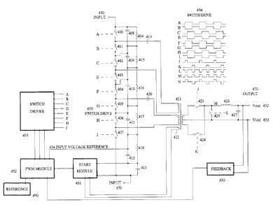
The Embodiment in FIG. 4, in accordance with the present invention represents
the full capability of
the HIGH VOLTAGE TO LOW VOLTAGE BI-DIRECTIONAL CONVERTER. Typically HIGH
VOLTAGE in this embodiment refers to voltages greater than 800 Volt and LOW
VOLTAGE to less than
200 Volt, though the CONVERTER may be designed to operate at any INPUT and
OUTPUT voltage. With
proper PWM MODULE 432 signals The CONVERTER in this embodiment, when designed
with AC or BI-
DIRECTIONAL SWITCHES in all SWITCH locations, 400 through 407, 423, 424, 425
is capable of the
following
CA 02513599 2005-08-09
1. Converting a HIGH VOLTAGE DC or AC INPUT into a regulated LOWER VOLTAGE DC
or AC
output.
2. Converting a LOWER VOLTAGE DC or AC INPUT into a regulated HIGH VOLTAGE DC
or AC
output.
3. Converting a HIGH VOLTAGE DC INPUT into a regulated LOW VOLTAGE AC OUTPUT
of a
frequency equal too or typically much lower than the switch frequency.
4. Converting a LOW VOLTAGE DC INPUT into a regulated HIGH VOLTAGE AC OUTPUT
of a
frequency equal too or typically much lower than the switch frequency.
5. Converting a HIGH VOLTAGE AC INPUT of a frequency equal too or typically
much lower than
the SWITCH frequency into a regulated LOW VOLTAGE DC OUTPUT.
6. Converting a LOW VOLTAGE AC INPUT of a frequency equal too or typically
much lower than
the SWITCH frequency into a regulated HIGH VOLTAGE DC OUTPUT.
FIG. 4 is similar in design to FIG. 3 except that the output section has been
changed by replacing
each DIODE in the secondary circuit with a SWITCH. The converter is intended
to produce a regulated DC
or AC output but may be modified to produce an unregulated DC or AC output by
omitting FEEDBACK
430.
An explanation of the function of the various parts of the embodiment is as
follows. The HIGH
VOLTAGE is connected to INPUT 450 and 451. SWITCHES 401 through 407 are bi-
directional or AC type
and allow the operation from a DC or AC HIGH VOLTAGE power source. SWITCHES
401 through 407
may be DC type if the HIGH VOLTAGE is always going to be DC and will allow
full bi-directional
operation if the DC switches have a reverse diode across them to bypass
reverse current around the switch.
SWITCHES 423, 424, 426 are typically bi-directional and may be replaced with
diodes if the circuit
operation similar to FIG. 3 is required.
SWITCH 400, 401 form one half bridge and 402, 403 form the other side of a
half bridge which is
combined and operated as a full bridge with CAPACITOR 419 blocking the DC
component from being
applied to the primary of transformer 421. Both half bridges operate at full
duty, with each switch ON for
50% of the time. To create a PWM output the phase of the half bridge 402, 403
is shifted from that of
switches 400, 401 by an amount equal to the desired pulse width. SWITCH DRIVE
454 provides an example
of this, with signal A the position of the SWITCH 400, HIGH or UP representing
the ON or CLOSED state,
B, C, D corresponds to SWITCH 401, 402, 403 accordingly and N represents the
difference signal that
appears across the primary of TRANSFORMER 421. The duty of the primary
wavefonn N on
TRANSFORMER 421 can be changed by varying the phase of SWITCH signals A, B
with respect to C, D.
This type of switching method facilitates the use of isolation transformers
for coupling the gate signals to the
SWITCHES and can accommodate any PWM duty from 0 to 100% without worry of
saturation of the
SWITCH driver transformers, not shown in the drawing. SWITCHES 404, 405 form
one half bridge and 406,
407 form the other half bridge of a full-bridge and function in combination
with CAPACITOR 420 and
another primary of TRANSFORMER 421 in the same manner as SWITCH 400, 401, 402,
403, CAPACITOR
419. The same primary of TRANSFORMER 421 may be used for each full bridge if
at least one additional
CAPACITOR is used in series with the junction of SWITCH 402 and 403 or
405,407.
An example of the switch drive waveforms is shown by SWITCH DRIVE 454 which
demonstrates
operation at a duty cycle of 33%. In this example a single TRANSFORMER 421 is
used but the use of
separate TRANSFORMERS as in FIG. 3 will not change the basic function of the
converter, with the
secondary combined or operated with their own output SWITCH. In FIG. 4 SWITCH
423, 424 replace the
DIODES 325, 326 in FIG. 3. In FIG. 4 SWITCH 425 is new and is required for
different operating modes but
can improve the efficiency in all designs. SWITCH 425 is closed or ON when
ever SWITCH 423 or 424 are
both OFF or open, thus providing a return path for INDUCTOR 426 current to
CAPACITOR 427. Failure to
provide a return path for INDUCTOR 426 current would cause the build up of a
very high voltage across
CA 02513599 2005-08-09
SWITCH 423 and 424 when they are first OPENED. SWITCH 425 may be omitted in
designs that use PWM
control on the primary of TRANSFORMER 421 so long as the drive for SWITCH 423
and 424 is modified
such that they are both ON as indicated in SWITCH DRIVE 454 as well as both
are turned ON or remain ON
when ever the SWITCH 425 was indicated as being ON. When SWITCH 425 is left
out or replaced by a
DIODE then SWITCH 423, 424 may be operated as synchronous rectifiers and
derive their switch signals
directly from extra windings on TRANSFORMER 421, not shown in FIG. 4, as that
method is already in use
by PRIOR ART. The inclusion of SWITCH 425 allows for a special operating mode
where the primary of
TRANSFORMER 421 is a full duty square wave, not PWM modulated, but instead
SWITCH 423, 424 are
operated in a PWM mode. The output circuit of FIG. 4 comprising of SWITCH 423,
424, 425, Inductor 426
and CAPACITOR 427 may be applied and used in a similar manner to PRIOR ART
shown in FIG. l and FIG.
2, providing bi-direction operation that currently doesn't exist in those
embodiments.
SWITCH 423, 424 rectify the output of TRANSFORMER 421 and apply the pulsating
rectified DC
pulses shown by waveform M on the SWITCH DRIVE table 454 to an INDUCTOR 426
and CAPACITOR
427, which are then filtered to the desired degree. IF a second output circuit
and TRANSFORMER is used
similar to FIG. 3 and the second TRANSFORMER is operated phase shifted by 90
degrees then the ripple
frequency across CAPACITOR 427 will be doubled and the pulsating DC currents
greatly reduced allowing a
much smaller capacitor value to be used. This technique may be extended
further using a plurality of
TRANSFORMERS and plurality of secondary combined in this manner.
CAPACITORS 408, 409, 410, 411, 412 filter the switch current pulses reducing
the high frequency
AC that is generated by the half bridges in series across the INPUT 450 and
451. The addition of
RESISTORS 414, 415, 416, 417 and 418 are used to force the voltages to be
equal across CAPACITORS
408, 409, 410, 411, 412 during the start-up time that the half bridges are
off. CAPACITOR 413 is used to
provide start-up power for the START MODULE 431, which has various internal
components that store
sufficient charge to run the SWITCHES for a specific time after which an
auxiliary winding 422 from
TRANSFORMER 421 supplies the necessary power to run the control electronics.
Alternately, an external
DC or AC power source, not shown, provides the power to operate the DC to DC
converter and may be
common to or close to either INPUT 450 or 451.
In FIG. 4 INPUT VOLTAGE REFERENCE 434 provides input polarity, REFERENCE 490
provides
a voltage proportional to the desired output voltage and FEEDBACK 430 supplies
a feedback signal
proportional to the secondary output voltage all of which are used by the PWM
MODULE 432 to generate
the appropriate PWM phase clock signals that are supplied to the SWITCH DRIVER
433, which then drives
the switches 400, 401,402, 403, 404, 405, 406, 407, 423, 424, 425. These
circuits function as follows. When
HIGH VOLTAGE is first applied to INPUT 450 and 451, the RESISTORS 414, 415,
416, 417 and 418
charge CAPACITOR 413. The START MODULE 431 takes the charge from CAPACITOR 413
and
determines when it has enough charge to operate the PWM MODULE 432 and SWITCH
DRIVER 433 for a
predetermined time. For operation from a HIGH VOLTAGE AC INPUT the START
MODULE 431 takes
the current normally charging CAPACITOR 413 and rectifies it and stores the
charge internally until a
sufficient level has built up to initiate startup of the power supply.
Alternately, the START MODULE 431
may be powered by an external low voltage DC or AC source, not shown in FIG.
4. After initially powering
the converter electronics, the START MODULE 431 receives a low voltage AC from
TRANSFORMER 421
through SECONDARY 422. The power from this SECONDARY 422 then provides the low
voltage power to
sustain operation of the PWM MODULE 432 and SWITCH DRIVER 433.
Further in FIG. 4, after the START MODULE 431 has started the converter the
FEEDBACK 430
provides to the PWM MODULE 432, a signal, that is proportional to the output
voltage. The FEEDBACK
430 may use optical isolation, an isolation transformer etc., none of which
are shown, to provide this isolated
feedback signal to the PWM MODULE 432. However, the typical design requires
higher isolation voltage
between the primary and secondary of TRANSFORMER 421 and across the FEEDBACK
430 than that
CA 02513599 2005-08-09
required by conventional commercial power supply designs. PWM MODULE 432
generates two or more
square-wave outputs that have the phase of their outputs shifted proportional
to the duty of the waveform that
is to be applied to the primary of TRANSFORMER 421. SWITCH DRIVE 433 provides
the necessary
isolation of the drive signals with the correct phase to switches 400, 401,
402, 403, 404, 405, 406, 407, 423,
424 and 425. Typical waveforms are shown in SWITCH DRIVE 454, representing an
operating duty of
33%.. SWITCH 423, 424 rectify the pulsating AC waveform looking as signal N of
the SWITCH DRIVE
454 of the of the secondary of TRANSFORMER 421 into a pulsating DC, shown as
M, which is then filtered
by INDUCTOR 426 and CAPACITOR 427. The output INDUCTOR 426 and CAPACITOR 427
filters the
pulsating signal M into a average value equal to the duty of the waveform
times it's peak amplitude. The
circuit functions in a similar manner as a switching power supply commonly
called a FORWARD
CONVERTER. In FIG.4 when HIGH VOLTAGE AC is applied to INPUT 450 and 451,
acceptable as all
switches are bi-directional, then the low voltage output VOUT 452 and 453 will
be regulated AC and reduced
in amplitude. A expression for the output voltage when the input AC or DC is
being converter to a regulated
lower voltage of the same type of waveform is
Vp = Vin / Bn
2 Vout = Vp * D / N
Where:
Vp => TRANSFORMER PRIMARY VOLTAGE
Vin => HIGH VOLTAGE INPUT
Bn => NUMBER HALF-BRIDGES
Vout => OUTPUT VOLTAGE
N => TRANSFORMER TURNS RATIO ; Number Primary turns divided by Number
Secondary turns
D => DUTY
DUTY is the ratio of the time the Primary is ON divided by the sum of Primary
OFF plus ON time.
Equation 2 is important as it establishes the ratio between the input and
output voltage. The power supply
is fully bi-directional such that should the power supply output rise to a
value greater than equation 2 allows,
power will flow from the output back to the input. This has numerous
advantages, for example accelerating a
car from a high voltage battery, then by changing the power supply duty the
power supply acts as a
regenerative brake returning the energy from stopping the car to recharge the
high voltage battery.
In FIG. 4 the INPUT VOLTAGE REFERENCE 434 is used by the PWM MODULE 432 when
it is
necessary to convert from AC to DC or vice versa. The signal is used to
determine whether the phase of the
SWITCH 423 and 424 has to be inverted from its normal condition, thus changing
equation 2 to
3 Vout=P*Vp*D / N
Where
P => POLARITY is either +1 or - 1 depending on whether the phase of SWITCH 423
and 424 is
inverted to the normal stated, providing a reversed OUTPUT voltage with
respect to the INPUT.
CA 02513599 2005-08-09
The effect of the phase is to change VOUT 452, 453 polarity with respect to
the INPUT 450, 451. For
example using a PHASE of -1 changes a positive HIGH VOLTAGE DC INPUT to a
negative LOWER
VOLTAGE DC OUTPUT. Alternately, a PHASE of -1 a positive HIGH VOLTAGE AC INPUT
would
change to a negative or reversed phase LOWER VOLTAGE AC OUTPUT.
INPUT VOLTAGE REFERENCE 434 has other uses as well, especially when converting
a HIGH
VOLTAGE AC INPUT to a LOWER VOLTAGE DC OUTPUT or vice versa. For example when
converting a HIGH VOLTAGE AC INPUT in to a positive LOWER VOLTAGE DC OUTPUT
then the
POLARITY signal +1 when the HIGH VOLTAGE AC INPUT is positive and -1 when the
HIGH
VOLTAGE AC INPUT is negative. The resultant DC OUTPUT will be the same as any
full wave
rectified AC signal, the amplitude and ripple characteristics will be
determined by the value of the filter
made up of INDUCTOR 426 and CAPACITOR 427 however, the voltage at point M will
be determined
by equation 3.
To convert a HIGH VOLTAGE DC INPUT to a LOW VOLTAGE AC OUTPUT then the
POLARITY control is used to toggle or change to the opposite state the LOW
VOLTAGE OUTPUT
every time the AC REFERENCE 490 waveform goes through a zero crossing. To
synthesize an AC
waveform it is necessary for the PWM MODULE 432 to use a modified REFERENCE
490 as it requires
a value which is proportional to the desired output waveform. Typically a look
up table in a micro-
processor memory or logic storage device is used to synthesize a suitable
REFERENCE 490 signal. The
FEEDBACK 430 value is compared to the REFERENCE 490 waveform and the PWM is
adjusted as
required to produce the correct output. The technique is well known in the
Industry and is may be found
in a number of the Patents listed as PRIOR ART. Conversely, a LOW VOLTAGE DC
OUTPUT may
be converted to a HIGH VOLTAGE AC OUTPUT if the magnitude of the DC OUTPUT
present on
VOUT 452, 453 is greater than that allowed by equation 3. The power under this
circumstance will then
flow from the LOW VOLTAGE VOUT side to the HIGH VOLTAGE INPUT.
FIG. 7 shows that the SWITCH 423, 424 in FIG. 4 can be substituted with a full
wave bridge, using 4
SWITCHES instead of the two in FIG. 4. This is the case when the use of a
center tapped secondary such
as that used by TRANSFORMER 421 in FIG. 4 is not desired. The arrangement in
FIG. 7 shows a typical
full bridge secondary circuit where SWITCH 722, 723 are the same phase as
SWITCH 423 in FIG. 4 and
SWITCH 721, 724 are the same phase as SWITCH 424 in FIG. 4. Other similarities
between FIG. 7 and
Fig. 4 are TRANSFORMER 720 & 421; SWITCH 725 & 425; INDUCTOR 726 & 426;
CAPACITOR
727 & 427; FEEDBACK 730 & 430 etc. are all the same as well as remaining
components except instead
of a leading 4 there is leading 7 substituted in FIG. 7. The function of the
circuit with the changed
secondary circuit is exactly the same as in FIG. 4 except for the substitution
of the appropriate number
from FIG. 7 into the description for FIG. 4.
FIG. SB shows the definition of what is meant by a DC switch. The DC switch
behaves as a switch
blocking voltage in one direction but when a reverse voltage is applied it
either conducts as in the case of
DIODE 505 or is destroyed. That is why typically a DIODE 505 is placed across
the SWITCH 504 as
shown in FIG. SB. The FIG. SC shows a BI-DIRECTIONAL SWITCH 508 made up using
two mosfets
506 and 507. Each mosfet is in this example have their SOURCE terminals
connected together and the
control signal is applied across the G and S terminals. The terminals labeled
A on device 506 and B on
device 507 are the equivalent SWITCH input and output terminals. The Mosfets
506 and 507 may be
connected Drain to Drain instead of the way shown, however in that method each
will require a separate
isolated G and S drive signal. Any type of switch semiconductor or otherwise
may be substituted for
Mosfet 506 and 507 so long as they are combined in a way that the switch will
block voltage of any
polarity when turned off and pass current of any polarity when turned on. It
should be pointed out that
most switch designs that use semi-conductor devices use additional components
not shown in any FIG. 1
through 7. These additional devices are used following manufacturer's
recommendation or through good
CA 02513599 2005-08-09
11
design practice for the purpose of protecting the switch from overload
current, reverse voltage, voltage,
power, temperature and for reducing electronic radiated noise. Mounting and
cooling of the switches is
selected to suit a designs mechanical and performance requirements and the
preferred embodiments do
not have any special design requirements other than that required to meet a
specific product reliability.
FIG. 6A shows a typical filter block that may be added to the LOW VOLTAGE
OUTPUT side to
improve the quality of the output. FIG. 6B shows a typical filter block that
may be added to the HIGH
VOLTAGE INPUT side to reduce the radiated noise caused by the INPUT SWITCH
action. These filters
typically are composed of a combination of INDUCTORS, CAPACITORS and RESITORS
in differing
combinations to generate the required noise attenuation ratio required by the
design. The preferred
embodiments does not impose or require any special filter design other than
that used by good practice.
The embodiments of FIG. 3 and FIG. 4 may be operated using PWM control or
alternately using a
variable frequency switching rate with a fixed or variable ON pulse width.
FIG. 8 Is a preferred embodiment that uses the converter for powering an
electric motor, such as in
hybrid electric car etc.. The POWER SOURCE 800 such as a battery or capacitor
bank, fuel cell, or any
combination of these or an AC source such as the output from a motor-generator
connected to a fly-wheel,
provides a source of power to operate the DRIVE MOTOR 813. The DRIVE MOTOR 813
may be DC or a
poly-phase AC motor using one or plurality of AC phases provided by a
plurality N of converters as shown
by SUPPLY A 810, SUPPLY B 811, through SUPPLY N 812. These power supplies may
be wholly
independent or share various common elements from each other, such as feedback
or PWM CONTROL
signals and they may even have a common primary section but multiple
secondary, each providing a different
output phase. In FIG. 8 DC POWER SOURCE 800, it is connected the HIGH VOLTAGE
side of the
converter and the low voltage side connected to the DRIVE MOTOR 813. The DRIVE
MOTOR 813 may be
replaced by any other electric device. In keeping with the preferred
embodiment of the converter it can use an
AC source of a differing frequency, such as that put out by the motor-
generator of a fly-wheel to create a
different frequency AC output to the DRIVE MOTOR 813. During acceleration or
steady operation of the
DRIVE MOTOR 813 the converters SUPPLY A 810, SUPPLY B 811, SUPPLY N 812 takes
its power from
the POWER SOURCE 800, energy may be transferred from the DRIVE MOTOR 813 back
to the POWER
SOURCE 800 using regenerative-breaking, where DRIVE MOTOR 813 is changed to a
generator and used
to decelerate the rate that it is turning. The operation in this mode exploits
the use of equation 2 or 3 from
earlier in this section along with specific clocking signals that are unique
to each application. The best
example of this would be where the DRIVE MOTOR 813 is used in an automobile as
either the whole or
partial motive source though, the preferred embodiment is not limited to this
application.
FIG. 9 is similar to FIG. 8 but the POWER SOURCE 904 is now located on the LOW
VOLTAGE
side and the DRIVE MOTOR 903 is on the HIGH VOLTAGE side. The operation in
this mode is identical
just the direction of power flow is different under the same circumstance.
Another preferred embodiment, no figure provided can be a HIGH VOLTAGE to HIGH
VOLTAGE
converter where instead of a LOW VOLTAGE secondary circuit, the secondary uses
a HIGH VOLTAGE
arrangement of half bridges in series similar to the primary side.
Another preferred embodiment again no figure provided, would use the HIGH
VOLTAGE switch
arrangement of FIG. 1 or FIG. 2 on the primary and the secondary arrangement
of FIG. 4 or FIG. 7. A
variation of this would be where the secondary switch arrangement of FIG. 4 or
FIG. 7 would be PWM
operated and the primary side would be a 100% duty square-wave and the
variable DUTY of the secondary
switches would provide the PWM regulation. This arrangement is shown in FIG.
10 the SWITCH DRIVE
1054A, where SWITCH signals A through G are the same as those from SWITCH
DRIVE 154 of FIG. I .
SWITCH DRIVE signals J, K, L, M, N are the same signals as that from SWITCH
DRIVE 454 of FIG. 4 and
CA 02513599 2005-08-09
12
would be the switching signals of the secondary SWITCH 423 as J, SWITCH 424 as
K and SWITCH 425 as
L where M is the rectified output the same as FIG. 4 and N is the secondary or
primary waveform. The
operation is similar to FIG. 4 or FIG. 7 except that the secondary side is the
only switches that have their
signals PWM. Another arrangement is possible as shown by FIG. 10 SWITCH DRIVE
1054B again the same
circumstance but where the primary is PWM as well as the secondary. The
signals from SWITCH DRIVE
1054B relates to A through G as the switch signals of FIG. 2 SWITCH 200
through 205 respectively and
FIG. 4 or 7 is the secondary SWITCH 423 as J, SWITCH 424 as K and SWITCH 425
as L where M is the
rectified output the same as FIG. 4 and N is the secondary or primary
waveform. FIG. 10 is bi-directional of
any polarity input or output if the secondary switches are bi-directional and
the primary side switches of FIG.
1 or FIG. 2 are made bi-direction.
Although the invention has been described in connection with a preferred
embodiment, it should be
understood that various modifications, additions and alterations may be made
to the invention by one skilled
in the art without departing from the spirit and scope of the invention as
defined in the appended claims.