Note: Descriptions are shown in the official language in which they were submitted.
CA 02513984 2005-07-28
Field of the Invention
The invention is generally directed to the control of a light source
responsive to ambient light.
Background of the Invention
Photosensitive controls are utilized in a number of environments where
it is desirable to turn a light source on or off depending upon the amount of
ambient light. For example, in landscape lighting applications, it may be
desirable to automatically turn lights on at dusk and turn lights off at dawn,
or
alternatively, after a fixed number of hours after dusk. In addition, it may
be
desirable in some motion sensing or security applications to sense the
amount of ambient light to prevent a motion-sensitive light from turning on
during the day. One challenge that is encountered with respect to
photosensitive controls, however, results from the feedback of light from a
controlled light source to the light detector used in determining the ambient
light level. In some photosensitive controls, for example, a light detector
output is compared to a static threshold that the light source is turned on
when the ambient light falls below that threshold, and turned off when the
ambient light rises above that threshold. However, when a light source is
turned on, a portion of the generated light may be detected by the light
detector, and may cause the detector input to rise above the static threshold,
and cause the photosensitive control to turn the light back off. In some
instances, the light source may flicker or repeatedly cycle on and off as a
result of the feedback of light from an activated light source.
1
CA 02513984 2005-07-28
Some attempts to minimize the effect of feedback have included
shielding a light detector or otherwise placing the light detector in a
location
that minimizes the amount of light from the controlled light source that Is
fed
back to the detector. However, depending upon where the light source and
light detector are installed, surrounding structures such as walls and other
reflective surfaces may nonetheless reflect light from the light source back
to
a light detector. As a result, the amount of light feed back to a light
detector
may vary from installation to installation, and is thus difficult to eliminate
through shielding or placement of the light detector.
Additional attempts to minimize the effects of feedback include using
hysteresis to set different on and off thresholds, thus requiring a greater
amount of ambient light to be detected to turn a light source off than that
used
to turn the light source on. It has been found, however, that increasing the
"window" between on and off thresholds can inhibit accurate dawn detection,
particularly on overcast days.
Other attempts to minimize the effects of feedback include dynamically
setting thresholds based on the amount of ambient light sensed by a light
detector. One conventional. implementation, for example, monitors the
infrared output of a fluorescent light and sets an off threshold based upon
the
amount of infrared light sensed after the fluorescent light is turned on,
typically
after waiting until the rate of change of the infrared output has decreased
and
the output has stabilized. Also, in this implementation, a rate of change of
the
light detector output may be used along with the absolute output to minimize
the effects of rapid changes in the light detector output.
2
CA 02513984 2005-07-28
One problem associated with the aforementioned implementation,
however, Is that sensing the rate of change of a light detector output
typically
requires relatively complex processing. Moreover, sensing the rate of change
may limit the overall responsiveness of the light detection circuit.
Therefore, what is needed is a simple and responsive photosensitive
control that reduces the adverse effects of feedback from a controlled light
source.
Summary of the Invention
The invention addresses these and other problems associated with the
prior art by providing a method and circuit arrangement that dynamically
calibrates a photosensitive control for a light source. In particular, a
photosensitive control consistent with the Invention includes a voltage
divider
circuit coupled to a resistive light detector and configured to output to a
comparison circuit a variable voltage signal that varies with the resistance
of
the resistive light detector. To calibrate the photosensitive control, a
variable
impedance circuit in the voltage divider circuit including, for example, a
variable resistor, is adjusted to bias the variable voltage signal.
These and other advantages and features, which characterize the
invention, are set forth In the claims annexed hereto and forming a further
part
hereof. However, for a better understanding of the invention, and of the
advantages and objectives attained through its use, reference should be
made to the Drawings, and to the accompanying descriptive matter, in which
there is described exemplary embodiments of the invention.
3
CA 02513984 2005-07-28
Brief Description of the Drawings
FIGURE 1 is a block diagram of a photosensitive control for a light
source consistent with the invention.
FIGURE 2 Is a flowchart illustrating exemplary steps utilized in a reset
routine executed by the photosensitive control of Figure 1.
FIGURE 3 is a flowchart of the self-calibrate routine referenced in
Figure 2.
FIGURE 4 is a block diagram of an exemplary implementation of a
calibration circuit utilized in the photosensitive control of Figure 1.
FIGURE 5 is a flowchart illustrating exemplary steps utilized in a reset
routine executed by the photosensitive control of Figure 1.
Detailed Description
Turning to the drawings, wherein like numbers denote like parts
throughout the several views, Figure 1 illustrates a photosensitive control 10
consistent with the invention. Photosensitive control 10 is used to control a
light source 12, which may include, for example, one or more incandescent or
fluorescent light sources, among other sources of the light. In the
alternative,
control 10 may be used to power a wireless transmitter such as an RF
transmitter for activating a remote light source In response to a logical
activation signal. Control 10 includes a light controller or processor 14 to
which is coupled a light detector 16. Light controller 14 may be Implemented,
for example, as an integrated circuit chip, while light detector 16 may be
implemented using any known photosensitive detector or sensor, e.g., a
photoconductive sensor such as a cadmium sulfide (CdS) detector,
photodiode, phototransistor, etc.
4
CA 02513984 2005-07-28
In the illustrative embodiment, light detector 16 is implemented as a
resistive light detector, wherein the resistance or impedance of the detector
varies with the amount of light Incident on the detector. Other light detector
implementations may be used in the alternative.
AC power to photosensitive control 10 is provided via lines 18, 20, with
a power supply 22 used to regulated and convert the AC power to DC power
for use by controller 14. The device may also be DC, battery, solar powered,
etc. in which case a simpler power supply may be used, or the power supply
may be eliminated completely if unnecessary. A power control block 24, e.g.,
a relay or other switching device, is coupled between lines 18, 20 in series
with light source 12, and is controlled by light controller 14 to selectively
power light source 12.
In the illustrative embodiment, photosensitive control 10 additionally
has motion sensing capability, whereby one or more motion sensors 26, e.g.,
passive infrared (PIR) sensors, are coupled to a network of cascaded
amplifiers, e.g., including an external amplifier circuit 28 and additional
integrated amplifiers 30 in light controller 14.
it may also be desirable in some implementations to provide a line
conditioning circuit 32 for the purpose of providing light controller 14 with
a
time base from the AC power lines 18, 20. The time base may be used for
timing on and off times, as well as for sensing power fluctuations or
failures,
e.g., due to electrical storms or other power outages, and thereby modify the
operation of the photosensitive control based upon such detected fluctuations.
Photosensitive control 10 may be used In a wide variety of applications,
and may utilize a number of known functions in the control of a light source
5
CA 02513984 2005-07-28
consistent with the invention. For example, light controller 14 may be
configured to activate a light source responsive to motion detected via one of
sensors 26, and thereafter deactivate the light after expiration of a fixed
timer.
Furthermore, activation of the light source may further be conditioned upon
the level of ambient light so that the light source will not be turned on in
response to detected motion during the daytime. It may also be desirable to
provide a manual override function whereby the light source may be activated
irrespective of whether motion is sensed.
It will be appreciated that the invention may be utilized in a wide variety
of other photosensitive control applications consistent with the invention.
For
example, the invention may be utilized in any application where it Is
desirable
to control the activation of a light source based upon ambient light level,
including non-motion sensing applications.
Now turning to Figure 2, an exemplary reset routine 50, executed by
light controller 14 upon initial reset and power up of light controller 14, is
illustrated in greater detail. Routine 50 begins in block 52 by initially
setting
the controller to a "day" or off state and deactivating the light source.
Control
then passes to block 54 to set a state transition threshold to a night detect
threshold, i.e., a level of detected ambient light below which the
photosensitive control will transition from a day (off) to night (on) state.
In the
illustrative embodiment, it is assumed that with the light source deactivated
in
such a state, the amount of extraneous ambient light that is not reflective of
the time of day will be negligible, so a default, static threshold .is
selected for
the night detect threshold. In other implementations, however, it may be
desirable to dynamically generate the night detect threshold Instead.
6
CA 02513984 2005-07-28
Next, control passes to block 56 to monitor the ambient light level with
the light detector, and then to block 58 to determine whether the night detect
threshold has been met. If the threshold is not met, light controller 14
continues to monitor the ambient light level by returning control to block 56.
Otherwise, if the night detect threshold has been met (e.g., where the
ambient light level falls below the night detect threshold), control passes to
block 60 to set the controller in a night (on) state and active the light
source.
Control then passes to block 62 to perform a self-calibrate routine, which
dynamically sets a day detect threshold that is used in determining when to
switch back to the day (off) state.
Figure 3, for example, illustrates one suitable implementation of self-
calibrate routine 62. In particular, route 62 begins in block 64 by initiating
a
delay for a predetermined amount of time to allow the light source to reach a
relatively steady state, e.g., about 3 to 5 seconds. Next, block 66 detects
the
ambient light level with the light detector, and thereafter block 68
dynamically
generates the day detect threshold based upon the detected ambient light
level.
Returning to Figure 2, once the day detect threshold has been
dynamically generated, control passes to block 70 to monitor the ambient light
level with the light detector. Based upon whether the day detect threshold is
met, block 72 either returns control to block 70 (if the threshold is not met)
or
passes control to block 52 (if the threshold is met), the latter condition
returning the controller to the day (off) state and deactivating the light
source.
It will be appreciated that routine 50 may directly active a light source,
or in the alternative, may simply enable activation of the light source, where
7
CA 02513984 2005-07-28
the actual activation of the light source is further conditioned on additional
criteria. For example, in a motion sensing implementation, it may be desirable
for routine 50 to simply enable and disable activation of a light source
during
the night and day states, respectively, so that the light source will be
turned
on in response to motion detected by a motion sensor only when the
controller is in the night state.
It will also be appreciated that, while self-calibrate routine 62 Is shown
being executed to dynamically generate a threshold only after the controller
transitions from an 'off" state to a "on" state, routine 62 may also be
executed
to generate a threshold in a number of different circumstances. For example,
routine 62 may be executed when switching a light source between different
luminance levels, e.g., when switching between bright and dim modes. Also,
as noted above, routine 62 may be executed upon switching from an "on"
state to an "off" state, e.g., as opposed to setting a static threshold as is
done
in block 54 of routine 50. Other modifications will be apparent to one of
ordinary skill in the art having the benefit of the instant disclosure.
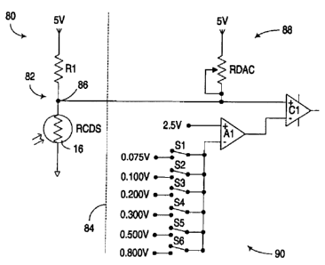
Figure 4 next illustrates one specific implementation of a calibration
circuit 80 consistent with the invention. Figure 4, In particular, illustrates
an
exemplary implementation partially integrated into light controller chip 14,
with
the components to the right of dashed line 84 being integrated into light
controller chip 14, and the components to the left of line 84 being disposed
external to the chip. Calibration circuit 80 Includes a voltage divider
circuit 82
coupled to one input of a comparison circuit, e.g., coupled to the positive
(+)
input of a comparator C1.
8
CA 02513984 2005-07-28
Voltage divider circuit 82 is coupled between power (VDD) and ground,
and includes a common node 86 coupled to the positive input of comparator
C1. Coupled between VDD and common node 86 is a variable impedance
circuit 88 comprising a parallel arrangement of a fixed resistor Rt and a
variable resistor RDAC. Light detector 16, implemented as a resistive CdS
detector (denoted in Figure 4 as RCDS), Is coupled between common node
86 and ground. As will be discussed in greater detail below, resistors R1 and
RDAC provide a variable impedance capable of biasing a variable voltage
signal that varies with the level of ambient light sensed by light detector 16
and that is output to the positive input of comparator C1.
Coupled to the negative (-) input of comparator C1 is a reference signal
generation circuit 90 comprising an adder Al and a series of switches S1-S6.
Adder Al has a positive (+) input coupled to a fixed reference voltage, e.g.,
VDD/2 volts, or 2.5 volts where VDD=5 volts, for example. The negative (-)
input to adder Al is coupled to a plurality of discrete offset voltages via
switches S1-S6. Each switch is a digitally-controlled switch which, when
closed, passes one of a plurality of offset voltages to adder Al and thus
decrease the reference voltage output thereby. In the illustrative embodiment,
for example, six discrete offset voltages may be selected via switches Si-S6,
including 0.075 volts, 0.100 volts, 0.200 volts, 0.300 volts, 0.500 volts, and
0.800 volts. It will be appreciated that other offset voltage generating
circuits,
e.g., that generate non-discrete offset voltages, may be used in the
alternative.
Also in the illustrative implementation, variable resistor RDAC is
implemented as a digitally-controlled resistor, e.g., a resistive digital to
analog
9
CA 02513984 2005-07-28
converter (RDAC) including a R-2R ladder arrangement, as is well known in
the art. In the illustrative embodiment, for example, the RDAC may be
implemented as a 10-bit converter having a maximum resistance of about 250
KOhm. The Impedance of the R-2R ladder may be controlled, for example, by
a digital counter. The impedance of the RDAC would then be directly
proportional to the count value chosen by this counter. It may also be
desirable to implement resistor R1 with a resistance of about 39 KOhm, such
that the effective resistance of the parallel configuration of resistors R1
and
RDAC has a maximum resistance of about 33.7 KOhm. It will be appreciated,
however, that other circuitry capable of providing a variable impedance to
bias
the variable voltage signal generated by light detector 16, e.g., using
various
combinations of other resistors, capacitors, inductors, current sources,
active
components, etc., may be used as an alternative to the parallel arrangement
of resistors R1 and RDAC.
During normal daytime operation, the impedance of RDAC would be
set to maximum and switches S1 through S6 would be open. As the ambient
light levels decrease, the impedance of RCDS will Increase and eventually the
voltage at node 86 will rise above the reference voltage Voo12i or for
example,
2.5V and the output of comparator C1 will change states. Assuming that the
external light source is turned on at the time, light feedback will decrease
the
impedance of RCDS and the voltage at node 86 will decrease to an extent
that depends directly upon the amount of light that Is fed back. In general,
calibration circuit 80 operates by first adjusting resistor RDAC to bias the
variable voltage signal at node 86 until the variable voltage is greater than
or
equal to 2.5 volts. This action effectively cancels the error caused by any
light
CA 02513984 2005-07-28
feedback. Thereafter, the reference voltage is generated based upon the
count in the RDAC used to bias the variable voltage signal. The offset Is
selected for different ranges of count values, although alternate formulas or
algorithms may be utilized in the alternative. For example, it may be
desirable
to provide an offset of 0.075 volts for a count value below 21, an offset
voltage
of 0.100 volts for a count between 21 and 30, an offset voltage of 0.200 volts
for a count between 31 and 50, an offset voltage of 0.300 volts for a count
value between 51 and 100, an offset voltage of 0.500 volts for count value
between 101 and 225, and an offset voltage of 0.800 volts for a count value
greater than 226.
As such, calibration circuit 80 generally provides a variable threshold
based upon the sensed ambient light. Of note, this variable threshold may
also be considered to be a variable window between the switch off and switch
on thresholds.
It will be appreciated that the profile of such a variable window may
vary in different implementations of the invention. Generally, it is desirable
in
many implementations to set the comparator offset voltage to be large enough
to provide adequate head room when the feedback luminance is relatively
small, but is desirably is kept as small as possible to minimize errors when
the
feedback luminance is relatively large.
Figure 5 next illustrates an exemplary reset routine 100 that may be
executed by light controller 14 upon initial power up when the calibration
circuit of Figure 4 is utilized in a photosensitive control consistent with
the
invention. It will be appreciated that routine 100 may be Implemented at least
partially in software or via other programmable circuitry.
11
CA 02513984 2005-07-28
Routine 100 begins In block 102 by setting the controller to a day state
and deactivating the light source. Thereafter, a delay is implemented in block
104 to allow the light source to fully shut off. Next, block 106 adjusts the
RDAC resistor to its maximum (default) resistance, and block 108 sets the
comparator reference voltage to 2.5 volts, i.e., with no offset voltage.
Blocks
106 and 108 therefore have the functionality of setting for the light
controller a
default night detect threshold.
Next, block 110 waits until the comparator output goes high, indicating
that the ambient light level has fallen below the detect threshold. Control
then
passes to block 112 to set the controller to night state, and activate the
light
source.
Next, block 114 waits a predetermined time period, .e.g., about 3 to 5
seconds, and block 116 then progressively adjusts the RDAC to bias the
variable voltage input at comparator C1 to the largest value at which the
variable voltage is about 2.5 volts (e.g., the last value before the
comparator
changes state). Block 118 then latches the count value for the RDAC resistor,
and based upon this latched value, block 120 selects the comparator
reference offset value as described above, and activates the appropriate
switch S1-S6.
Block 122 then waits until the comparator output goes low, indicating
that ambient light level has increased above the threshold dynamically
generated in blocks 116-120. Once the comparator output is detected at low,
block 122 then passes control to block 102 to set the light controller to day
state and deactivate the light source, as described above.
12
CA 02513984 2011-12-30
Various additional modifications may be made to the illustrated
embodiments without departing from the scope of the invention. The
invention is therefore defined in the claims hereinafter appended.
13